Electronics Production
Overview This week's focus was on the fabrication of a printed circuit board (PCB) and the soldering of electronic components onto it. The goal was to design, mill, assemble, and test a functional microcontroller-based circuit using tools and techniques commonly applied in rapid prototyping environments.
PCB Design with KiCad
- The circuit board was designed using KiCad, a powerful open-source electronic design automation (EDA) tool.
- KiCad was used to complete both the schematic design and the PCB layout, which are necessary steps before generating files for fabrication.
- The schematic was created by placing and wiring the components logically.
- Once the schematic was complete, the components were transferred to the PCB layout editor.
- The board layout was adjusted, traces were routed manually, and the board outline was defined.
- For this project, the PCB was designed for single-sided milling, meaning only the top copper layer was used.
- You can find the full schematic and PCB design documentation on Week 6.
Electronic Components Used
The following components were selected and included in the PCB design:
- Seeed XIAO RP2040 – the main microcontroller used in the board.
- Resistors × 2 – current-limiting resistors, one for the LED and another for the button input.
- LED – indicator that lights up when the button is pressed.
- Push Button – used for input control to test functionality.
- Pin Headers – for connecting external modules or for programming the microcontroller.
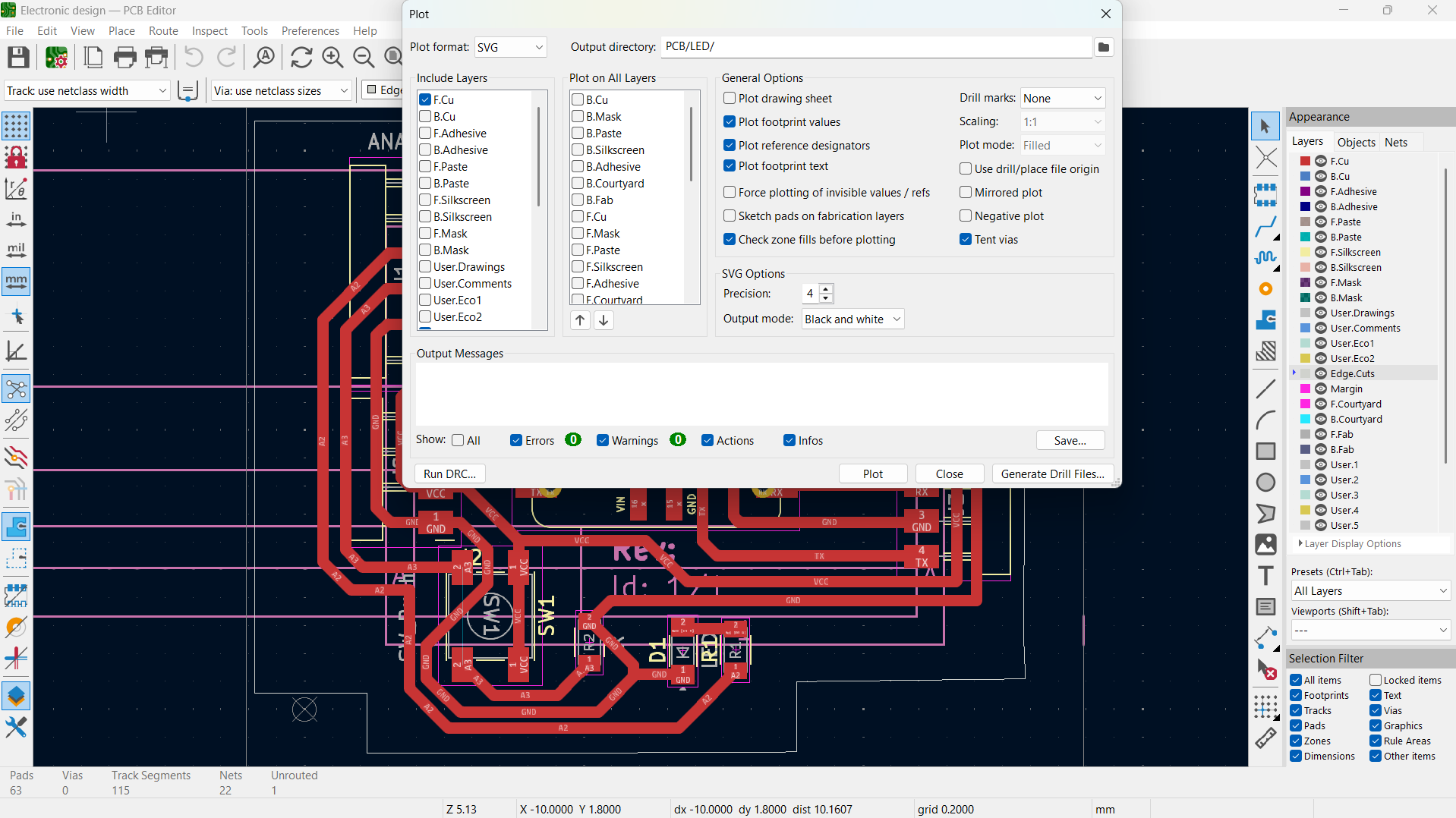
Generating Gerber Files in KiCad
After completing the PCB layout, the next step was to generate the Gerber files required for fabrication. These files define the copper traces and board outline for the milling machine.
Steps to Generate Gerber Files:
- Open the PCB layout in KiCad’s PCB Editor.
- Go to the menu and click on File → Plot.
- Select Gerber as the output format.
- Select the necessary layers for a single-sided board:
- F.Cu – Front copper layer (traces).
- Edge.Cuts – Board outline (used to cut the PCB to shape).
- Click Plot to generate the files.
These Gerber files are typically used for manufacturing PCBs in professional settings, but for this project, they were converted to SVG format for CNC milling.
Generating G-code Files with MODS
To mill the PCB on a desktop CNC machine, the Gerber files were converted into SVG files using the online tool MODS.
Steps to Create G-code Files from Gerber:
- Navigate to the MODS platform and right click on the icon top left to select program.
- Select open programs.
- To import the generated Gerber file or G-code.
- Select the "mill 2D PCB" module under the G-code section.
- Import the SVG version of the Gerber file.
- In the next module, choose Invert to correctly display traces (black lines will be milled out).
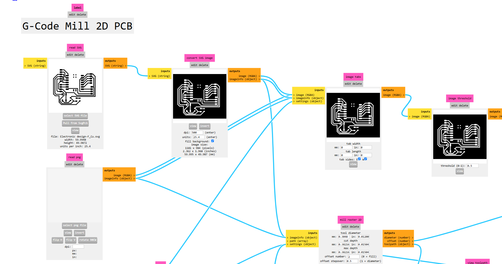
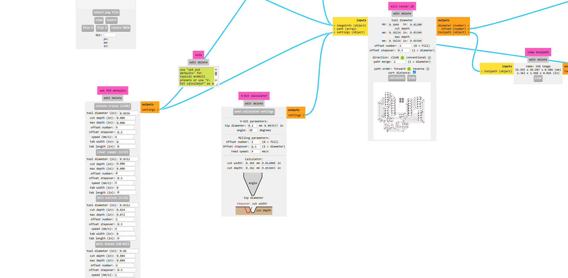
Set Tool Parameters:
- Under Set PCB Defaults, select Mill Trace if only traces are to be milled (not the full board cutout).
- In the V-bit Calculator, enter the correct dimensions of the V-bit tool.
- Click "Send Calculate Settings" to process tool paths.
- Under Mill Raster, click "Calculate" to preview the toolpath and generate the final SVG file.
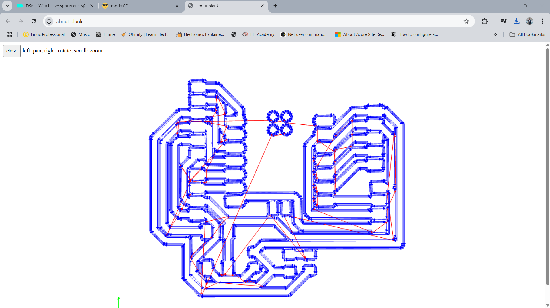
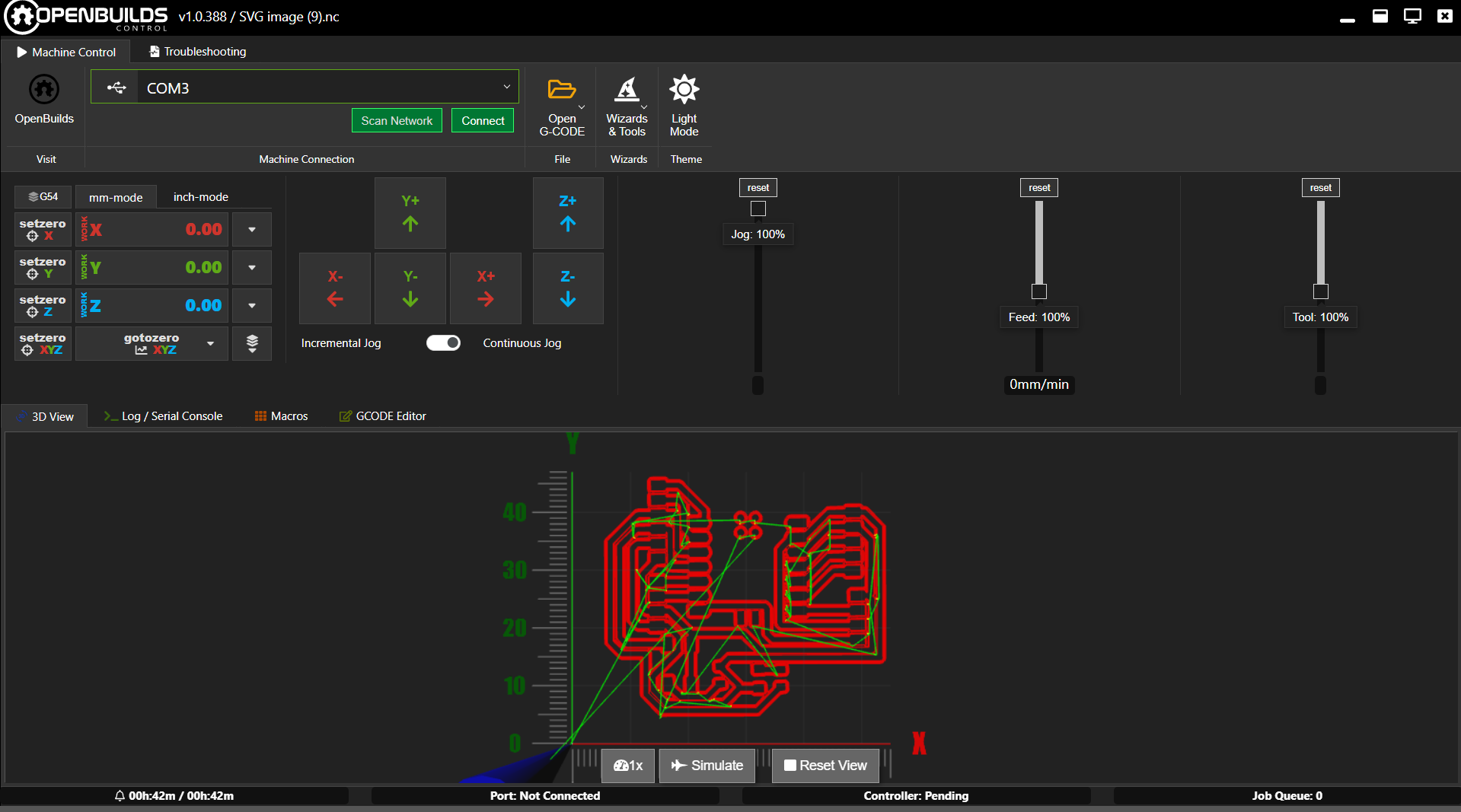
Milling the Circuit Board
The G-code file was then imported into the OpenBuilds Control CAM software, which interfaces with the CNC milling machine to execute the board fabrication.
Steps to mill
- Open the OpenBuilds Control CAM software.
- Import the G-code trace file.
- Set the zero point, and cutting parameters (depth:0.1mm, speed:4mm/s, tool type: V-bit-tip:0.1mm-angle:30).
- Send the job to the milling machine.
The visualization of the circuit board is to confirm that all traces are well marked before milling.
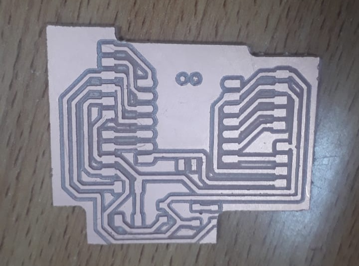
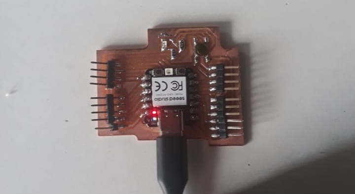
Final PCB Output
Here are images of the PCB immediately after milling, before and after soldering the components:
Milled PCB (Before Soldering)
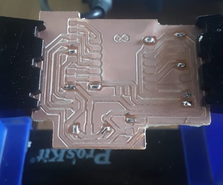
Assembled PCB (After Soldering)
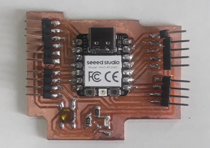
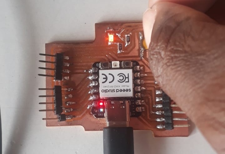
Testing the Circuit
To verify the functionality of the board:
The microcontroller was powered via USB.
When the push button was pressed, the LED successfully turned on, indicating proper connectivity and soldering.
The bellow code used to program microcontroller testing:
  #define BUTTON_PIN 12
  #define LED_PIN 13 //the XIAO RP2040 LED pin is connected to Pin 13

  void setup() {
    pinMode(BUTTON_PIN, INPUT_PULLUP);
    pinMode(LED_PIN, OUTPUT);
  }

  void loop() {
    if (digitalRead(BUTTON_PIN) == LOW) {
      digitalWrite(LED_PIN, HIGH);
    } else {
      digitalWrite(LED_PIN, LOW);
    }
  }
Test Video
Design files
Schematic
PCB
SVG Gerber
PCB Cut F.cu