Week 6 assignment
This week covers the design of the circuit board using EDA tool. The design covers from schematic design to complete (Printed Circuit Board) PCB.
The group assignment covers the test using lab equipment and observe the operations of the micro-controller circuit board.
This is the link for group assignment: Group assignment
Why choosing Seed Xiao ESP32 and RP2040
The Seeed XIAO ESP32 + RP2040 is a unique combination of two popular micro-controllers: the ESP32 and the RP2040. Choosing this board comes with several advantages, depending on the project requirements. Here are some key reasons why considering using it:
For the assignment I will be using Seed Xiao RP2040 micro-controller.
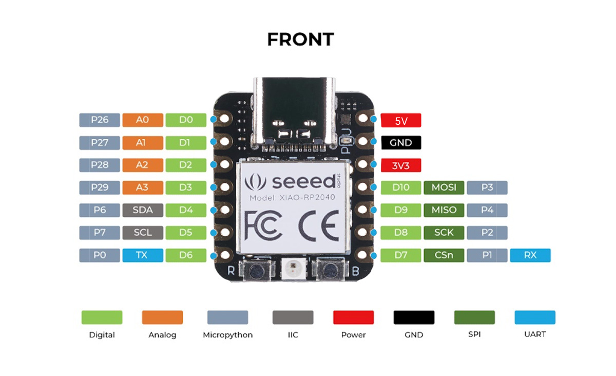
- Dual Microcontroller Architecture (ESP32 RP2040): ESP32: A powerful microcontroller that includes Wi-Fi, Bluetooth, and has substantial processing power with dual-core architecture (up to 240 MHz), making it ideal for projects requiring wireless connectivity and multi-tasking. RP2040: A flexible, low-cost microcontroller designed by Raspberry Pi. It features a dual-core ARM Cortex-M0+ processor and provides excellent processing power for handling low-level tasks and controlling sensors and peripherals efficiently.
- Compact Form Factor: The XIAO ESP32 RP2040 board is very compact, which makes it suitable for space-constrained projects. Despite its small size, it offers a lot of functionality. This is ideal for wearable devices, small robots, or any project where size is a critical factor.
- Wi-Fi and Bluetooth Support: The ESP32 onboard provides Wi-Fi and Bluetooth capabilities, which opens up a wide range of use cases. You can easily connect your project to the internet, use Bluetooth for communication with mobile apps, or create IoT (Internet of Things) devices. This makes it suitable for projects like remote monitoring, smart devices, home automation, and wearables.
- GPIO Pins: The XIAO ESP32 RP2040 offers a good number of GPIO pins, making it suitable for handling multiple sensors, actuators, and peripherals. It includes analog inputs, digital I/O, and PWM outputs. This is helpful for interfacing with sensors like temperature sensors, moisture sensors, motion detectors, motors, and more.
- Low Power Consumption: The ESP32 and RP2040 both support low-power operation, which is useful for battery-powered applications. The RP2040 especially has several power-saving modes, which helps extend the battery life for IoT devices. This is ideal for projects like remote weather stations, sensors, or wearable gadgets that need to run for extended periods without constant charging.
- Great for Embedded Projects: RP2040 is designed for low-level embedded applications, and with the added capabilities of the ESP32, it offers an all-in-one solution for embedded projects that require both local control and wireless communication. Projects involving embedded sensors (like temperature or moisture sensors) or real-time data processing (like motor control or robotics) can benefit from this combination.
- Versatile Development Environment: The XIAO ESP32 RP2040 is fully compatible with the Arduino IDE, which is a very popular platform for prototyping and rapid development. You can easily write and upload code using the familiar IDE, and the board also supports MicroPython for those who prefer Python over C/C++ for development.
- Economical: It provides a good balance between cost and features. The combined power of the ESP32 and RP2040 at a reasonable price makes it a great option for hobbyists, students, and engineers working on prototypes or low-cost devices. This affordability allows for experimentation and development without a large financial commitment.
- Community Support: Both the ESP32 and RP2040 have large and active communities. This means you can find plenty of tutorials, documentation, example codes, and troubleshooting tips online. It’s easier to get started and resolve issues thanks to a large user base.
- Flexible with Libraries and Tools: Allow access to a wide range of libraries for sensors, displays, motor drivers, and other peripherals. This simplifies development since many commonly-used libraries are already optimized for ESP32 and RP2040 platforms.
- Support for Advanced Features: ESP32 allows you to implement more advanced features like web servers, MQTT communication, cloud integration, audio processing, and even machine learning with the right libraries. You can also integrate camera modules, motion detection, or data logging with the cloud, thanks to the ESP32's wireless capabilities.
Datasheet link Seeed XIAO-RP2040
Individual assigment
I have used KiCAD downloaded from KiCCAD and installed.
I have installed KiCAD libraries to use in design of the circuit board, they are found in Fab Library
- Installation Procedures.
- Open PCB Editor (PCBNew).
- Click Tools → Update PCB from Schematic.
- Place components on the board.
- Move components to optimize placement.
- Define the board outline using Edge.Cuts layer.
- Select Route → Interactive Router.
- Connect components using traces (0.8mm).
-Make sure you have at least KiCad 8 or greater installed.
-Clone or download this repository. You should rename the directory to fab.
-Store it in a safe place such as ~/kicad/libraries or C:/kicad/libraries.
-Run KiCad or open a KiCad .pro file.
-Go to "Preferences / Configure Paths" and add new environment variable "FAB" that points to location of the fab library on your drive, e.g. ~/kicad/libraries/fab. This is needed for the 3D models to load correctly.
-Go to "Preferences / Manage Symbol Libraries" and add fab.kicad_sym as symbol library.
-Go to "Preferences / Manage Footprint Libraries" and add fab.pretty as footprint library.
I opned the installed KiCAD software and created new project which will hold all the schematic and pcd designs.
On the schematic design, I used symble tool to add components that will be used to build the circuit board.
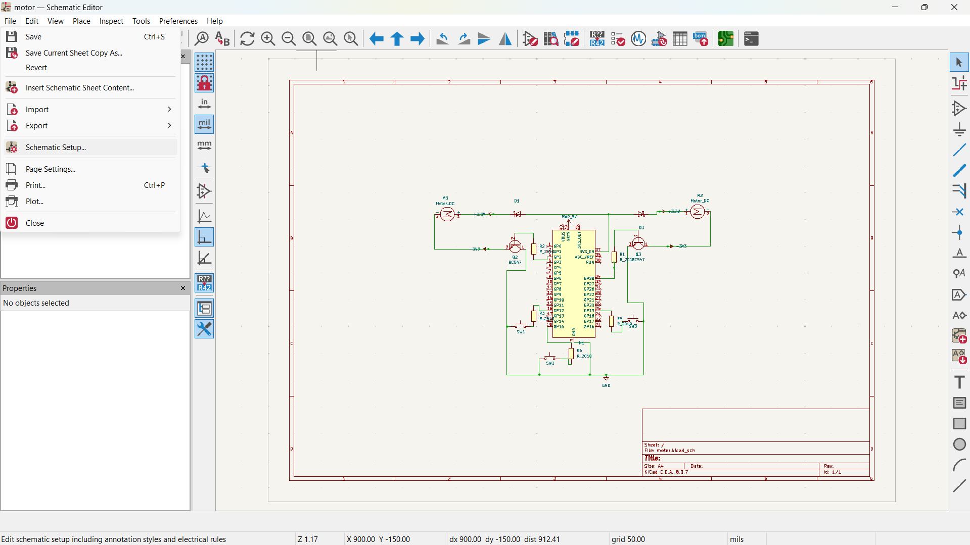
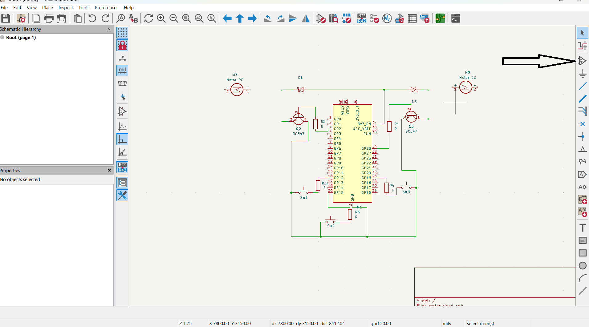
To generate the PCB I imported the chematic into the PBC Editor. The process is defined bellow.
Import Schematic into PCB Editor
Arrange Components and Define Board Shape
Route Traces
Screenshots bellow shows the PCB design and routing.
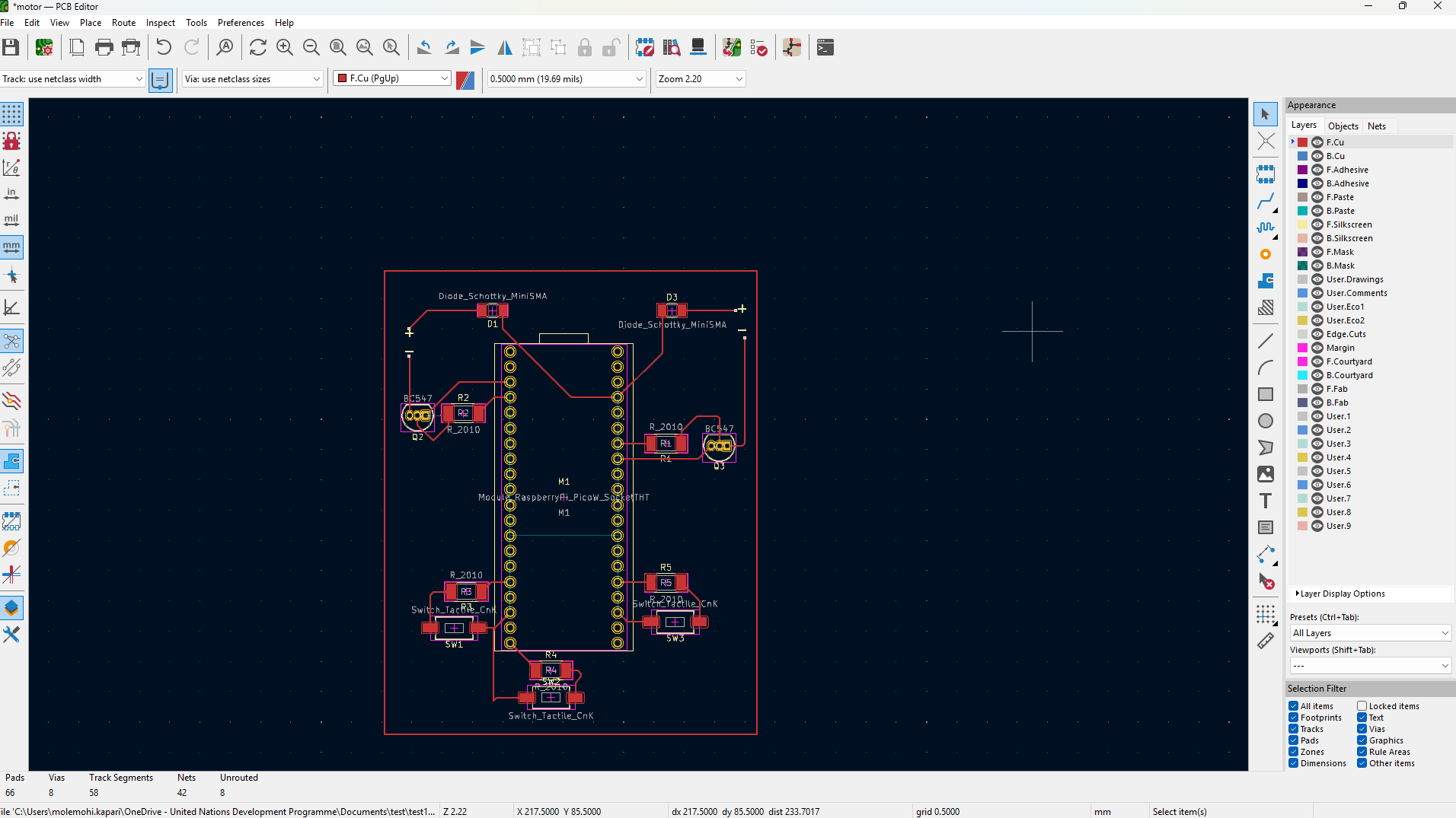
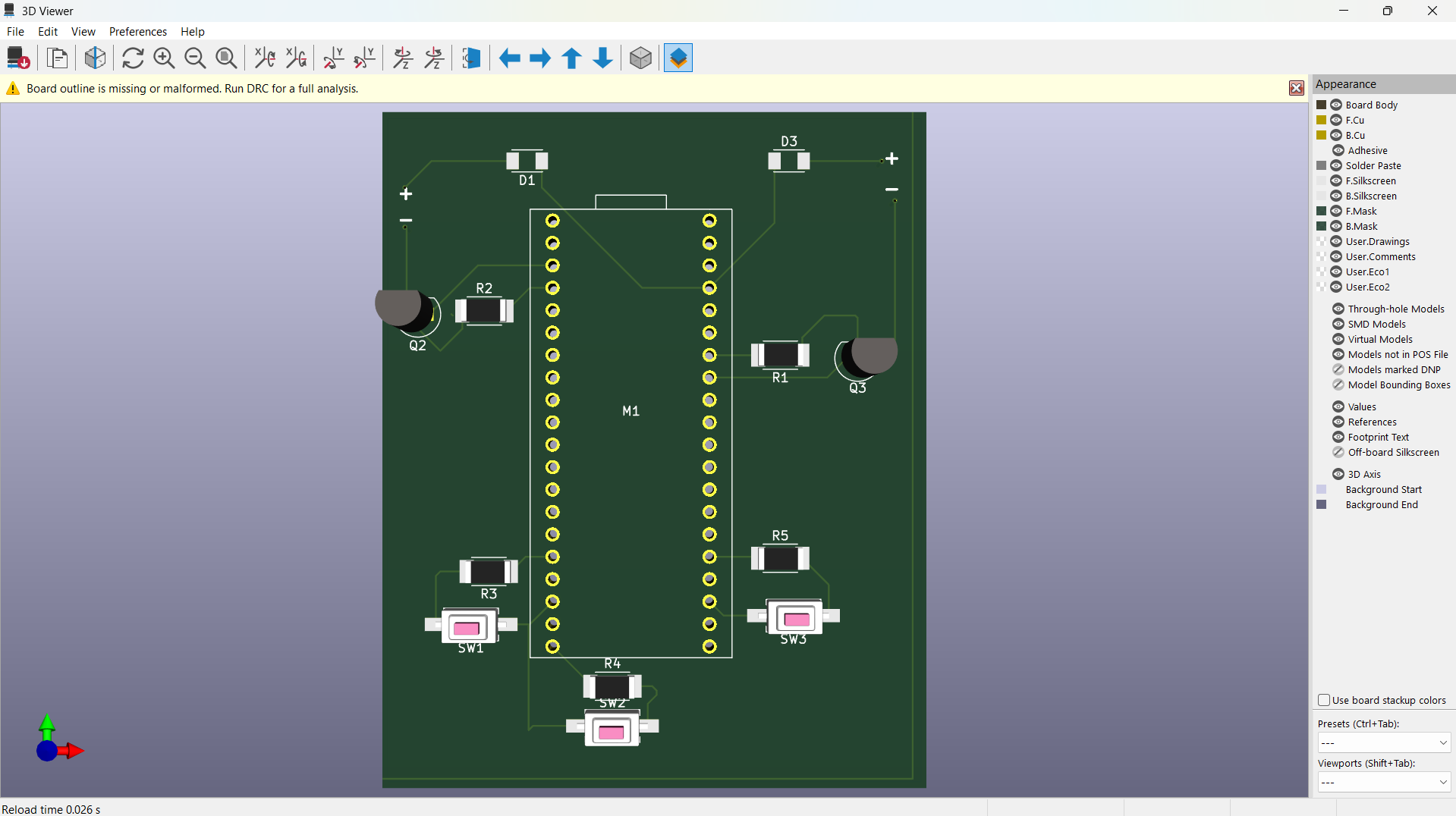
Bellow is the 3D view of the final product.
Design files
Schematic
PCB