Electronics Production
This week focuses on the process of fabricating and assembling printed circuit boards (PCBs). The objective is to understand the steps involved in milling, soldering, and testing custom-designed boards.
Group Assignment
- Characterize the design rules for your in-house PCB production process.
- Submit a PCB design to a board house.
Summary of Group Assignment
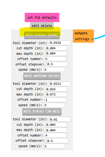
During this assignment, we focused on characterizing the design rules for in-house PCB production. We used the ROLAND SRM-20 milling machine, which provides high precision for PCB fabrication. Two main tools were used: a 15-degree V-bit for engraving and a 0.8 mm end mill with two flutes for cutting. We also analyzed critical parameters such as hole sizes, ensuring proper placement of vias and component mounting.
If you want to know more about what we did in the group assignment, click on this link: Group Assignment Details
Individual Assignment
- Make and test a microcontroller development board that you designed.
- A 5V regulator to control the SG90 servo motors.
- A 3.3V regulator to power the Xiao ESP32C3 and other connected components.
- Created a new project named “Final Board.”
- Opened the schematic editor and used the “Place Symbols” tool to add my components.
- Used labels to make connections instead of direct wiring. This improved readability and organization.
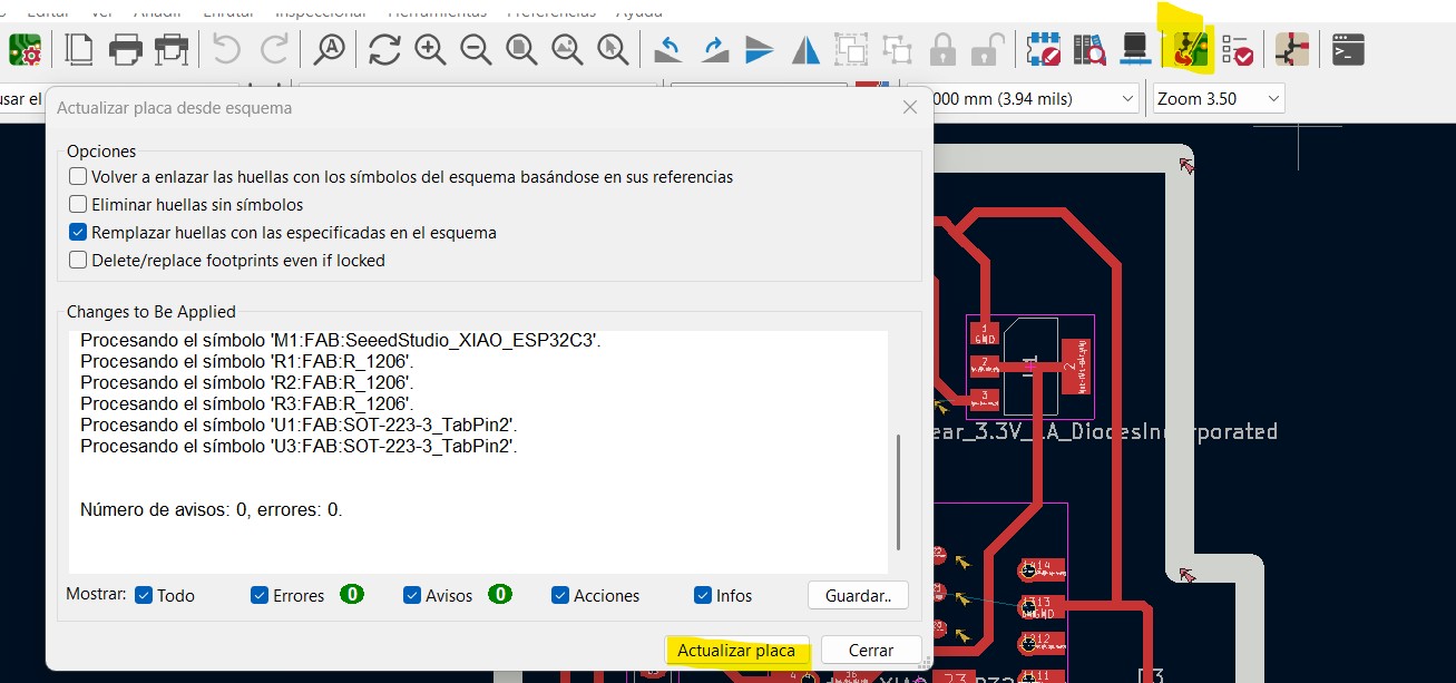
- Opened the PCB Editor in KiCad and imported the schematic components.
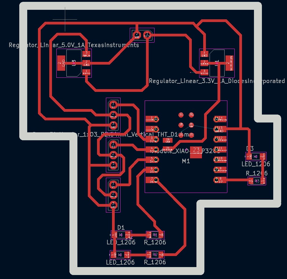
- Arranged the components, ensuring enough spacing between them for easier soldering and reduced interference.
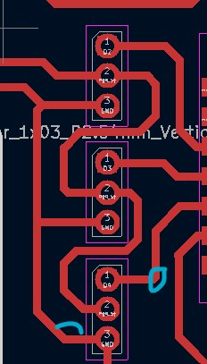
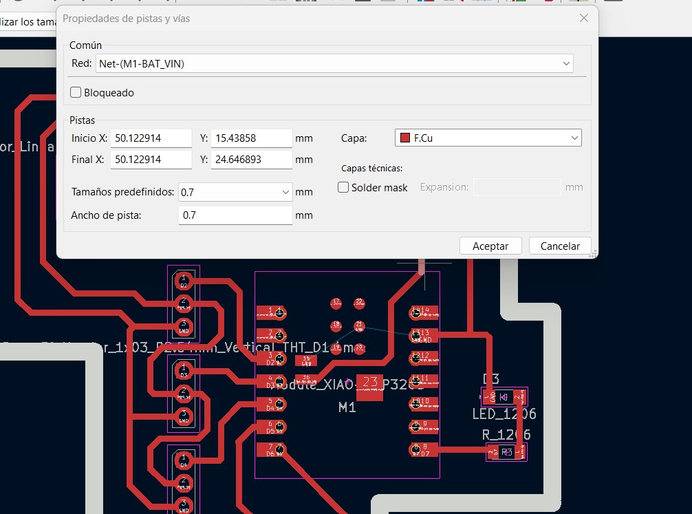
- Routed the traces, keeping them at a preferred 45-degree angle instead of 90 degrees for better signal flow.
- Set the trace width to 0.7mm to ensure proper current flow and minimize resistance.
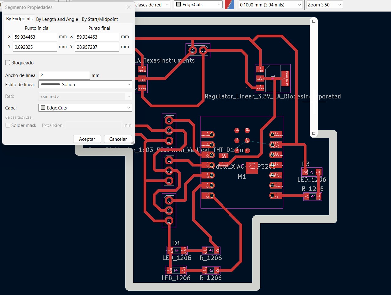
- Defined the board outline using the Edge Cuts layer with a thickness of 2.00mm.
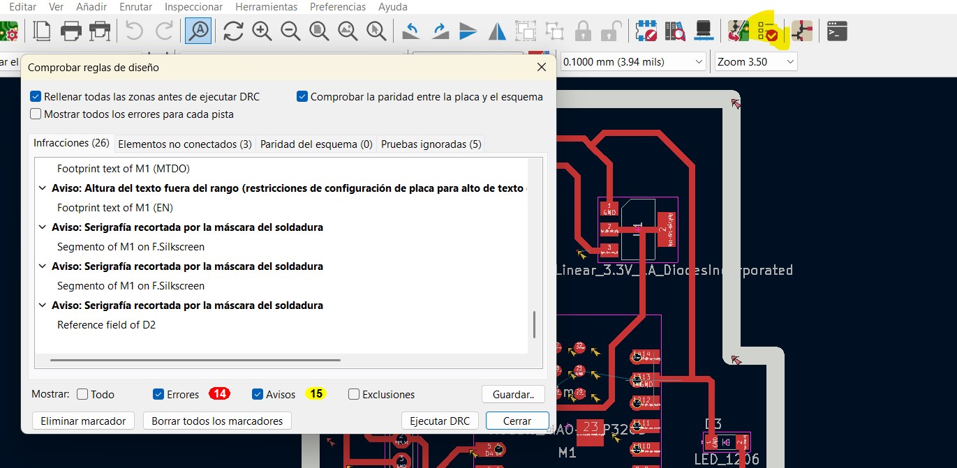
- Ran the Design Rule Check (DRC) to ensure no errors in the layout. It is possible that some errors may appear, but it is important to identify whether they are actually due to unused pins that are not connected or layers that you will not be using
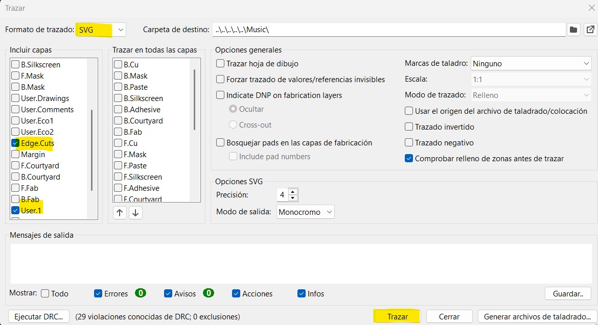
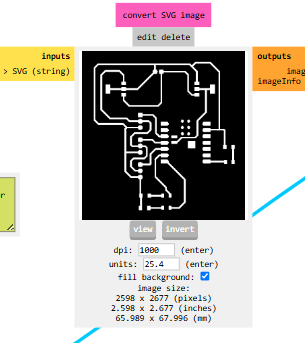
- Exported the SVG files for PCB fabrication.
Exported the SVG files for PCB fabrication. In KiCad 9, I used the Plot tool to generate the Gerber files. First, I opened the PCB Editor and navigated to File > Plot. Then, I selected the necessary layers, including F.Cu (Front Copper), Edge.Cuts, and User 1 (here I put my holes). I ensured the format was set to SVG and clicked "Plot" to generate the files.
NOTE: It is important to do the Plot , one by one , this because in the mods platform, which I will explain later on , nedd to do the gcode one by one , to put in the PCB cutter.
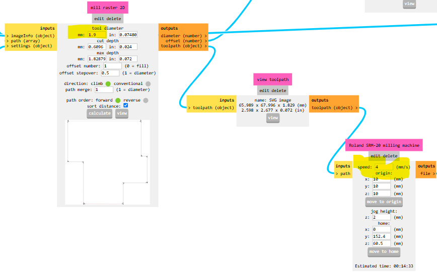
- Go to MODS Project.
- Click on Programs. Select Open Programs.Choose Roland MonoFab 2D PCB.
- Upload your SVG file.
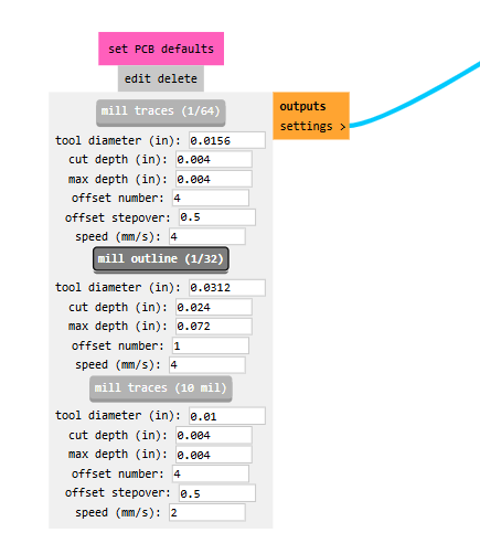
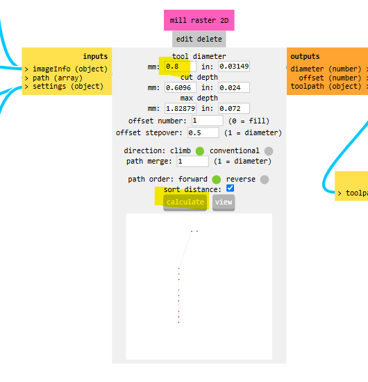
- Once the SVG file is ready, change the setting to Mills Outrace.
- Change the tool thickness to 0.08.
- Set the speed to 2.
- Click Calculate to generate the toolpath.
- Once the toolpath is verified, click the blue button to generate the file for the machine. Click Calculate again to start the download process.
- For the traces, follow the same process.
- Instead of selecting Mills Outrace, choose Mills Traces.
- Keep the tool thickness at 0.08 and the speed at 2.
- And at last , but not least , the Edge Cuts, follow the same process as the holes .
- Change the tool thickness at 1.9mm if your tool is 2.00mm and the speed at 4.
- The first tool was the cutting tool with a diameter of 0.8 mm, used for drilling holes and cutting the PCB outline.
- The second tool was a V-shaped engraving tool, used for milling the PCB traces.
- First, I calibrated the X and Y axes at the lower-left corner of the PCB.Then the Z-axis
- For large movements, I selected the “x10” option.
- For small, precise adjustments, I used the “X1” option.
- I clicked on the “Cut” option in VPanel.
- I selected my drill file and clicked on “Setup”.
- The machine began drilling the holes.
- Once the process was complete, I carefully removed the PCB from the sacrificial bed.
- I used fine sandpaper to smooth the edges.
- I cleaned the PCB with isopropyl alcohol to remove any remaining dust or oxidation.
- Prepare the PCB: Ensure the PCB is clean and free of dust or oxidation.
- Apply flux: Use a small amount of flux on the pads to improve adhesion and prevent oxidation.
- Heat the pad and component lead: Place the soldering iron tip on both simultaneously for a few seconds.
- Apply solder: Once the pad and lead are heated, add a small amount of solder and let it flow naturally.
- Remove the soldering iron: Gently lift the iron away and let the solder joint cool undisturbed.
- Inspect the joint: Ensure the solder forms a smooth, shiny connection.
- Clean the board: Use isopropyl alcohol and a brush to remove excess flux residue.
- Ensure the soldering iron is at the correct temperature (350-400°C for most components).
- Use the right amount of solder; too much can cause short circuits, while too little may result in weak connections.
- Avoid overheating components, as excessive heat can damage sensitive parts.
- Work in a well-ventilated area to avoid inhaling flux fumes.
- Keep the soldering iron tip clean by regularly wiping it on a damp sponge.
- Microcontroller-based development boards.
- Open-source and widely supported by a large community.
- Uses the Arduino IDE for programming in C/C++.
- Compatible with multiple sensors, actuators, and communication modules.
- Download and install the Arduino IDE.
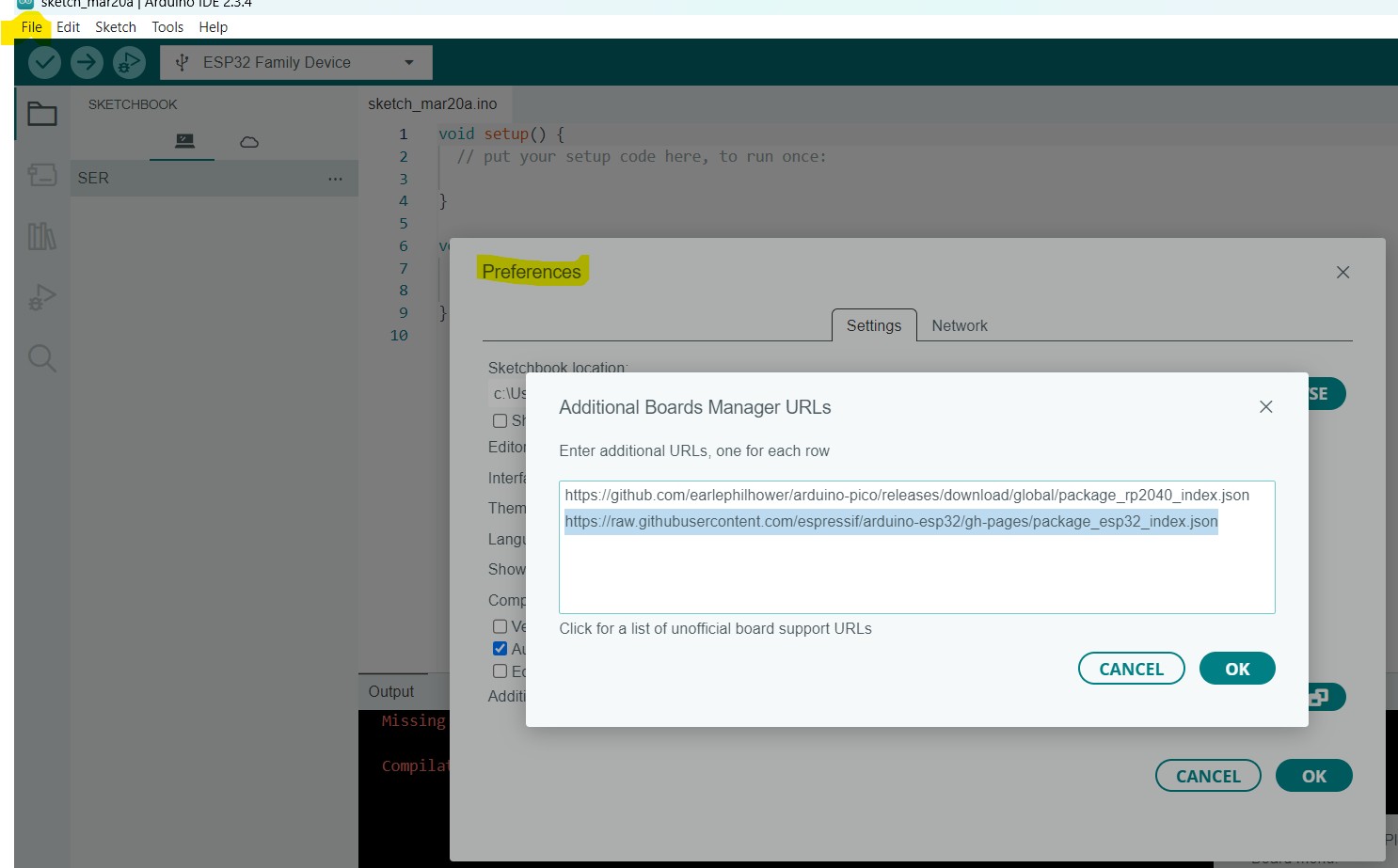
- Open Arduino IDE and go to File > Preferences.
- In the "Additional Boards Manager URLs" field, add this URL:
https://dl.espressif.com/dl/package_esp32_index.json
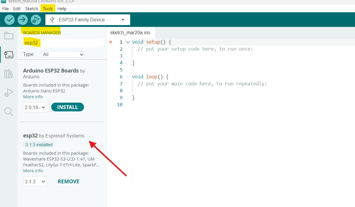
- Go to Tools > Board > Board Manager, search for "ESP32" and install the "ESP32 by Espressif Systems" package.
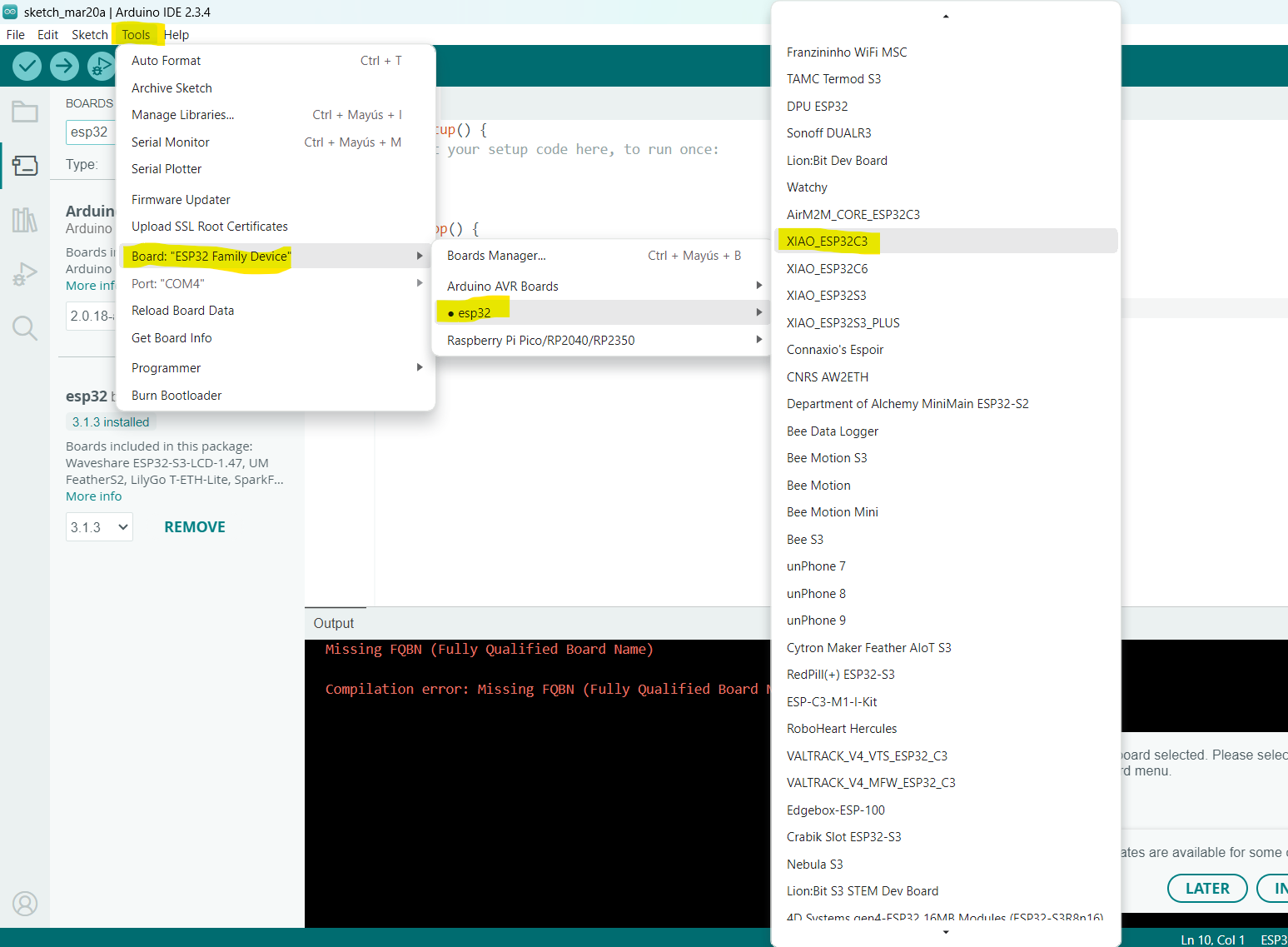
- Select your Xiao ESP32 board by going to Tools > Board and choosing the correct model.
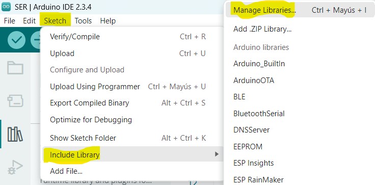
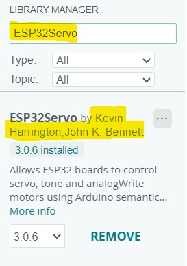
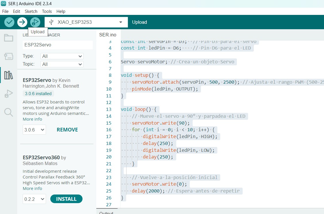
- Go to Sketch > Include Library > Manage Libraries.
- Search for ESP32Servo and install it by Kevin Harrington
- Ensure the ESP32 support library is installed.
- The servo motor is connected to pin D2 and the LED to pin D4.
- In the setup section:
- The LED pin is set up as an output.
- The servo is attached to its pin and moves to the starting position (0 degrees).
- In the loop section:
- The servo moves to 90 degrees and the LED turns ON for 500 milliseconds.
- Then, the servo moves back to 0 degrees and the LED turns OFF for another 500 milliseconds.
- This cycle repeats indefinitely, making the servo move back and forth while the LED blinks.
- Connect your Xiao ESP32 to your computer via USB.
- Click on the Upload button.
- Your servo motor should start moving with the LED blinking each time.
- Improving schematic design by using labels instead of direct wiring for better readability.
- Mastering the use of KiCad for PCB layout, component selection, and Design Rule Checking (DRC).
- Generating proper Gerber files and SVG exports for PCB milling using MODS Project.
- Operating the Roland MonoFab SRM-20 for precision milling, including tool selection and calibration.
- Understanding common challenges, such as tool slipping during edge cutting, and exploring alternative solutions.
- Implementing servo motor and LED control using the Xiao ESP32, reinforcing microcontroller programming skills.
- Files
This week, we worked again with KiCad.
What is KiCad?
KiCad is an open-source software suite for Electronic Design Automation (EDA). It allows users to create schematic diagrams and design PCB layouts. It is widely used for designing custom electronics. You can download KiCad from the official website: KiCad Download.
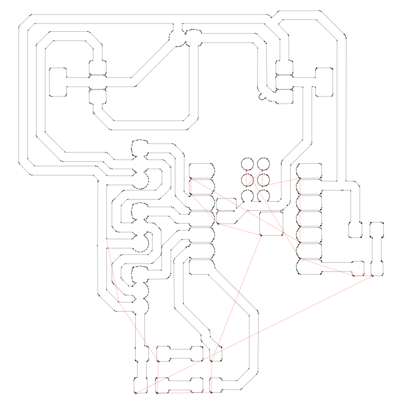
Designing My PCB
In week 6, we used KiCad to design our PCBs. Although I already had a design, I decided to redo it because I was not satisfied with the previous version. The connections were confusing, and the board was not very practical. This time, I improved the schematic and the board layout.
Before
After
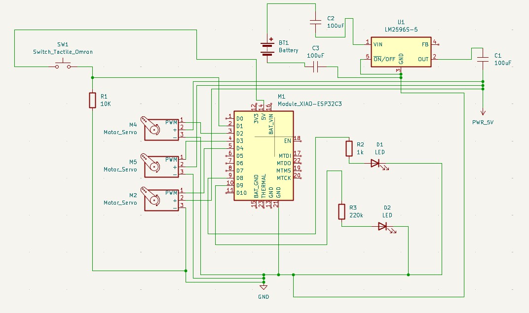
For my final project, I need to control three motors and communicate via Bluetooth. Therefore, I designed a PCB using the Xiao ESP32C3.
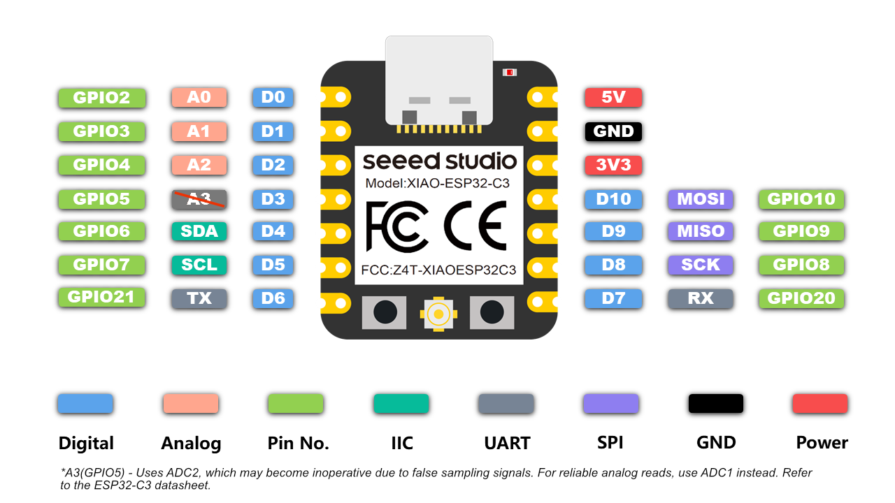
Component Selection
To power the motors, I added two voltage regulators:
I also included three LEDs to indicate which motor is active. The board is powered by a 7.4V battery. The battery is not directly attached to the board, but I added holes to solder pins, allowing for an external battery connection.
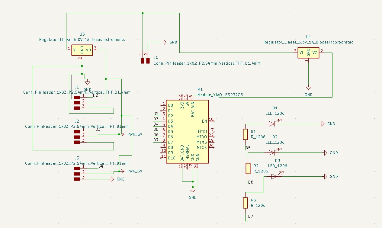
PCB Design Process
I followed the same steps as in week 6 to design my board in KiCad, but I used labels instead of direct wire connections. This made the schematic more organized and easier to understand.
Steps:
Once the schematic was complete, I proceeded to the PCB editor. The improved organization made routing the connections much easier.
PCB Layout Steps in KiCad
After completing the schematic, I proceeded to design the PCB layout. Below are the steps I followed:
How to Use MODS Project for PCB Milling
The MODS Project is an online tool for generating toolpaths for PCB milling and other fabrication processes.
Steps to Generate a PCB File for Roland MonoFab
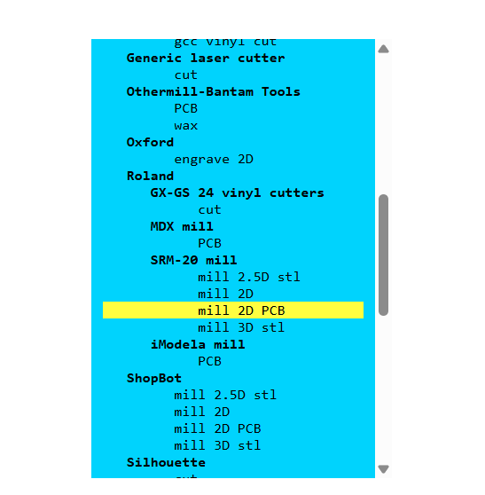
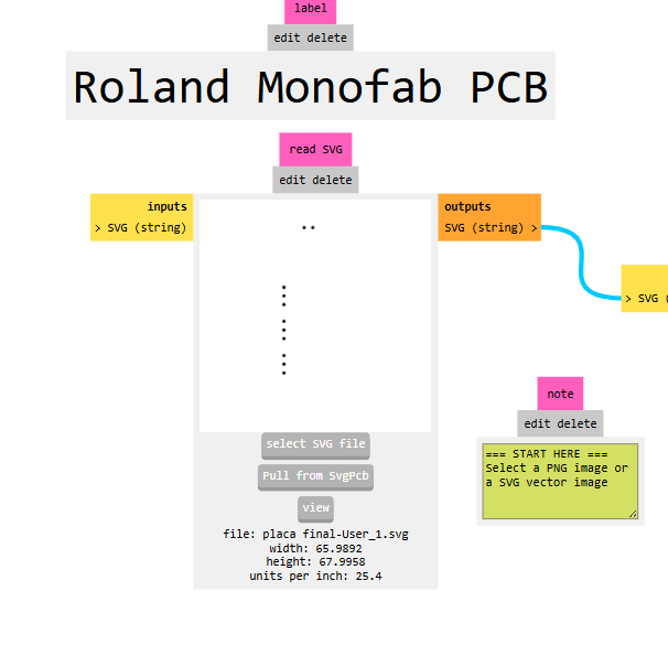
Start with the holes, then the traces, and finally the edge cuts.The process for holes and edge cuts is the same.

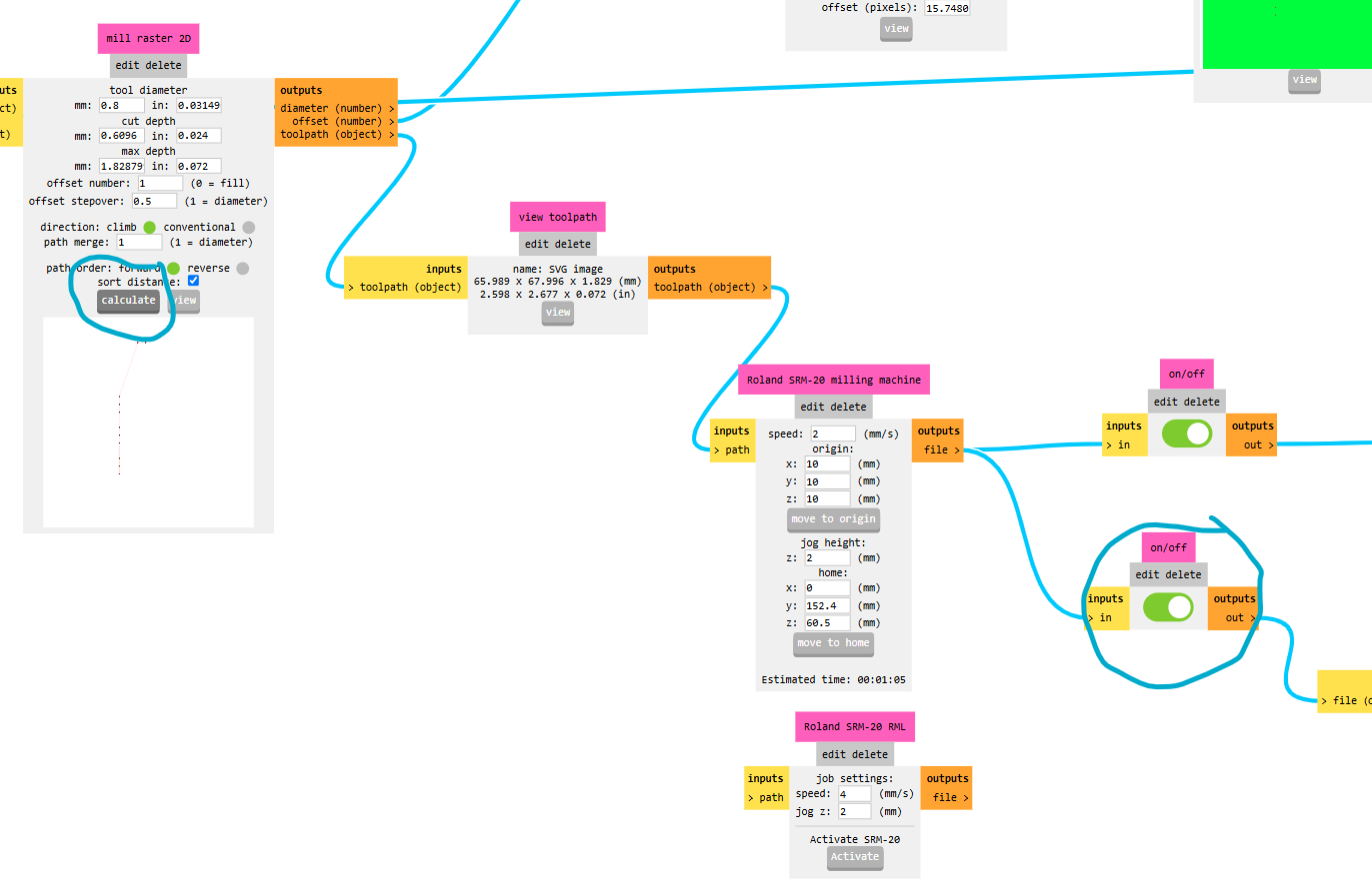
Traces
To do the traces its important to invert the image, so the machine cut the parts in black , and not the parts in white
Edge Cuts
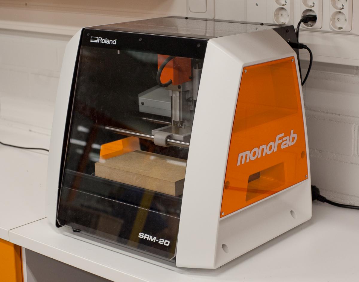
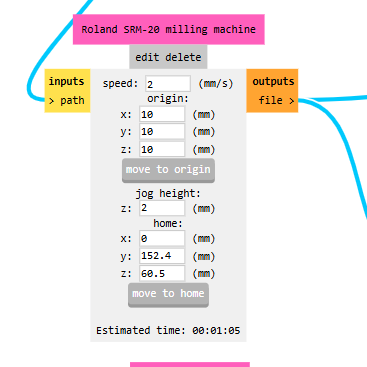
Steps to Use the Roland MonoFab SRM-20 for PCB Milling
1 Installing and Setting Up the Machine
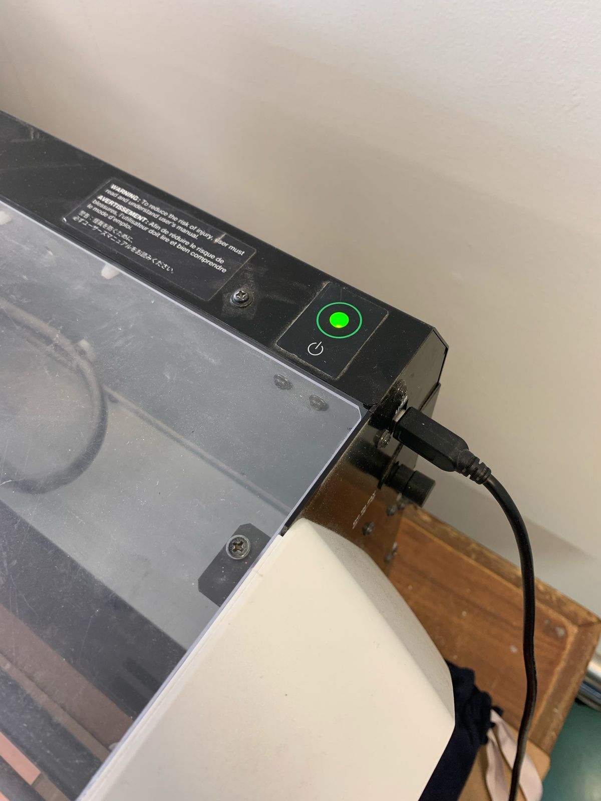
First, I installed the VPanel software for the machine (VPanel for SRM-20) and connected my computer to the Roland MonoFab SRM-20.
Then, I turned on the machine and verified that it was properly connected.
2 Preparing the Work Area
Next, I used a sacrificial bed made of MDF to protect the milling surface, and I placed my copper PCB on top of it.
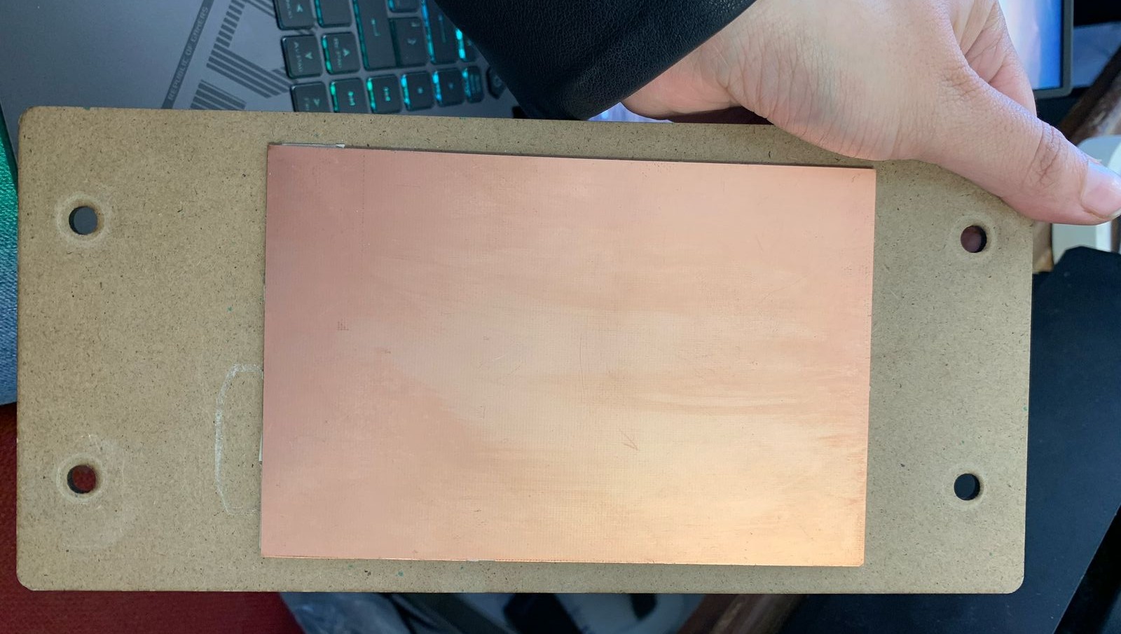
After that, I secured the sacrificial bed inside the machine and adjusted it using screws.
3 Choosing and Installing the Tools
I checked the tools that I was going to use:
I started by placing the first tool and securing it properly using a star-shaped screwdriver.
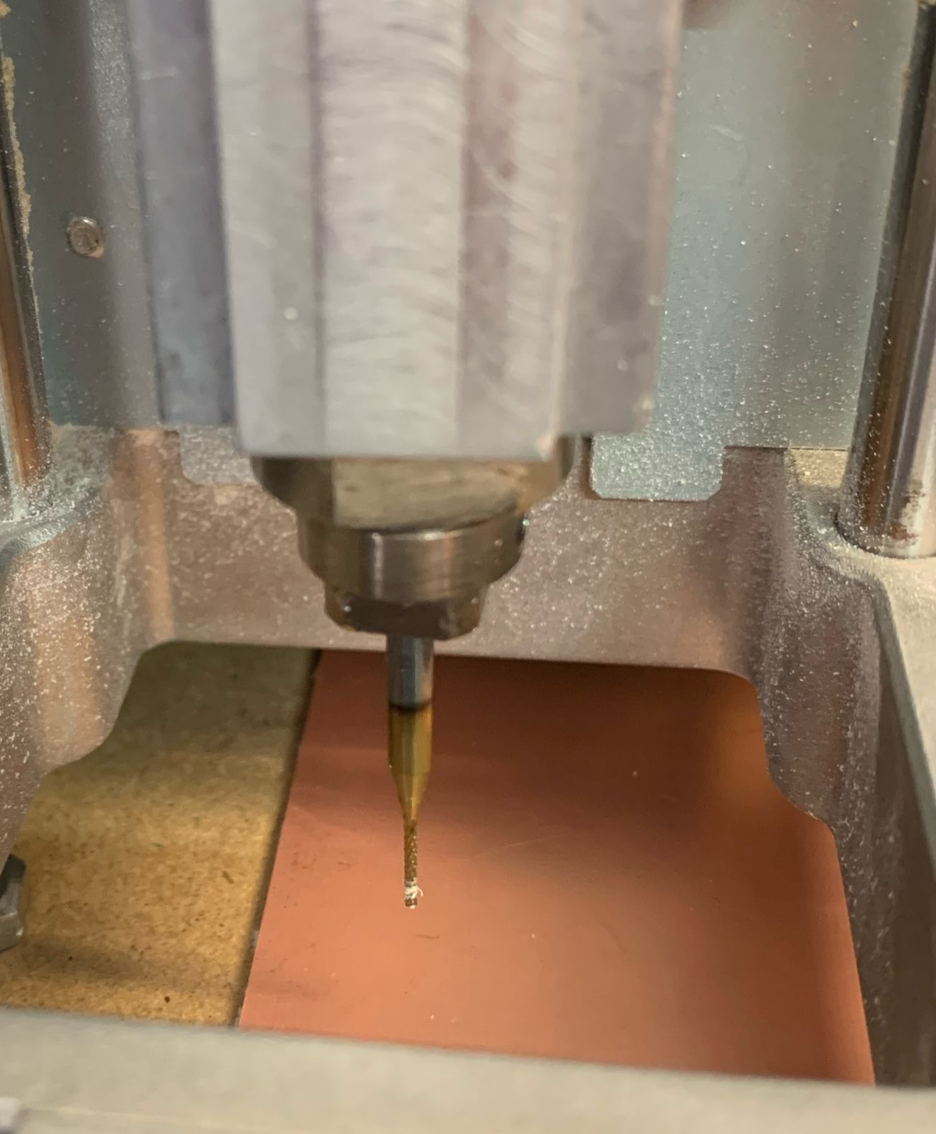
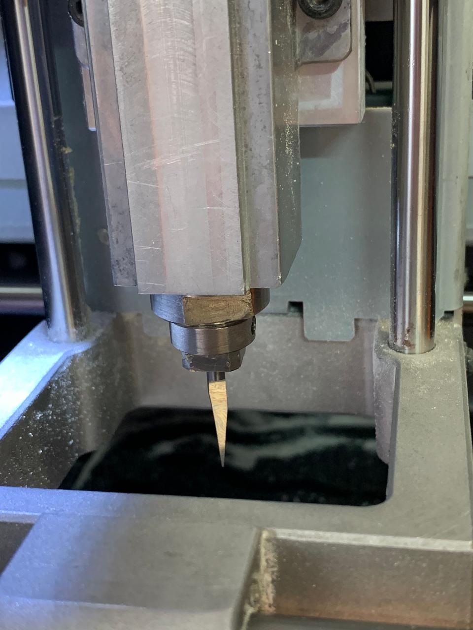
4 Calibrating the Machine
Before milling, I needed to calibrate the machine axes:
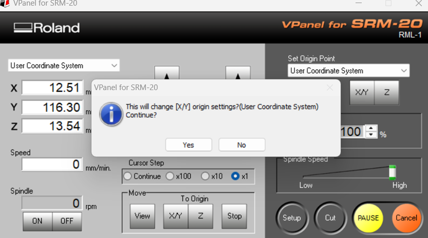
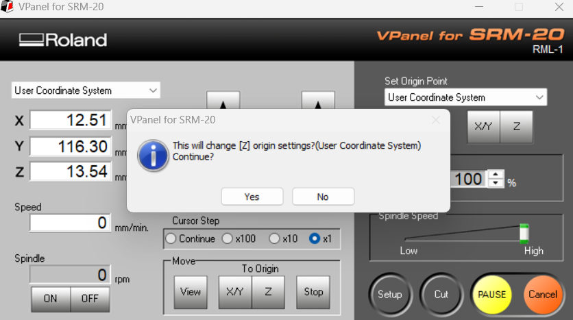
To move the tool correctly, I used the movement buttons in VPanel:
To verify that the tool was cutting only the required area, I placed the tool at the origin and clicked on the “Z” and “X/Y” options to return to the set axes. Then, I moved to the Spindle section and turned it on.
Important: Only the tool should touch the copper plate; otherwise, it could engrave or cut deeper than needed.
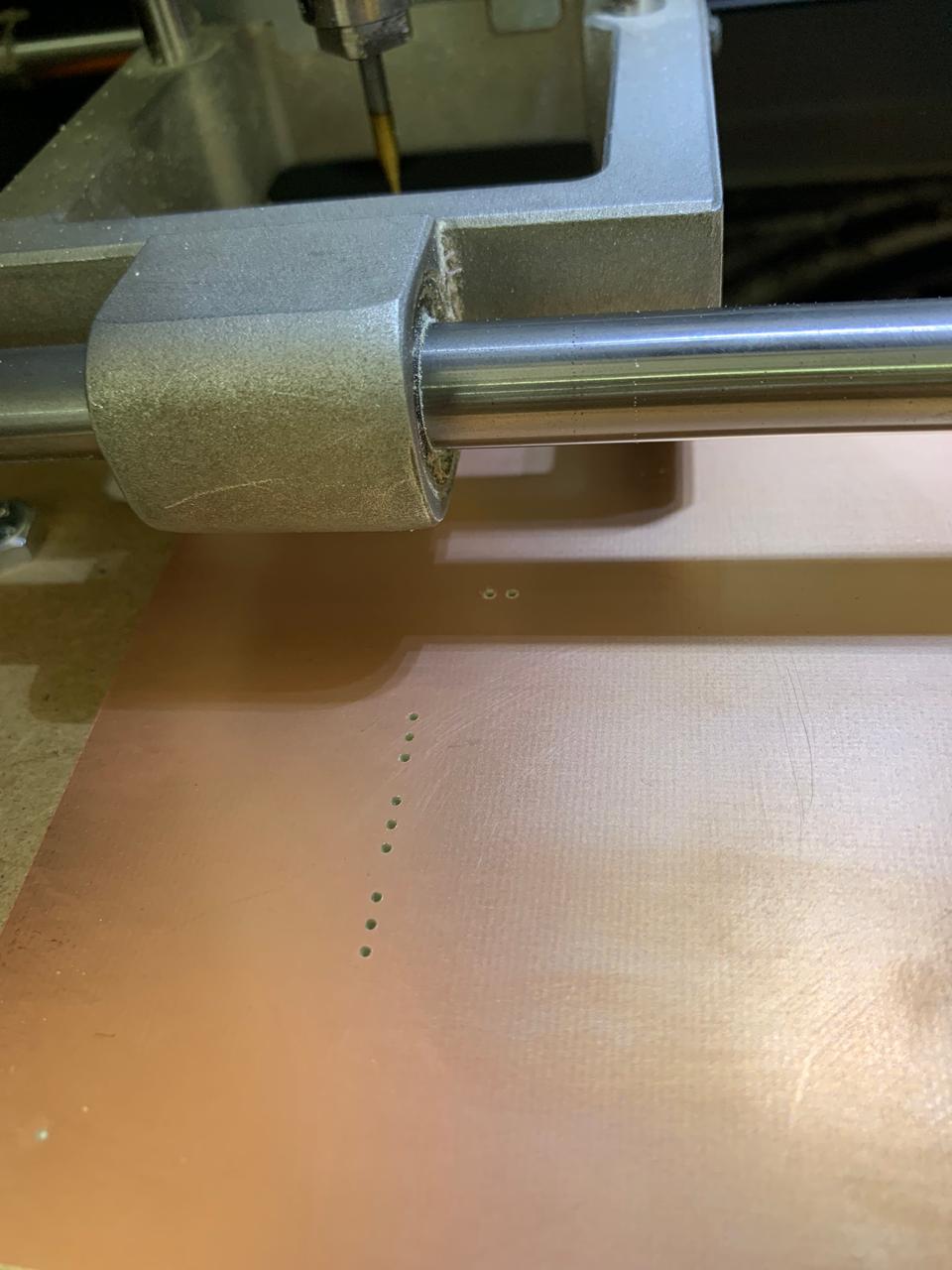
5 Drilling the Holes
First, I started with the drilling process using the cutting tool.
6 Engraving the PCB Traces
Once the holes were done, I replaced the cutting tool with the engraving tool.
Because I changed the tool, I needed to recalibrate the Z-axis again to ensure proper engraving depth.
Then, I started the engraving process.
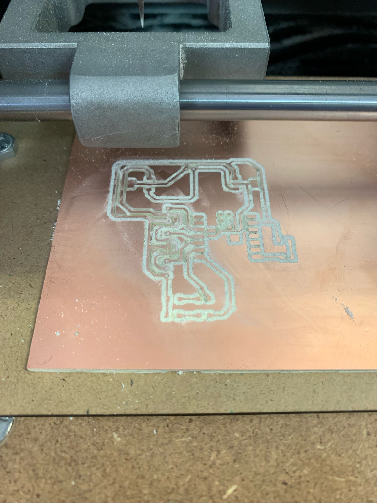
7 Removing Dust and Residue
During the milling process, copper and fiberglass dust accumulate. To clean the surface, I used a vacuum cleaner to remove all the debris.
8 Removing and Cleaning the PCB
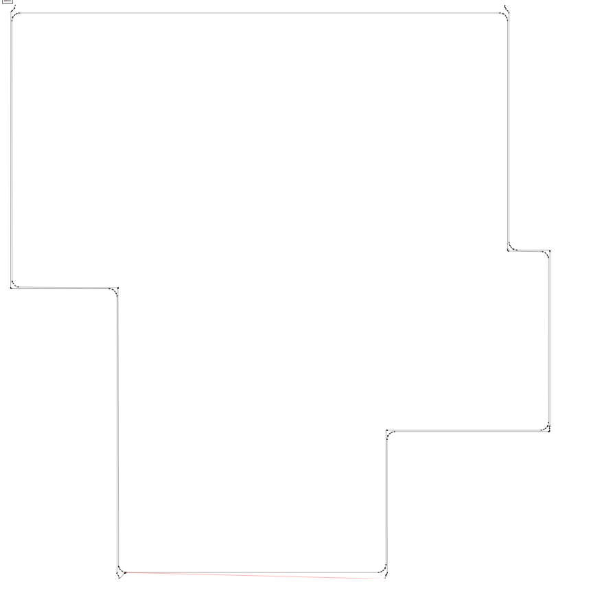
9 Cutting the PCB Outline
Finally, I switched back to the cutting tool to mill the PCB outline.
During thhe cutting of the pcb outline, I had issues with the tool, the tool wasn't tight enough, and duroing te cuts, this one falls down very often, so I decided to cut the PCB Outline Manually
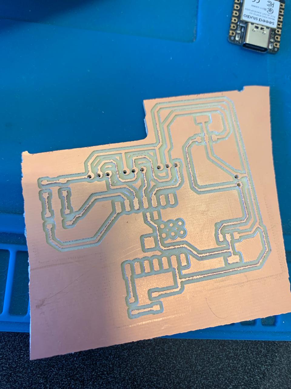
I Know i'ts not the best cut of edges ever , but I will improve it.
Additional Tip: Manual Cutting Option
If you face issues with the milling process, especially when cutting the edge cuts, and the machine pauses or restarts frequently, you may consider manually cutting the PCB with a saw. While it's not the preferred method, this can prevent damage to the milling tool and ensure better control over the cut.
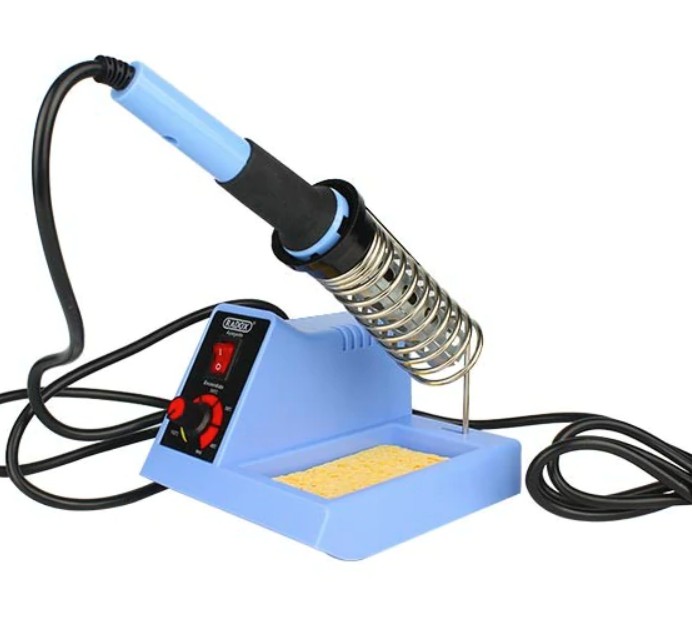
10 Soldering the Components
After cutting the PCB, I proceeded to solder the components onto the board. I used soldering tin, a soldering iron set to 350-400°C (662-752°F), and flux for a better soldering process.


Steps for Soldering the Components:
Tips for Better Soldering:
Step-by-Step Guide for Servo Motor and LED Control with Xiao ESP32
What is Arduino?
Arduino is an open-source electronics platform based on easy-to-use hardware and software. It is widely used for creating interactive projects, from simple LED blinking to complex IoT applications.
Key Features of Arduino:
Getting Started with Arduino:
To start working with Arduino, follow these steps:
Step 1: Set Up the Arduino IDE for Xiao ESP32
Step 2: Install Necessary Libraries
Step 3: Code for Servo and LED Control
This code controls a servo motor and an LED using an Arduino board.
How It Works:
See the Pen Untitled by Paula Rivero (@Paula-Rivero) on CodePen.
Step 5: Upload the Code to Xiao ESP32
Learning Outcome
This week, I deepened my understanding of PCB fabrication, from designing in KiCad to milling and assembling custom development boards. Key takeaways include:
Overall, this assignment strengthened my skills in electronics production, bridging the gap between PCB design and physical implementation.
Documents