Electronics Design
This week, we will explore the design and analysis of electronic circuits focused on microcontrollers. Through hands-on exercises and computer-aided design (EDA) tools, we will learn how to create and evaluate custom development boards using components available in the lab inventory.
Group Assignment
We used test equipment to analyze the operation of a microcontroller circuit board, allowing us to better understand its behavior and electrical characteristics.
In this activity, we explored the use of electronic measurement tools such as the multimeter and oscilloscope to analyze the behavior of a circuit based on the XIAO RP2040. Through different tests, we verify the power supply of the microcontroller, the continuity of connections, and the generation of PWM and sinusoidal signals. This exercise helped us develop a better understanding of how to diagnose and validate electronic circuits. By using measurement tools effectively, we learned to identify power issues, verify signal integrity, and troubleshoot potential problems. This knowledge is crucial for ensuring that our custom PCB designs function correctly before manufacturing.
For more details, visit the Group Assignment Page.
Individual Assignment
Each student will design a custom development board with an embedded microcontroller, ensuring it can interact and communicate with other devices.
This week represents a crucial step in developing skills for creating custom hardware, combining theory, design tools, and experimental validation.
Development Board Design
In this stage, we will focus on designing a development board using Electronic Design Automation (EDA) tools. An EDA tool is software that enables the creation, simulation, and documentation of electronic circuits, making it easier to develop schematics and design Printed Circuit Boards (PCBs). These tools are essential for turning an idea into a functional circuit ready for manufacturing.
Using KiCad
For this project, I will use KiCad, a powerful and open-source electronic design tool. With KiCad, I will design the circuit schematic, define the layout of components on the PCB, and generate the necessary files for manufacturing. Additionally, I will explore the possibility of simulating the circuit before fabrication to optimize its performance and minimize errors.
You can download KiCad here.
Other EDA Software
Besides KiCad, there are several other EDA software options such as Eagle, Altium Designer, and EasyEDA. Each tool has its strengths:
| EDA Software | Free or Paid | Download Link | Key Features |
|---|---|---|---|
| KiCad | Free (Open-source) | Download KiCad |
|
| Eagle | Free for personal use (Paid for commercial use) | Download Eagle |
|
| Altium Designer | Paid (Subscription-based) | Download Altium Designer |
|
| EasyEDA | Free (Limited features), Paid for premium features | Download EasyEDA |
|
Importance of EDA Tools
Using EDA tools is a crucial step in hardware development, as they allow for the design of efficient circuits, proper component organization, and validation of the project’s feasibility before physical implementation.
PCB Design in KiCad
To design a PCB in KiCad, it is essential to understand its basic elements. Upon opening KiCad, we are presented with a menu that offers various functionalities, such as:
- Schematic Editor
- Symbol Editor
- PCB Editor
- Footprint Editor
- Gerber Viewer
- Image Converter
- Component Calculation Tools
- Worksheet Editor
- Content Plugin Manager
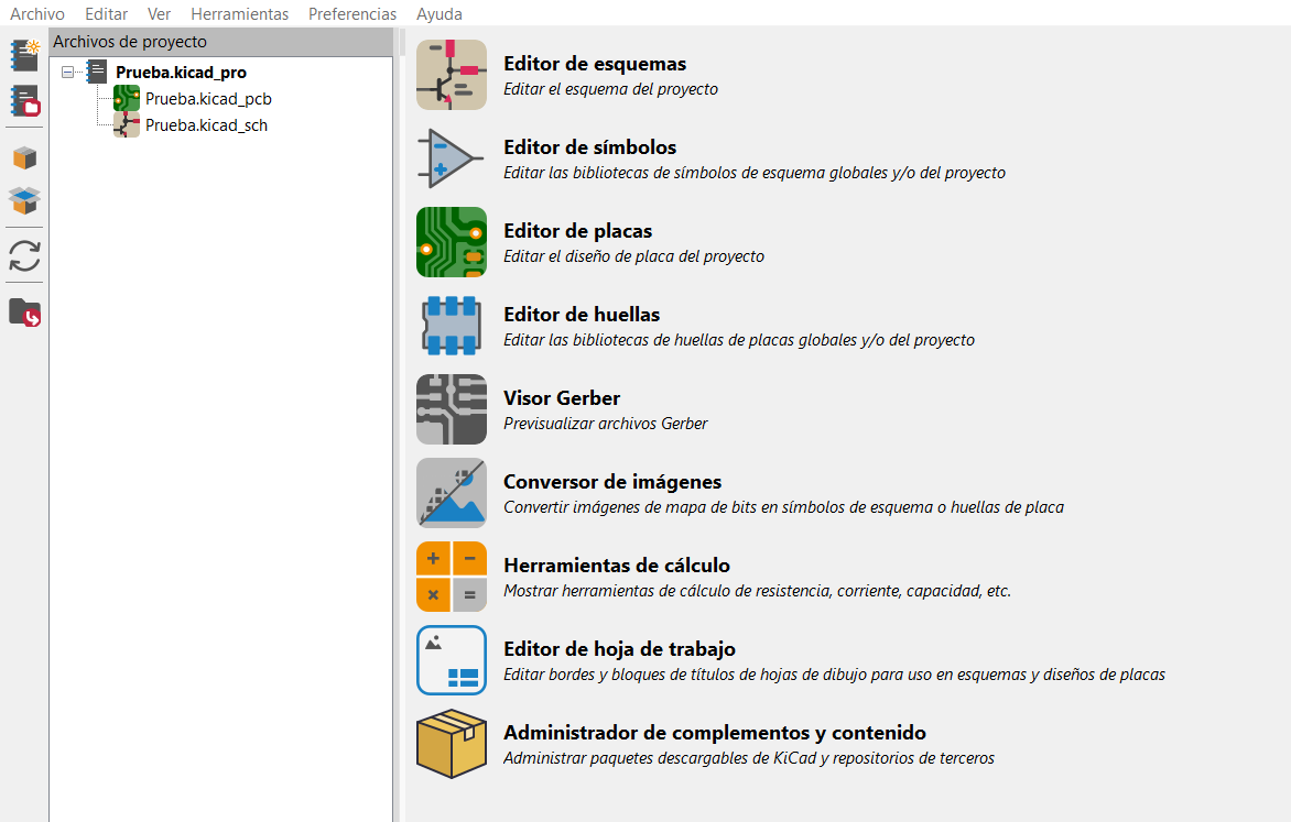
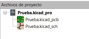
For this project, I will primarily use the schematic editor and the PCB editor. First, I create a new project, which automatically opens the schematic editor and PCB editor.
Schematic Editing
When opening the schematic editor, we see a workspace where key symbols are used. Some essential symbols in KiCad include:
- Resistors
- Capacitors
- Diodes
- Transistors
- Connectors
- Microcontrollers
In this section, components are highlighted in yellow. If additional components are needed, new libraries must be added. For guidance on library management, refer to the KiCad Manual.
Designing the PCB
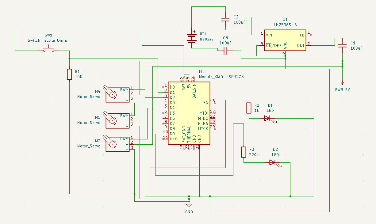
For my PCB, I took inspiration from my final project. The board includes the following components:
Microcontroller:
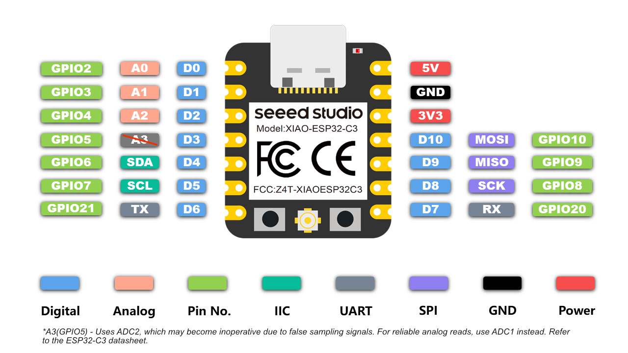
- 1x Seeed Studio XIAO ESP32C3
Actuators:
- 3x Servo Motors (SG90 or MG995)
LED Indicators:
- 1x LED (Motor Active Indicator) - D1
- 1x LED (Bluetooth Connection Indicator) - D2
Resistors:
- 2x 220Ω Resistors (for LEDs)
- 1x 10kΩ Resistor (for button - pull-down)
Button:
- 1x Push Button for manual motor control
Power Supply:
- 1x 5V External Power Source (for servos)
Wiring and Connections
I use the XIAO ESP32C3, locate the component, and place it on the schematic.
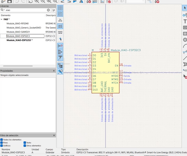
Next, I gather all necessary components, arrange them for clarity, and connect them accordingly.
Finally, I make the necessary connections by clicking on the component edges and drawing lines to establish electrical paths.
Final Schematic Design
And here is the final result of the connections.
Creating the PCB in KiCad
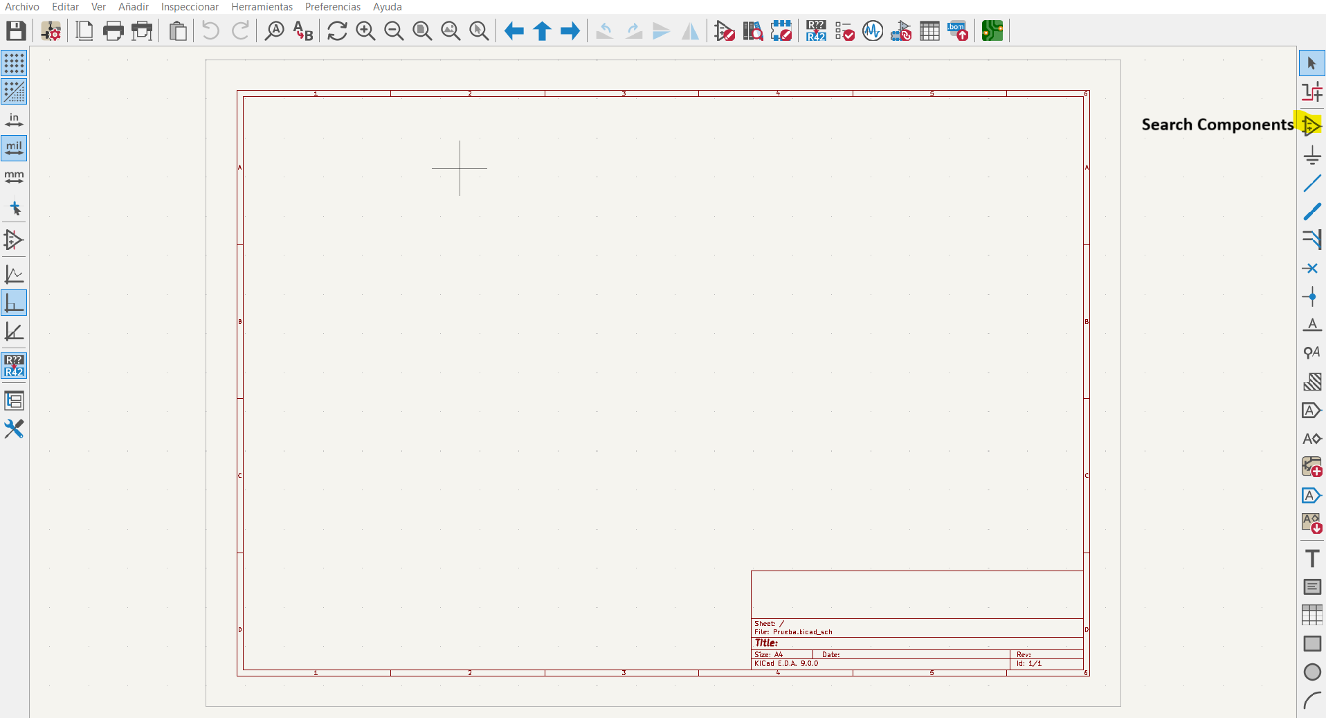
Now, we will create our PCB. To do this, we click on the PCB Editor button, located in the upper right menu, highlighted in yellow in the image below.

Assigning Footprints to Components
Before starting, it is important to ensure that our components have assigned footprints. To do this, follow these steps:
- Open the Schematic Editor and verify that all components are correctly connected.
- Click on "Assign Footprints to Components" in the toolbar.

- Select the appropriate footprint for each component (e.g., connectors, resistors, microcontrollers, etc.).
- Save and close the window.
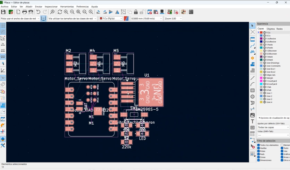
If everything is correct, the components will appear disorganized. In my case, they appeared like this:
Understanding Layers in KiCad
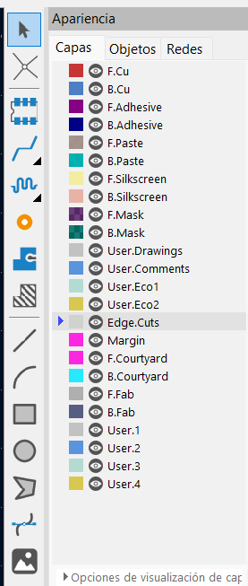
On the right side, we can see all the elements and layers visible in the design. Layers in KiCad help organize different aspects of the PCB layout:
- F.Cu (Front Copper): The top layer where components and traces are placed.
- B.Cu (Back Copper): The bottom layer for routing additional traces.
- Edge.Cuts: Defines the physical outline of the PCB.
- Silkscreen Layers (F.SilkS / B.SilkS): Used for component labels and markings.
- Solder Mask Layers (F.Mask / B.Mask): Define areas that will not be covered by solder mask.
Arranging Components and Routing Traces
Arrange the components as desired. This arrangement will determine how the PCB will look. Then, use the **Route Tracks** tool, highlighted in the image, to start making connections.
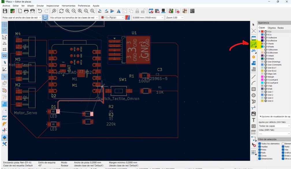
Now, draw the connection traces, following the blue lines.
Recommendations for PCB Routing
- Keep traces as short and direct as possible.
- Use wider traces for power and ground connections.
- Avoid 90-degree angles; use 45-degree angles instead.
- Ensure there is enough spacing between traces to prevent short circuits.
- Use a ground plane to improve signal integrity and reduce noise.
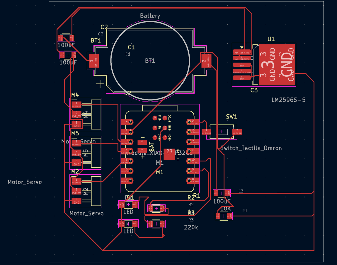
Final PCB Design
And here is the final PCB connections
Verifying the PCB Design
To verify that the PCB is correct, click on the **Design Rule Check (DRC)** button.
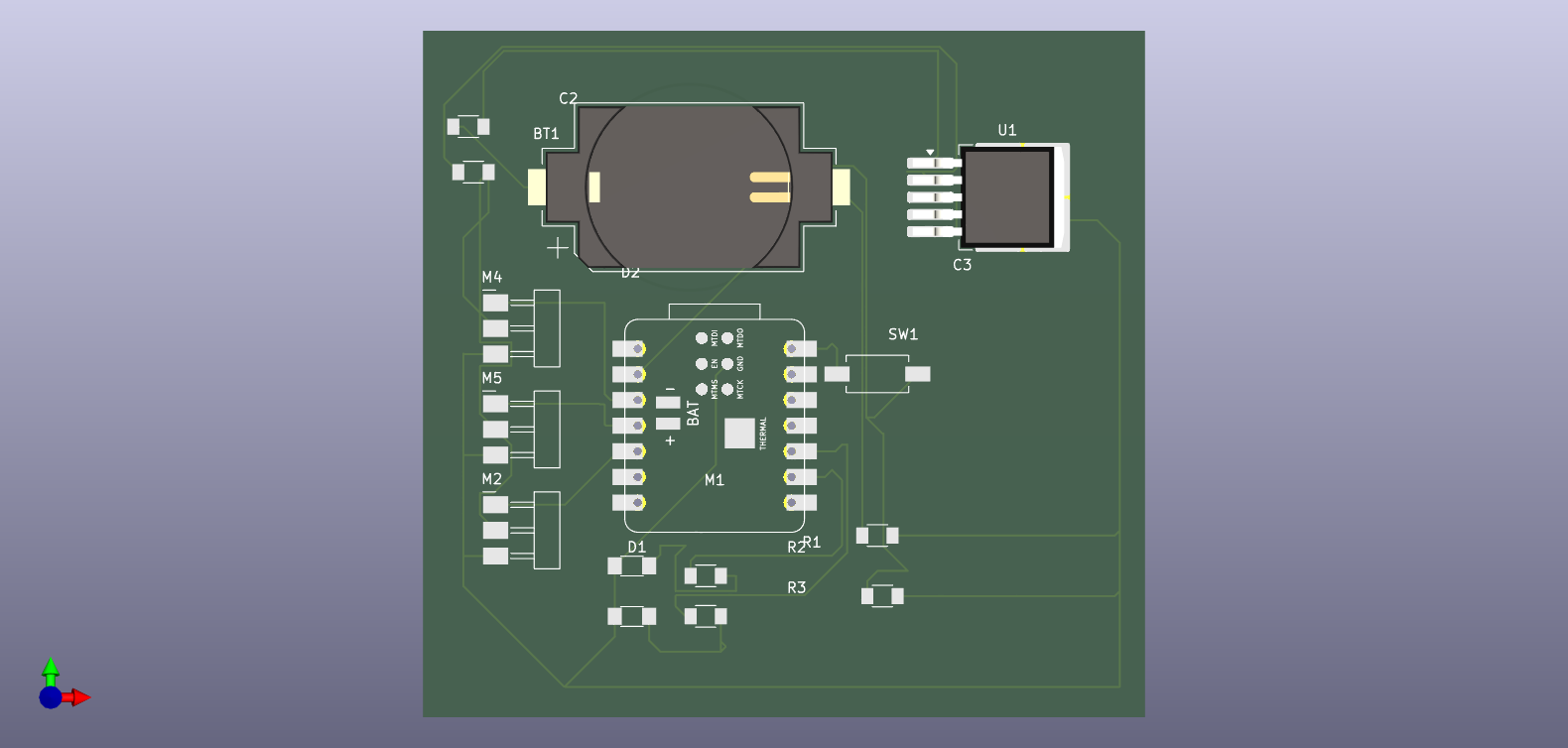
Once no errors are found, we can generate a 3D view of the PCB to visualize how it will look. The result should look like this:
Download Kicad Files
Conclusion
The PCB fabrication process was a valuable experience that allowed us to apply theoretical knowledge to real-world electronic design. We learned how to efficiently use KiCad to create schematics, assign footprints, arrange components, and route traces while ensuring proper electrical connections and design rules. Additionally, the Design Rule Check (DRC) helped us verify our work before generating manufacturing files.
This practice reinforced the importance of proper layout planning, trace organization, and error checking in PCB design. By visualizing the board in 3D, we gained a better understanding of component placement and manufacturing constraints. Moving forward, these skills will be essential for designing and fabricating more complex circuits efficiently.
