8. Electronics Production
This week, I made the PCB I designed for week 6 using the monoFab SRM-20 Desktop Milling Machine.
You can check the week assignment here.
Preparation
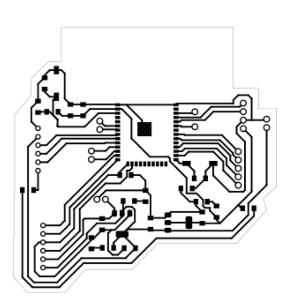
First, I printed my design to check that all the components fit.
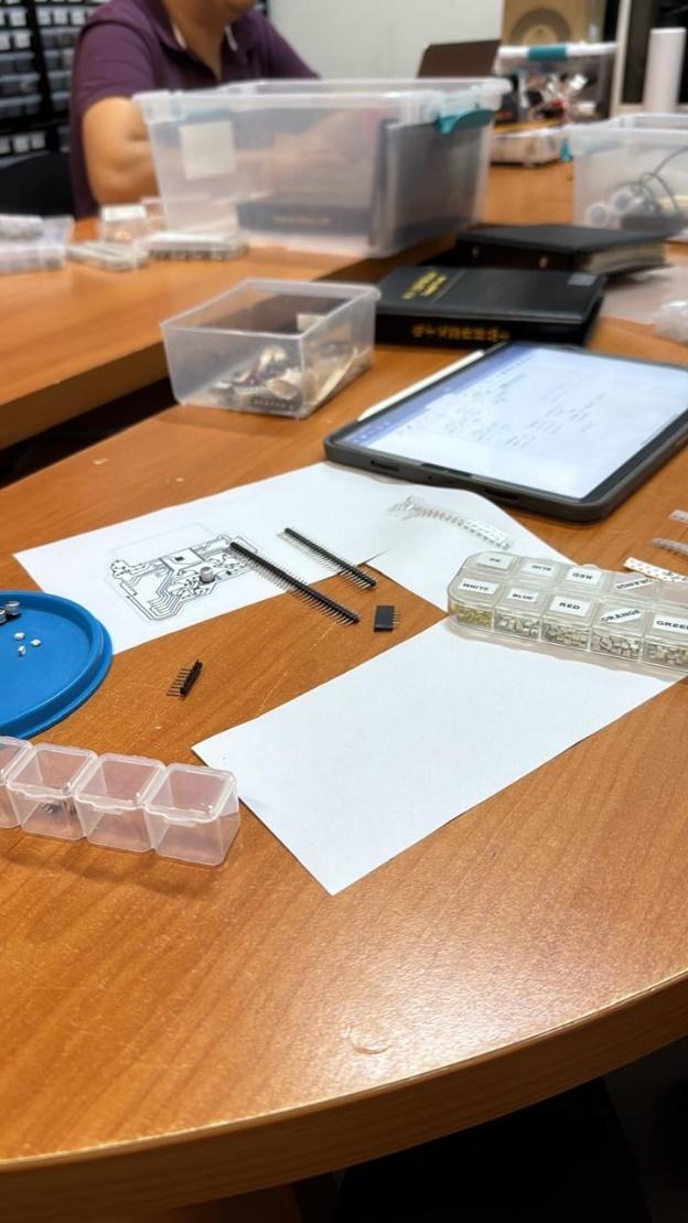
Then I gathered all the components I needed to solder.
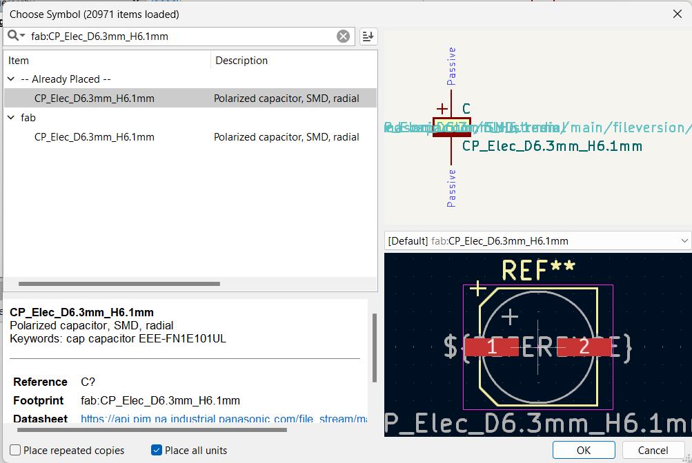
I realized that there weren't 22uF capacitors with the footprint I chose on KiCad, so I changed it to the available one.
Exporting and Configuring
I exported the different layers into SVG files and configured the paths on this webpage. I have the KiCad 8.0 version installed on my computer, so I didn't have any issues while exporting the SVG files.
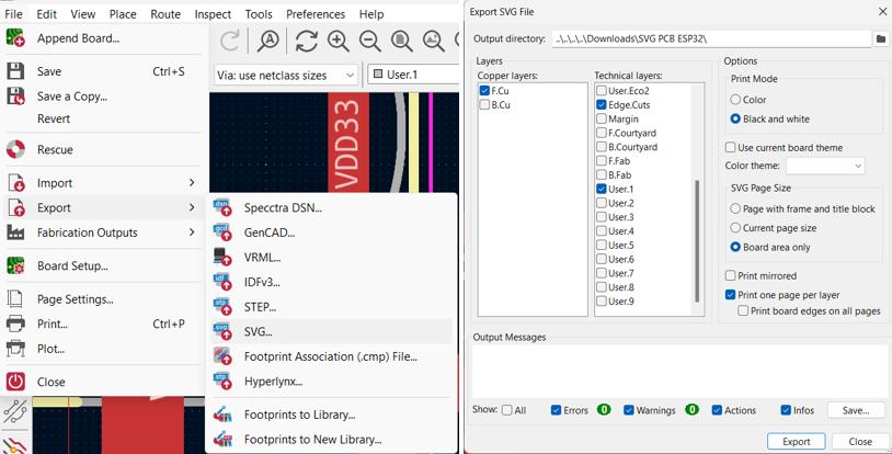
I only selected the layers I needed.
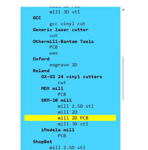
Once inside the page, I right-clicked to open the menu, then clicked on "programs," then on "open program" and then scrolled down until I found "mill 2d PCB" for SRM-20.
The configuration interface appeared.
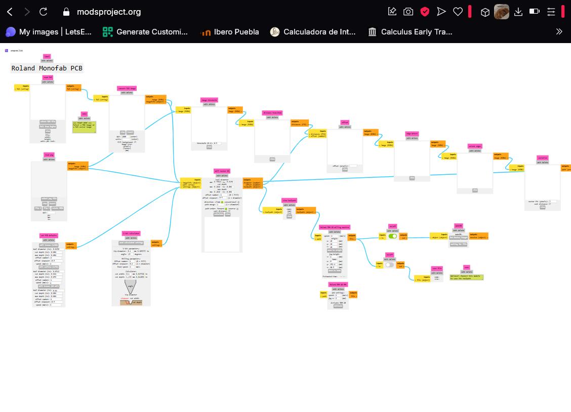
The parameters I changed were the feed rate, tool diameter, milling operation, and offset number depending on the layer I selected. I also set the origin to 0,0,0.
Milling the PCB
I stuck the copper plate to an MDF bed with double-sided tape.
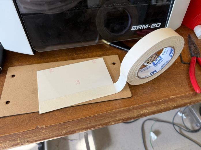
Then I screwed the bed into the monoFab.
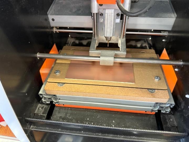
I connected my laptop to the monoFab and used the VPanel for SRM-20 to set the origin for the x and y axis.
You can download VPanel here, and the driver here.
Here's the VPanel interface:
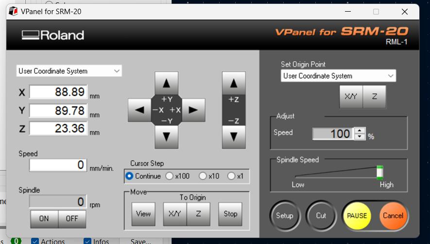
You can move the machine's nozzle by clicking the arrows and selecting the Step; the x100 will move the nozzle 1mm, the x10 will move the nozzle 0.1mm, and the x1 will move the nozzle 0.01mm.
To set the origin, I moved the nozzle to the desired position and then hit the "x/y" button on the top right side to save the coordinates. I had to set a new z-axis coordinate every time I changed the milling tool.
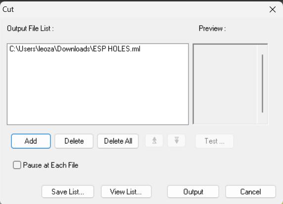
Once the origin was set, I clicked on "cut," which opened a new menu from which I selected the file.
On KiCad, I made circles for each pin I will be using.
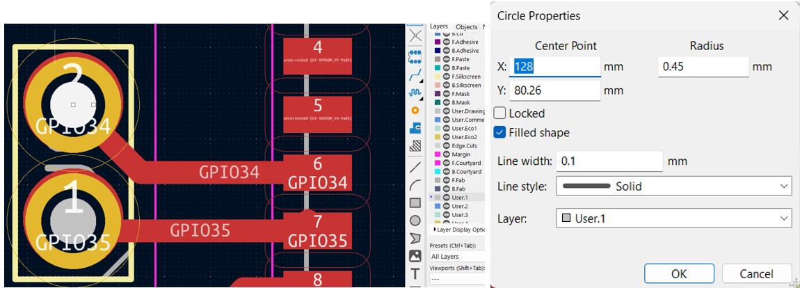
I used the layer named User.1, the holes have a 0.45 mm radius (you can change the circle's properties by selecting it and pressing the "e" key).
To configure the paths on the webpage, I selected "mill outline" and changed the tool diameter to 0.5mm, the offset number to 2, and the speed to 0.8 mm/s.
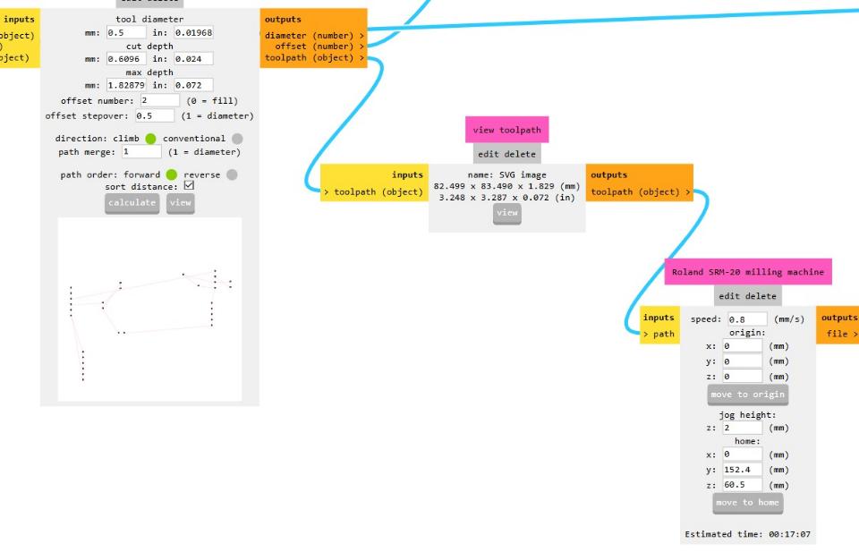
Once I had all the parameters set, I clicked on "calculate" and then "view" to make sure the paths were calculated correctly. To download the new file, I clicked on the following button and then recalculated the paths.
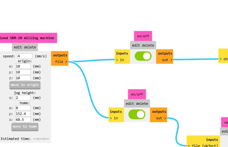
I put the 0.5mm mill into the nozzle and calibrated the z-axis origin by hitting the "on" button on VPanel and slowly moved the nozzle downwards until I saw small copper chips. I saved the origin and then selected the file to cut.
Issues
I first used the 0.8mm mill tool with a speed of 2mm/s, but I mistakenly thought that I made the circles on KiCad with an 8mm diameter, but I had an 8mm radius. I realized my mistake after the machine finished milling the holes, so I had to start over.
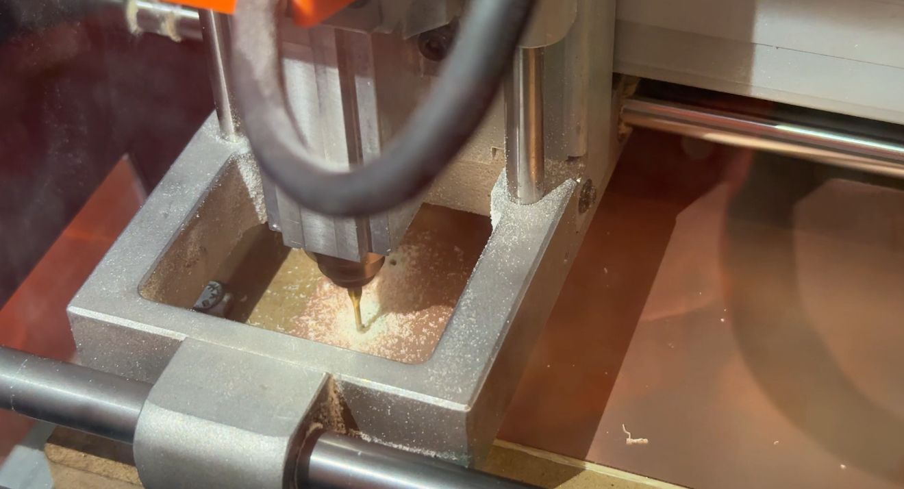
This time, the monoFab where I made my first attempt was busy, so I used the second one available at my fab. However, the tool didn't fully enter the nozzle, so after making the first hole, when it moved to make the second hole, the tool slipped. Due to the nozzle movement, it got stuck, and I broke. That's why I ended up using the 0.5mm tool.
To configure the paths on the webpage, I imported the F.Cu layer as SVG. I selected "mill traces", inverted the image, and changed the offset number to 2, I left the other settings to default.
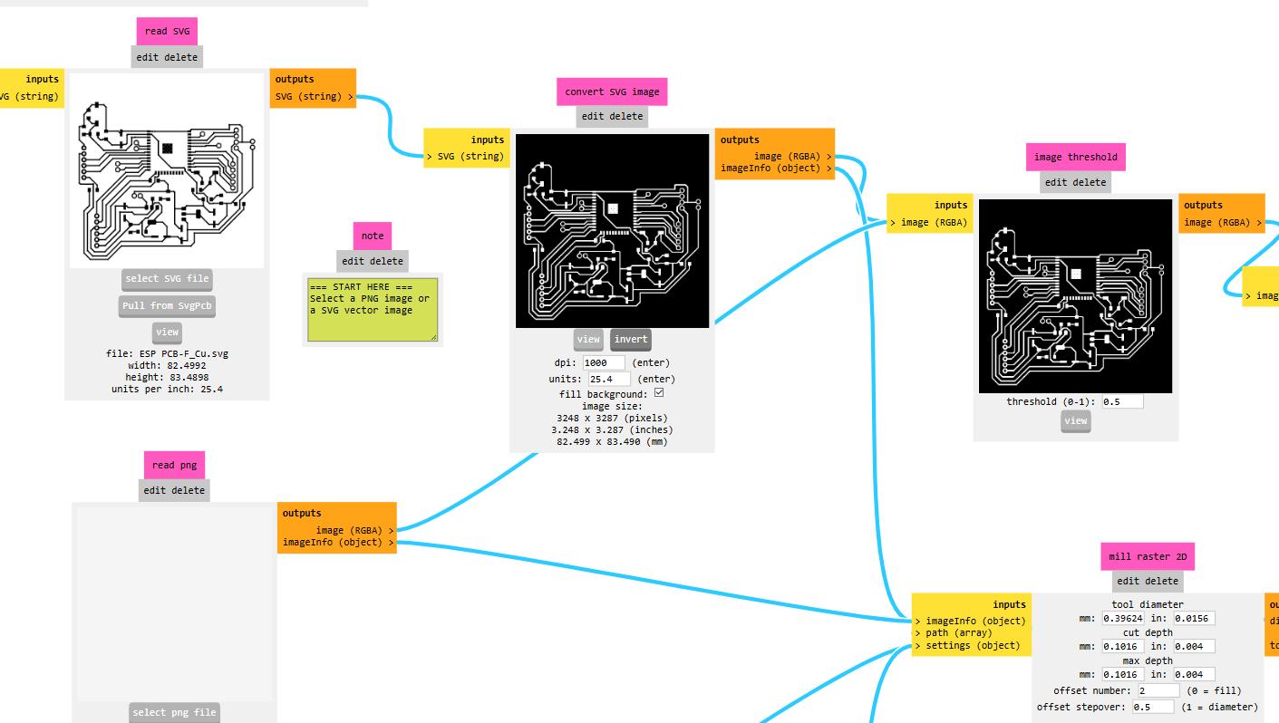
Once I had all the parameters set, I clicked on "calculate" and then "view" to make sure the paths were calculated correctly. To download the new file, I clicked on the following button and then recalculated the paths.
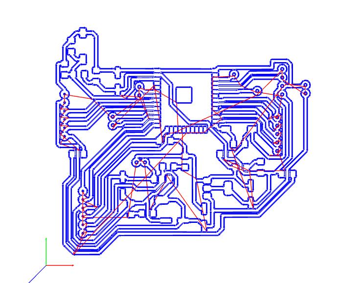
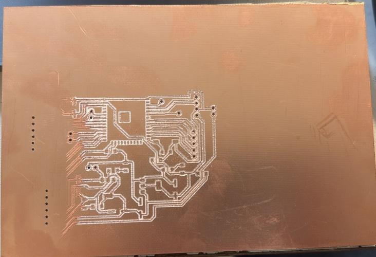
I used a V-shaped engraving tool, calibrated the z-axis origin by hitting the "on" button on VPanel, and slowly moved the nozzle downwards until I saw small copper chips. I saved the origin and then selected the file to cut.
The first time, I didn't see that some parts of my design weren't going to be cut, and due to the monoFab's bed inclination, the tool broke because on one side it cut deeper.
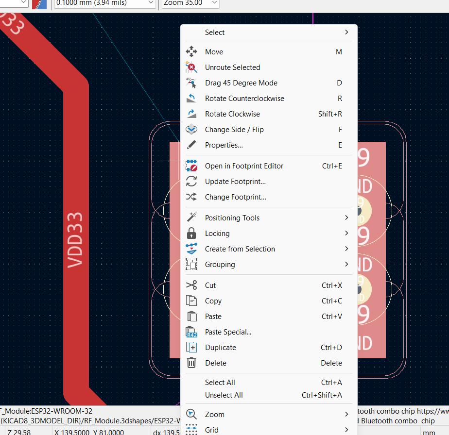
I modified the ESP32 WROOM-32 footprint on KiCad to have a 0.4mm separation between each pin. To do so, I right-clicked on the footprint inside the PCB editor and changed the rectangle sizes.
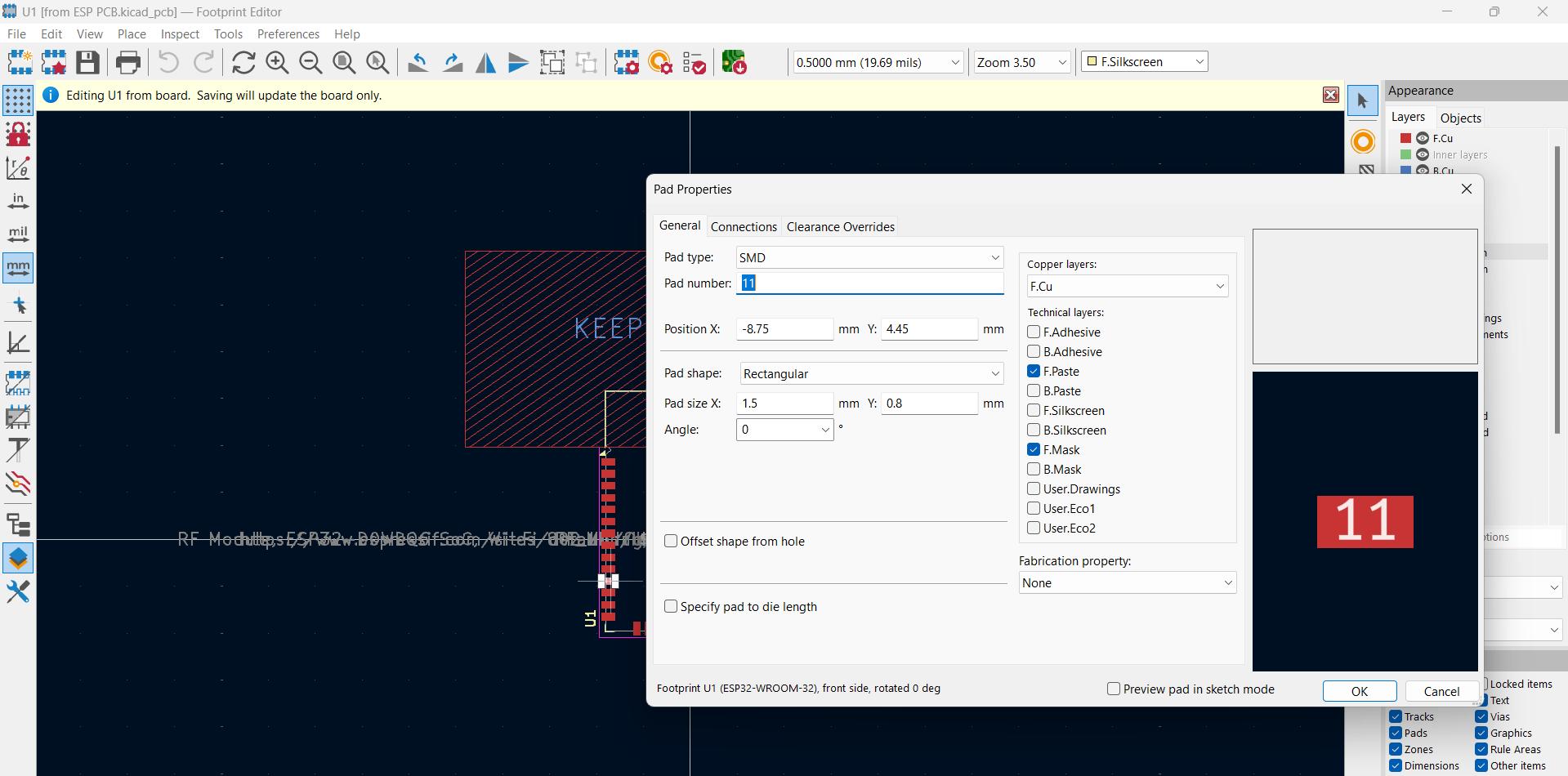
I also added some circles to this layer, so the pin holes had enough copper surrounding them to solder the pins.
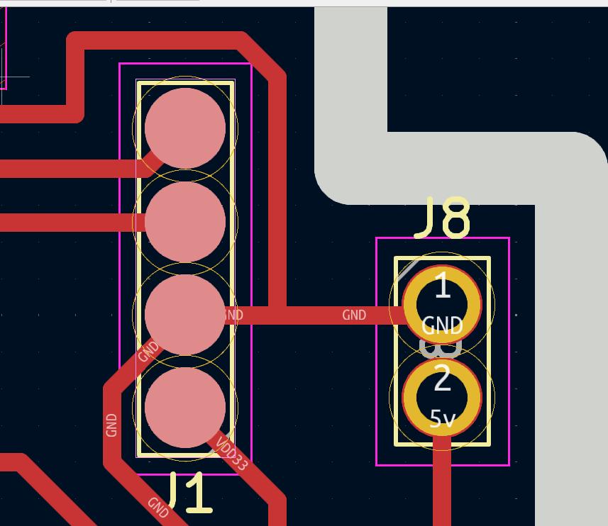
The circles have a 1mm radius.
I exported the layer again and configured the paths on the webpage, I had to start over my PCB by milling the holes and then the tracks with a new tool.
Since I broke the 0.8mm milling tool, I had to use the 2mm tool, so I had to change my PCB's outline on KiCad to make sure there was enough space between the edge and the tracks.
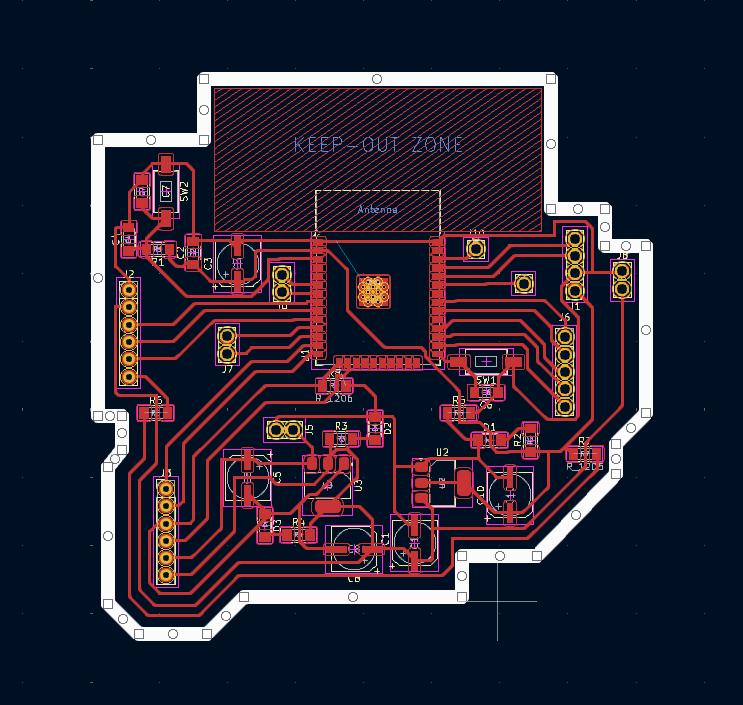
To configure the paths on the webpage, I imported the Edge Cuts layer as SVG. I selected "mill outline" and changed the tool diameter to 2mm, I left the other settings to default.
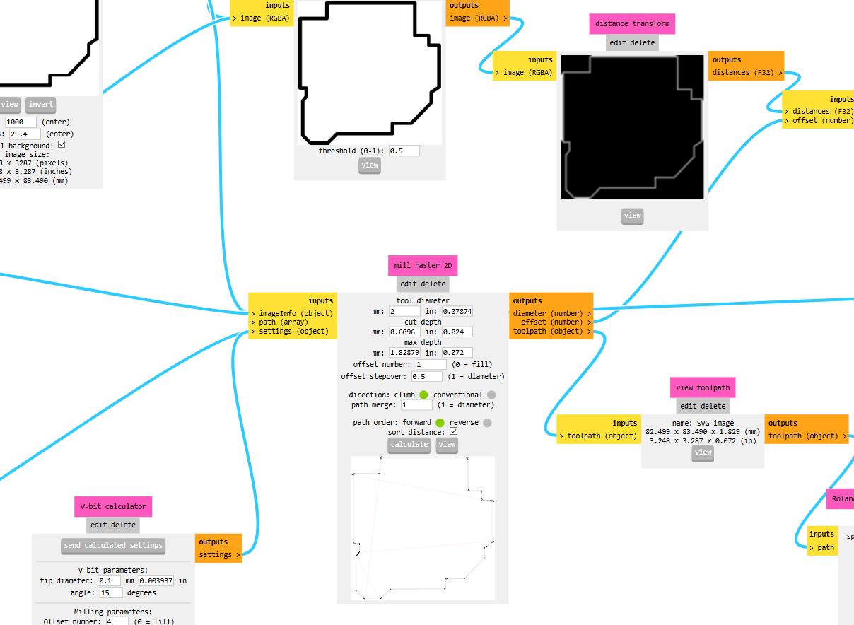
I set the new origin for the z-axis and started milling the outline:
Here's the result:
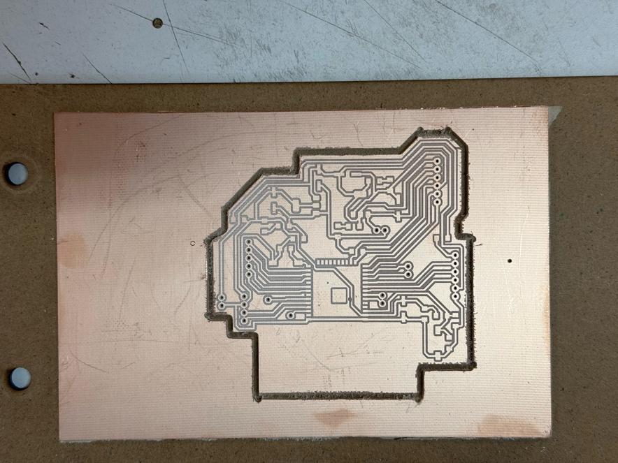
Soldering and Programming
I cleaned the PCB after each layer with a vacuum cleaner.
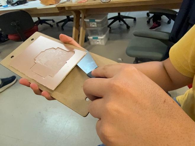
I removed the copper plate from the MDF bed with a spatula and the double-sided tape.
Then I started soldering all the components into my PCB:
Here's the result:
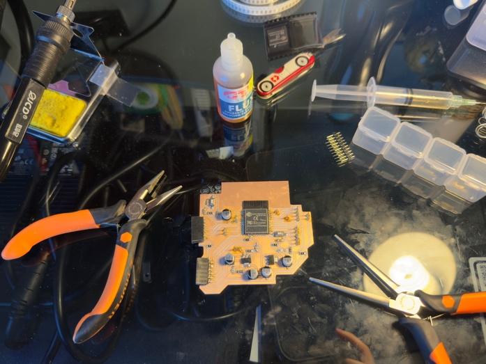
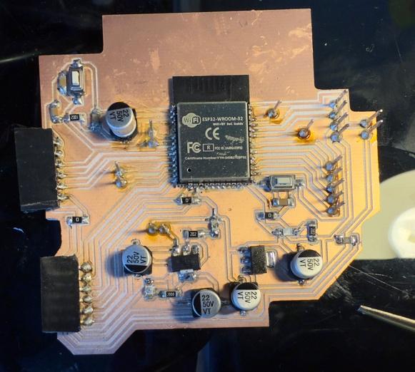
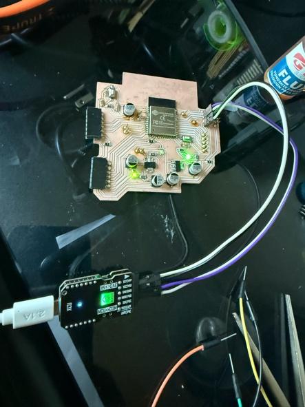
Then I had to program the ESP32, so I used a PIC/AVR UART XCU programmer and moved its switches to 3.3v and COM, I connected the pins I left on my PCB for this purpose:
I had some trouble uploading a code into my ESP32, but after pasting the error message from the Arduino IDE into DeepSeek, it told me how to use the EN and BOOT buttons to put my ESP32 into flashing mode and that I had to change the upload speed to 115200.
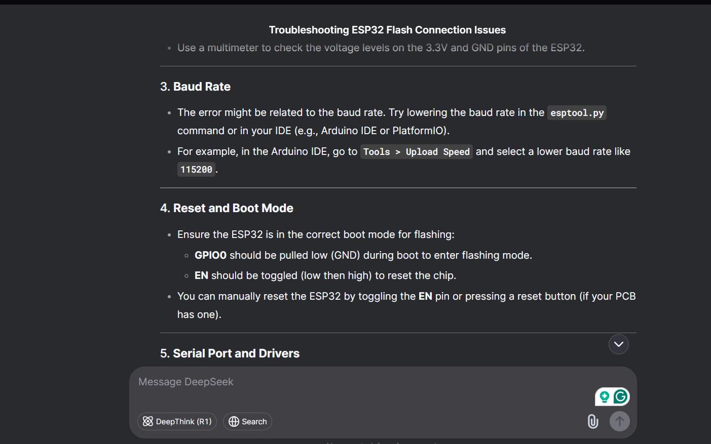
Here's the prompt I used:
I'm having some troubles programming an esp32 wroom 32 to which I made a custom PCB: Sketch uses 286273 bytes (21%) of program storage space. Maximum is 1310720 bytes. Global variables use 20392 bytes (6%) of dynamic memory, leaving 307288 bytes for local variables. Maximum is 327680 bytes. esptool.py v4.6 Serial port COM12 Connecting.... Chip is ESP32-D0WD-V3 (revision v3.1) Features: WiFi, BT, Dual Core, 240MHz, VRef calibration in efuse, Coding Scheme None Crystal is 40MHz MAC: 3c:8a:1f:09:e7:8c Uploading stub... Running stub... Stub running... Changing baud rate to 921600 Changed. A fatal error occurred: Unable to verify flash chip connection (Packet content transfer stopped (received 4 bytes)).
To change the upload speed, I clicked on "Tools" > "Upload Speed" and selected a baud rate of 115200. To enter flashing mode, I pressed and held the BOOT button and then pressed and released the EN button, I released the BOOT button until the code started uploading. To run the code, I pressed and released the EN button.
Here's the code I uploaded to my ESP32:
#include ESP32Servo.h
// Define the GPIO pin connected to the servo signal wire
const int servoPin = 13;
// Create a Servo object
Servo myServo;
void setup() {
	// Attach the servo to the specified pin
	myServo.attach(servoPin);
}
void loop() {
	// Move the servo from 0 to 180 degrees
	for (int pos = 0; pos <= 180; pos += 1) {
	myServo.write(pos); // Set the servo position
	delay(15); // Wait for the servo to reach the position
	}
	// Move the servo from 180 to 0 degrees
	for (int pos = 180; pos >= 0; pos -= 1) {
	myServo.write(pos); // Set the servo position
	delay(15); // Wait for the servo to reach the position
	}
}
After uploading the code into the ESP32 I used my programer to power the PCB, I changed the switch to 5 volts.
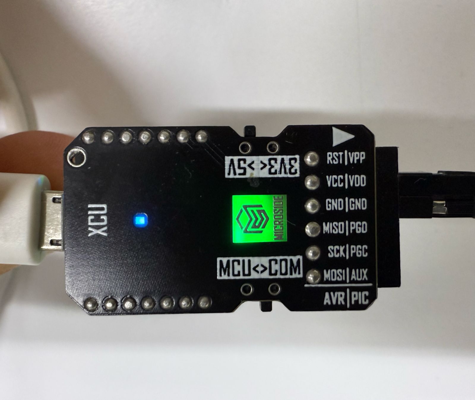
Here's the working program:
Summary
This week, I successfully milled, soldered, and programmed my custom PCB. I encountered some issues with the milling process, but I was able to resolve them by adjusting the tool size and reconfiguring the design. The soldering process went smoothly, and I programed the ESP32 after troubleshooting the upload speed and flashing mode.
