6. Electronics design
PCB stands for Printed Circuit Board. It is a board that has tracks that connect various points together, usually to connect components to build a circuit. For this week's assignment, I designed a PCB to use an ESP32-wroom32 for my final project, so I left the necessary connections for the drivers I will be using to move some motors.We also did a group assignment for this week you can find it here.
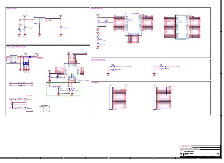
I started by doing some research about the necessary components I needed to use the ESP32-wroom32 and I found the manufacture´s schematic.
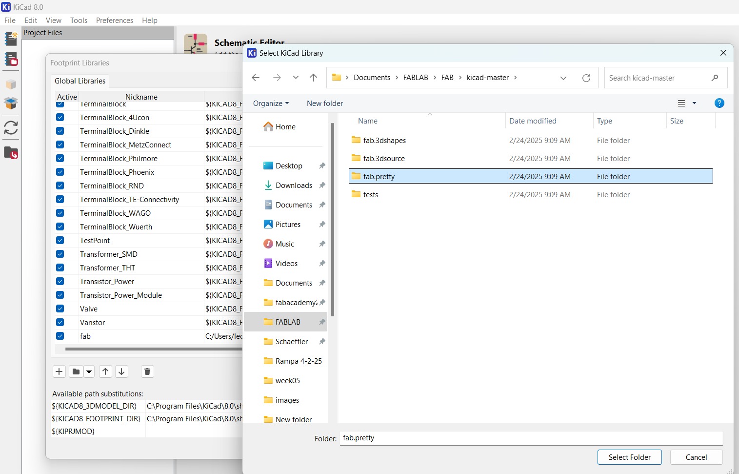
I designed the PCB using KiCad. I started by adding the necessary libraries. I´ll be using this folder provided by my local instructor.
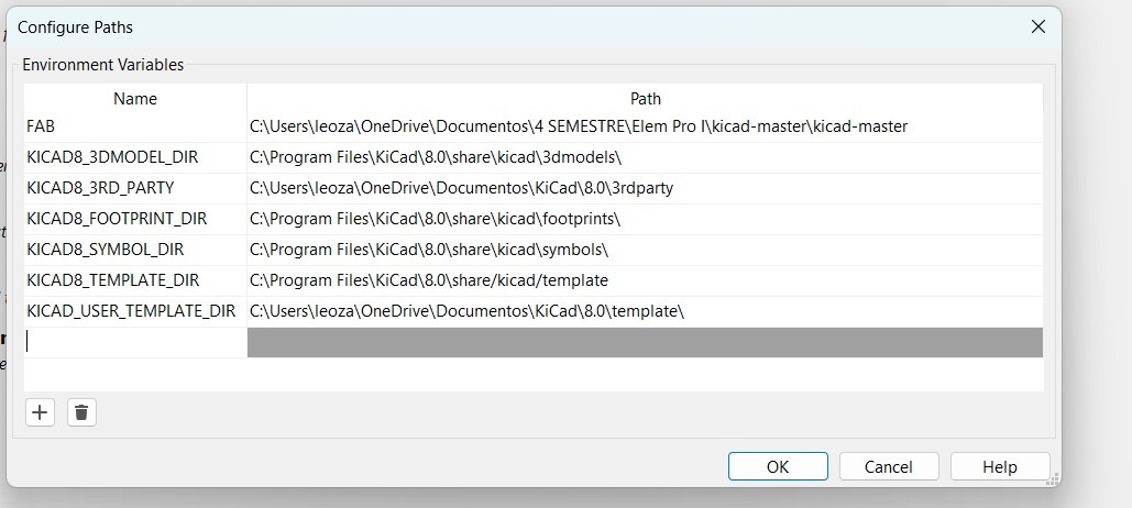
First click on "Preferences" and "Configure Paths", to add the folder hit the plus button and select the folder (If you move the folder to a different location you´ll need to update the path).
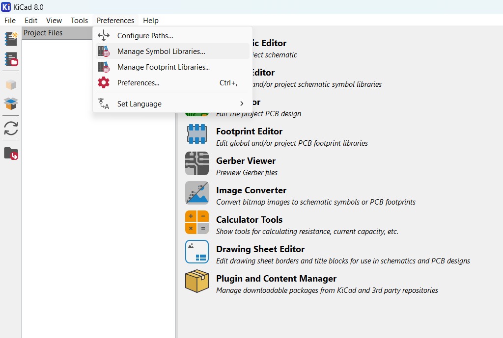
Then click on "Preferences" and "Manage Symbol Libraries"
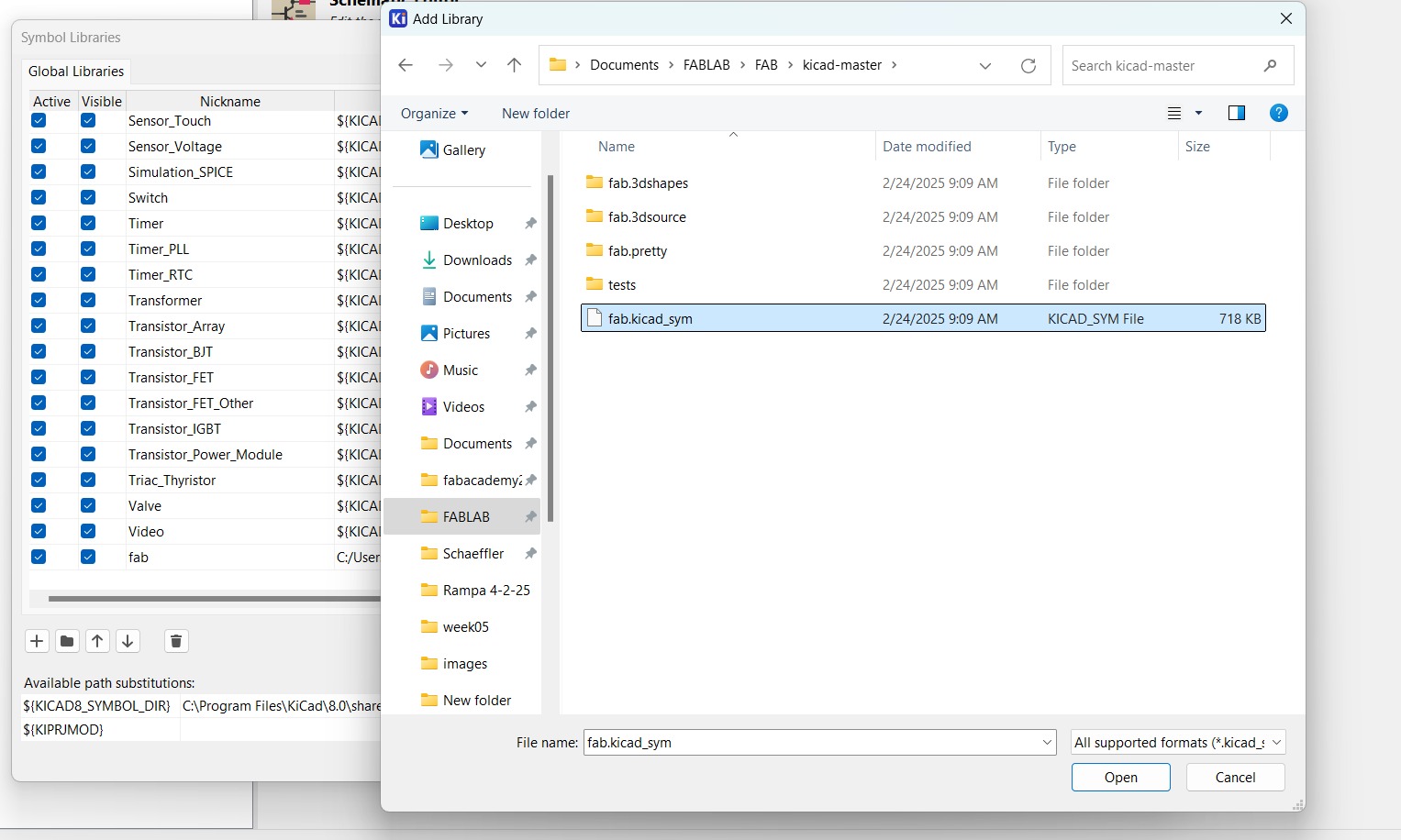
A new window will appear, add a nickname to the library and browse inside the folder until you find this file:
Do the same steps for "Manage Footprint Libraries" but select the following folder:
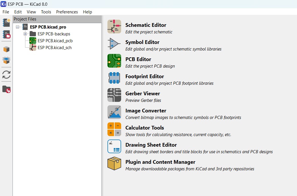
Now you can start designing your PCB. Click on "Create a new project" and name it. Once it´s created you will see the two files, the Schematic is the first file to edit since it´s where all the components will be added, the PCB file is where we make´ll all the final connections.
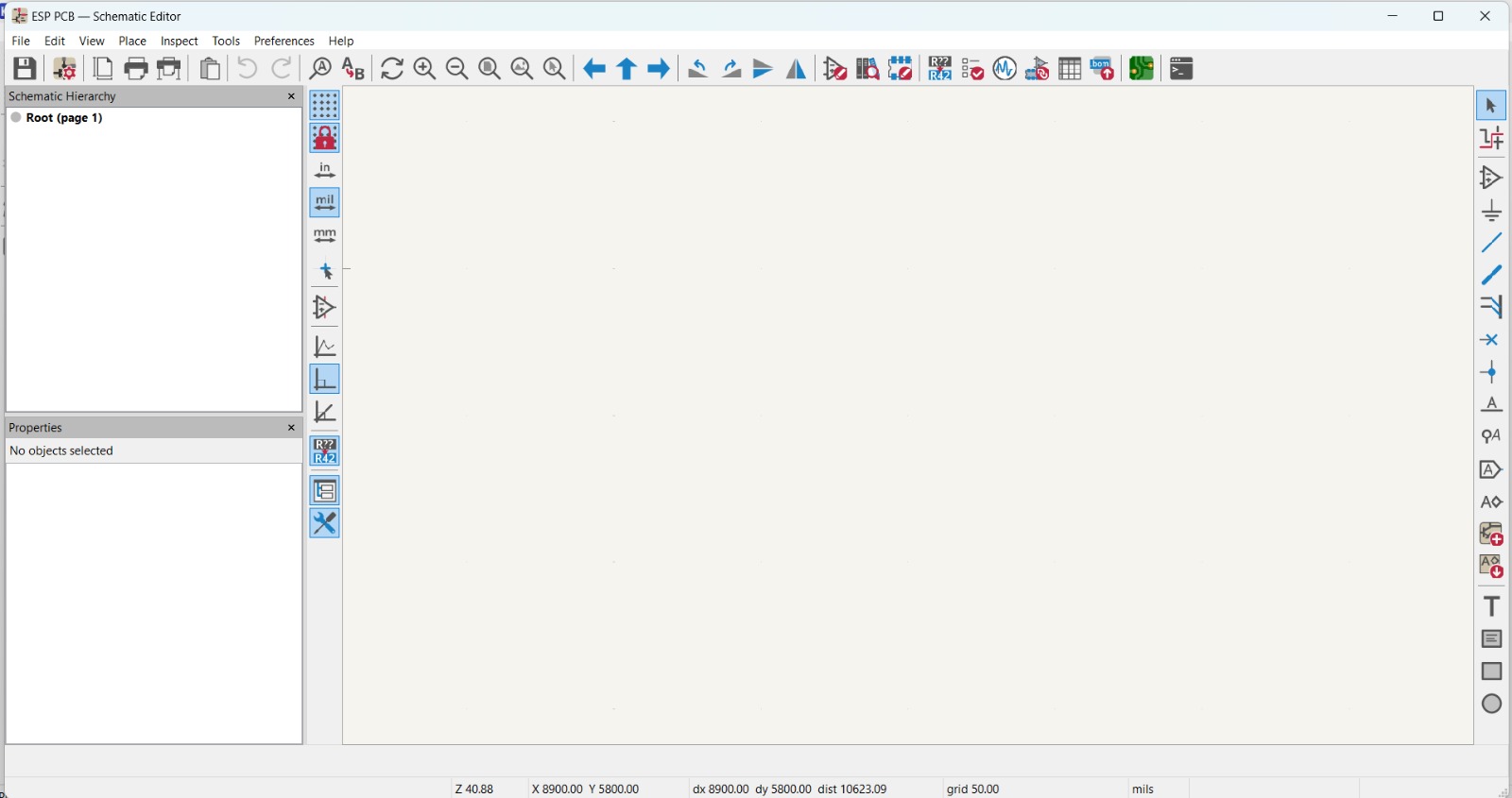
Here is the Schematic editor interface:
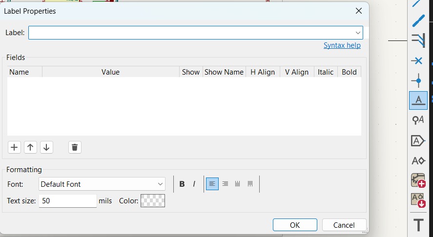
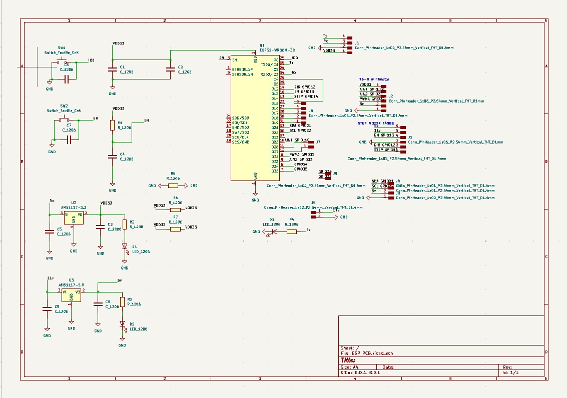
Click on the "Place symbol" button (third symbol on the right) and start adding the components. You can search for the components by name. You can rotate the component pressing the "R". You can wire the components to create a relation between them or you can use labels to connect them.
Like this:
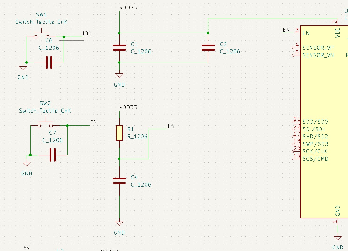
Note that I used labels to ovoid wiring all the grounds together and make the schematic design more organized.
On the manufacturer´s schematic there is a part showing how to connect a usb port and a USB to UART converter which you can add to program the ESP32, but I´ll be using an external converter, so I left the RX, TX, GND and VCC pins available to connect the converter.
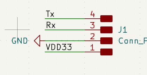
I also left some pins together to connect a TB6612FNG motor driver a A4988 driver and the I2C pins.
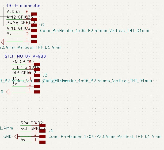
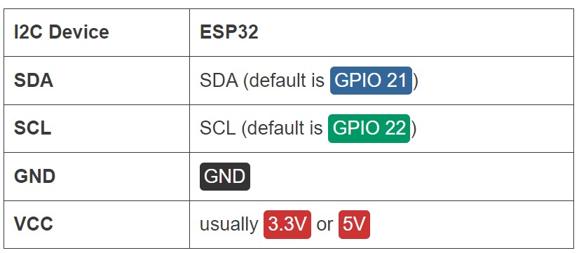
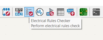
Once you have all the components added, you can use the Electrical Rules Checker to see if there are some mistakes made.
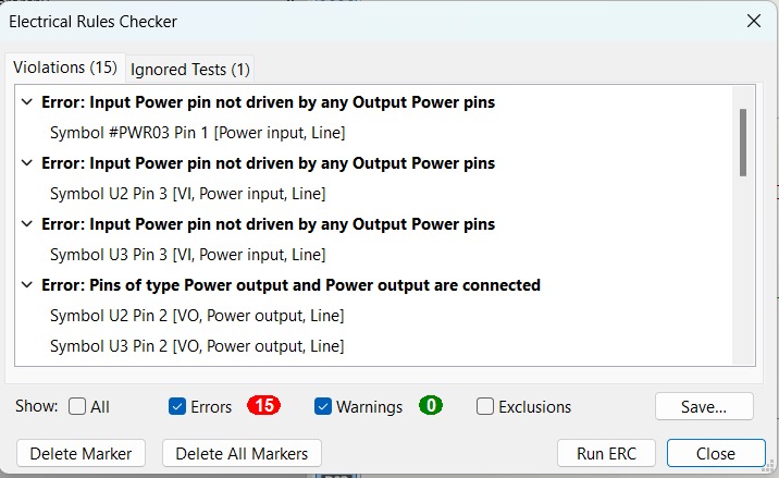
Once you run the checker a window will pop up displaying all the errors and warning, make sure there are no warnings. Some errors might appear, most of the time it´s because some pins are not connected, but read them to see if there is anything wrong.
I left some pins available just in case a need more, or if I decide to use this PCB for a different purpose.
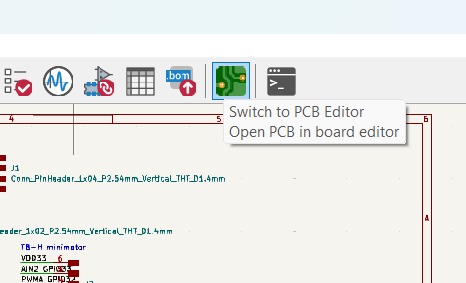
After making sure everything is fine click on PCB editor
Here is the PCB editor interface:
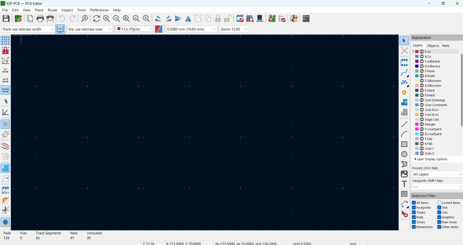
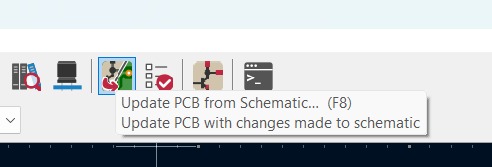
Click on "Update PCB from Schematic" to update the PCB with the components added on the schematic.
You will see that all the components will appear:
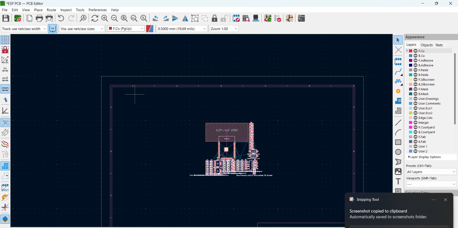
You can move each component separately and rotate them pressing "R".
Before connecting the components together I used the "Calculator tools" to calculate the track width since the motors I´ll be using will need a lot more current than the other parts.
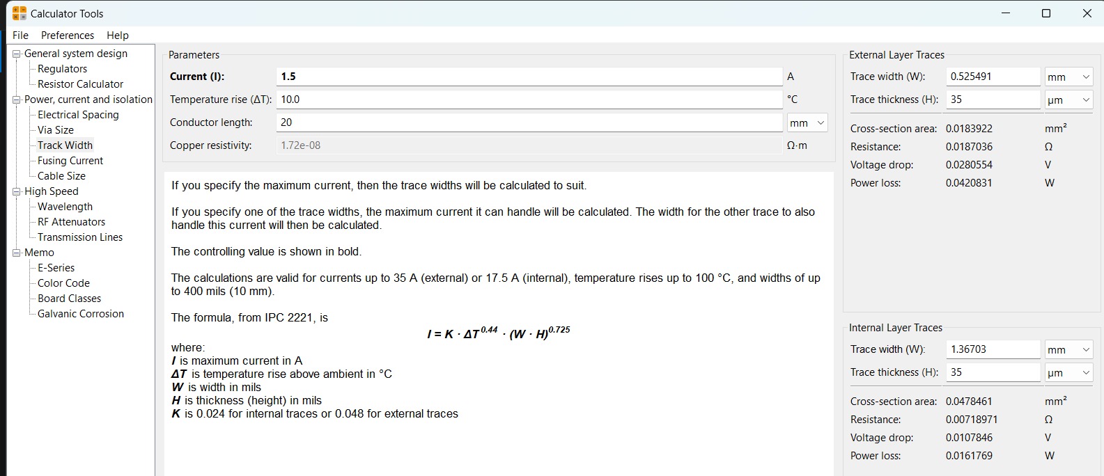
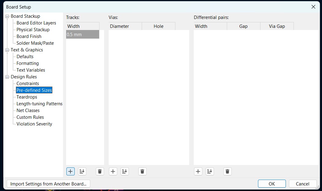
I only changed the current value to 1.5 Amperes, just to be sure. For these amount of current I need to have a track width of 0.5mm.
To change the track width on the PCB editor click on "Track" and then on "Edit Pre-defined Sizes"
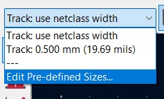
Click on "+" and add the new size.
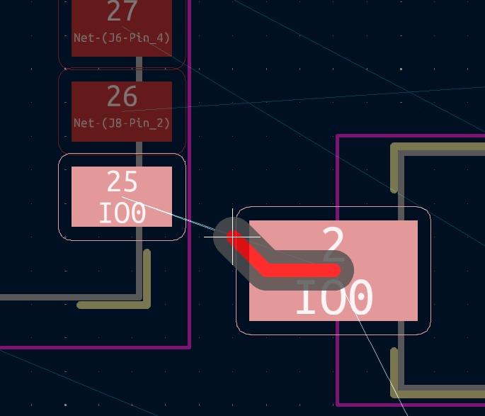
Once you saved the track width press the "X" key to start connecting the components:
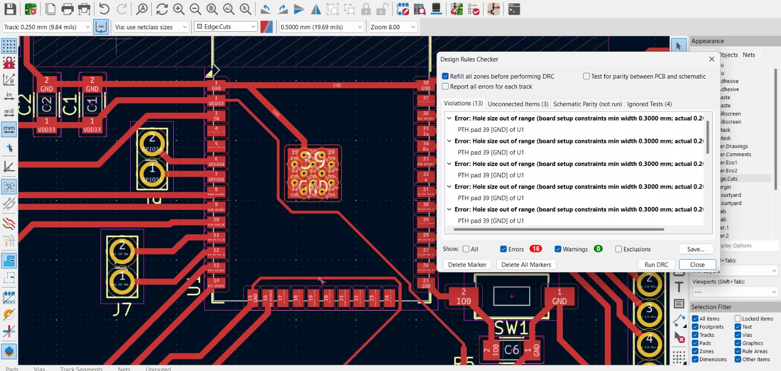
Make sure you have all the tracks connected by running the "Design Rules Checker".
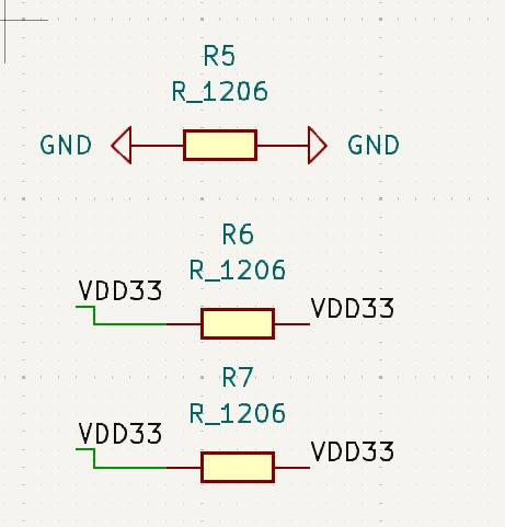
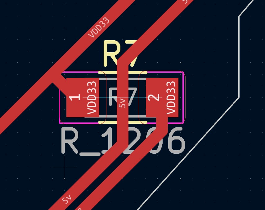
I had some troubles connecting everything together because some components got surrounded by other tracks so on the schematic I added some 0 value resistors to serve as "bridges"
Once you have all the tracks connected you can add the outline of the PCB. Click on "Add graphic line or polygon" and draw the shape of the PCB.
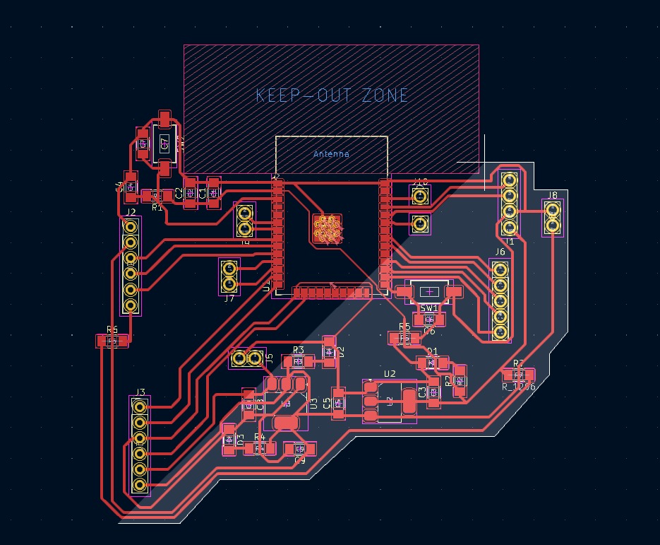
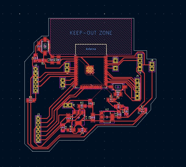
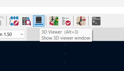
Once you have the outline you can click on "3D viewer" to see a preview of the board.
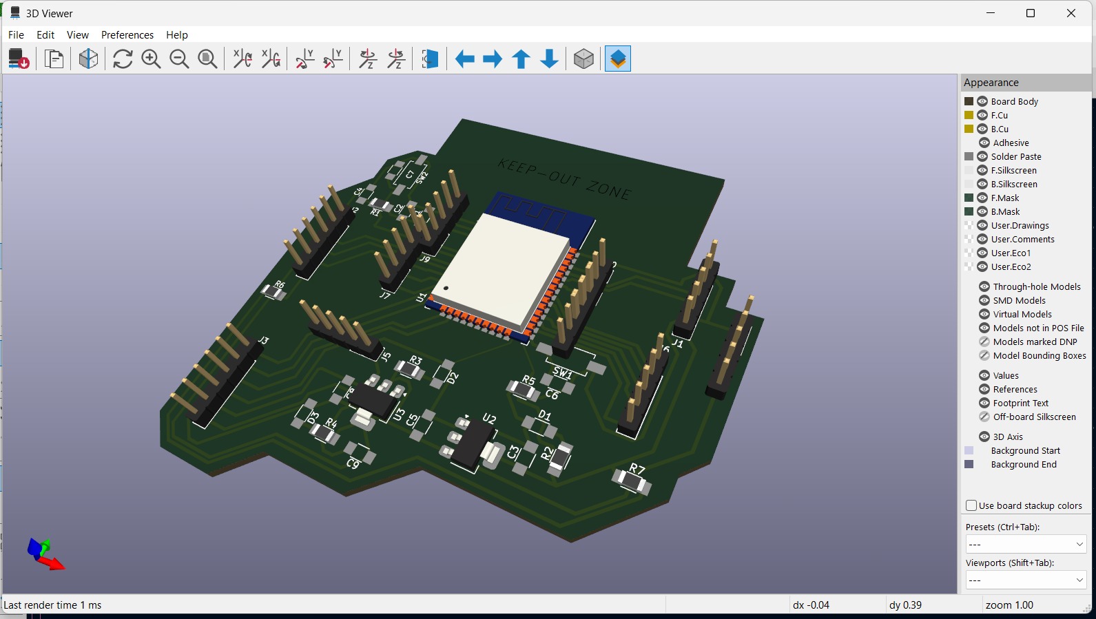
Here is the list of components I will be using to build this PCB:
- ESP32-wroom32
- 4x 0.1uF capacitor
- 5x 22uF capacitor
- 2x 2k resistor
- 1x 10K resistor
- 3x LED
- 4x 0 resistor
- x2 6x3.5mm button
- 10x female pin
- 21x male pin
- 1x AMSL117 3.3v regulator
- 1x AMSL117 5v regulator
I will be using these components since those are the ones that where indicated on the manufacturer´s schematic. I added a 5v regulator since I need 5v to power a small DC motor, I considered a 11v power source because I will use a stepper motor for my final project, so i left some pins with that voltage.
Summary
For this week's assignment, I was able to design a PCB for my final project, using KiCad, I used the "Calculator tools" to calculate the track width and I changed the track width and the Rules Checkers helped me to see if there were any errors. It was a little bit challenging to connect all the components together it took way longer than I expected and I had to made some changes to the schematic to make it easier, but I was able to do it.
