6. ELECTRONICS DESIGN
- This week we need to create a development board with an EDA tool, using components from the library, and these components should communicate with an integrated microcontroller. In my case, I used KiCAD and I will document the steps I used to complete the assignment.
- GRUPAL ASSIGNMENT -
- HOW TO SETUP KICAD? -
DOWNLOAD KICAD
To download KiCAD, we go to KiCad and download the lastest update
CLONE AND INSTALL FAB REPOSITORY
After downloading KiCAD, e need to install the FabLab library, so we can work with the electronics parts that we have available. First we download FabLab Library for KiCAD. To add the library to KiCAD, follow the instructions
- Clone or download this repository. You may rename the directory to fab
- Store it in a safe place such as ~/kicad/libraries or C:/kicad/libraries
- Run KiCad
- Go to "Preferences / Manage Symbol Libraries" and add fab.kicad_sym as symbol library
- Go to "Preferences / Manage Footprint Libraries" and add fab.pretty as footprint library
- SHEMATIC EDITOR -
After install out library, we can star designing uor electronic design. We create a new project: File / New Project
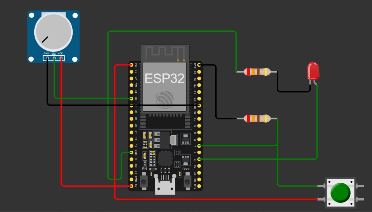
We will create the same simulation that I made in
To download KiCAD, we go to WEEK 4
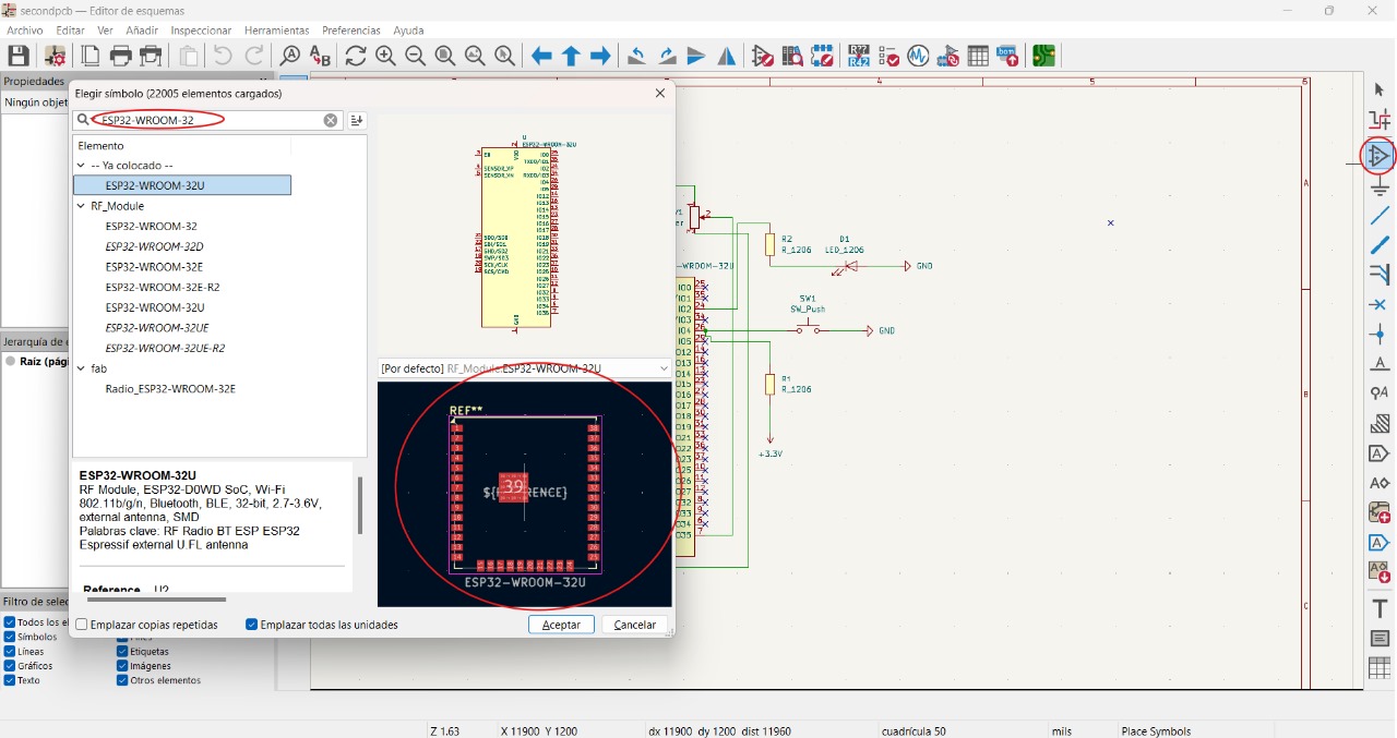
To add electronic designs to the template, select "place symbol" to place them. To ensure our designs are correct, they should have a drawing showing how they would look in the "board editor". I added the ESP32-WROOM-32U microcontroller first since it's the most similar to the ESP32-WROOM without being the complete microcontroller and only being the chip
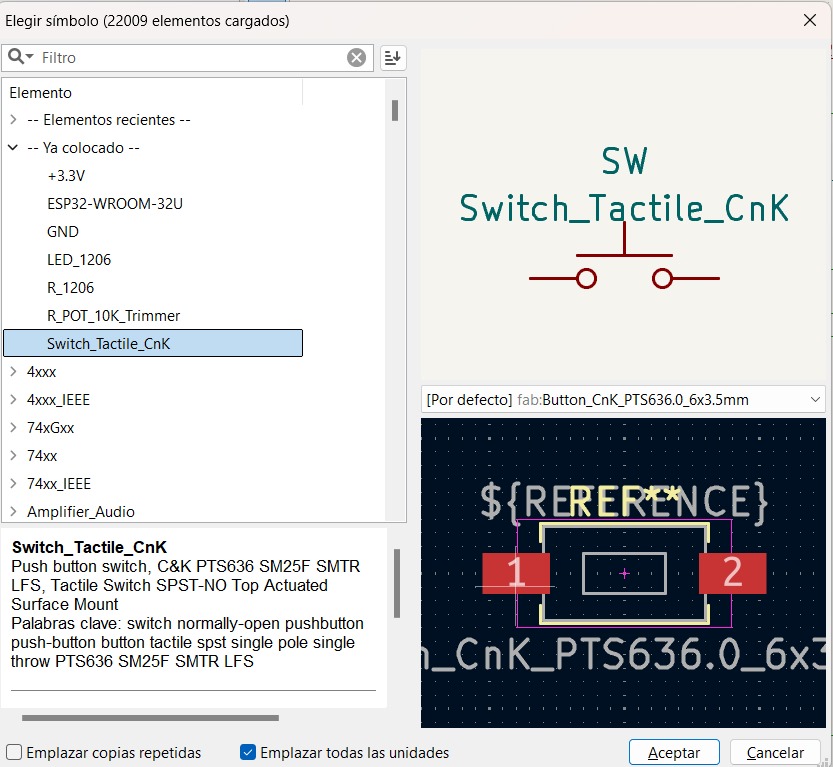
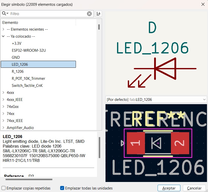
Using the same tool, we will add the following components to the template: LED_1206, R_Pot_10k_Trimmer and Switch_Tactile_CnK
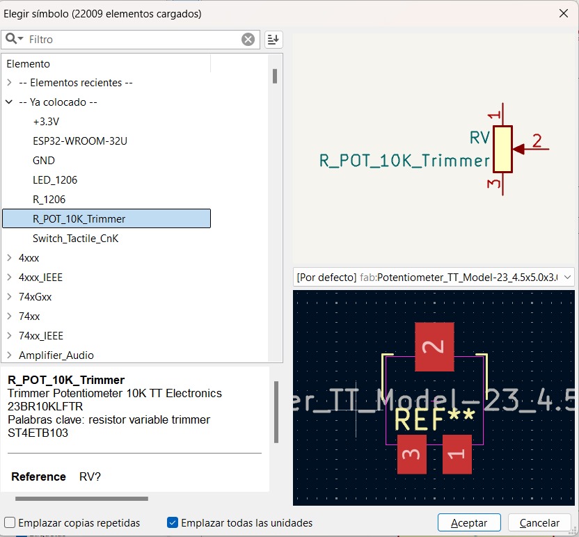

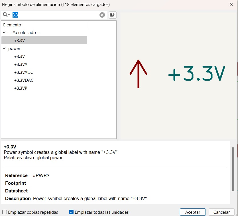
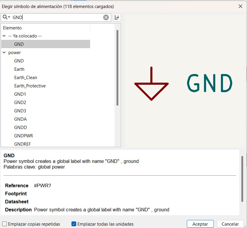
And finally, 2 resistors, 2 grounds, and 1 voltage
Using the "Draw wires" tool or with the letter W, we can connect all the components in the following way
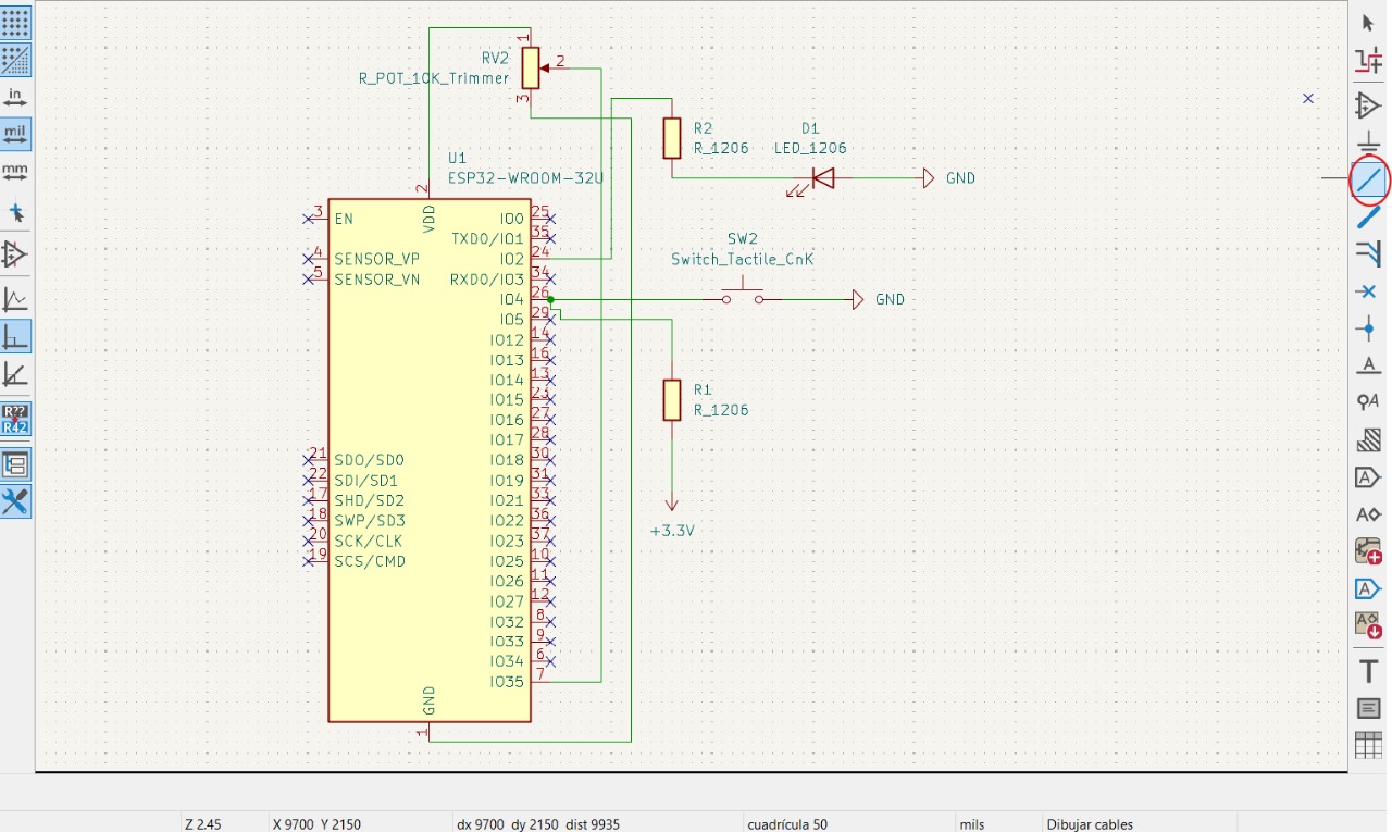
With the help of the "Draw wires" tool or with the letter W, we can connect all the components in the following manner. We'll make some changes within the schematic so that the cables aren't too long, making the schematic aesthetic and easy to read. We can give the same value to elements by giving them the same name using the "Place Net Labels" tool.
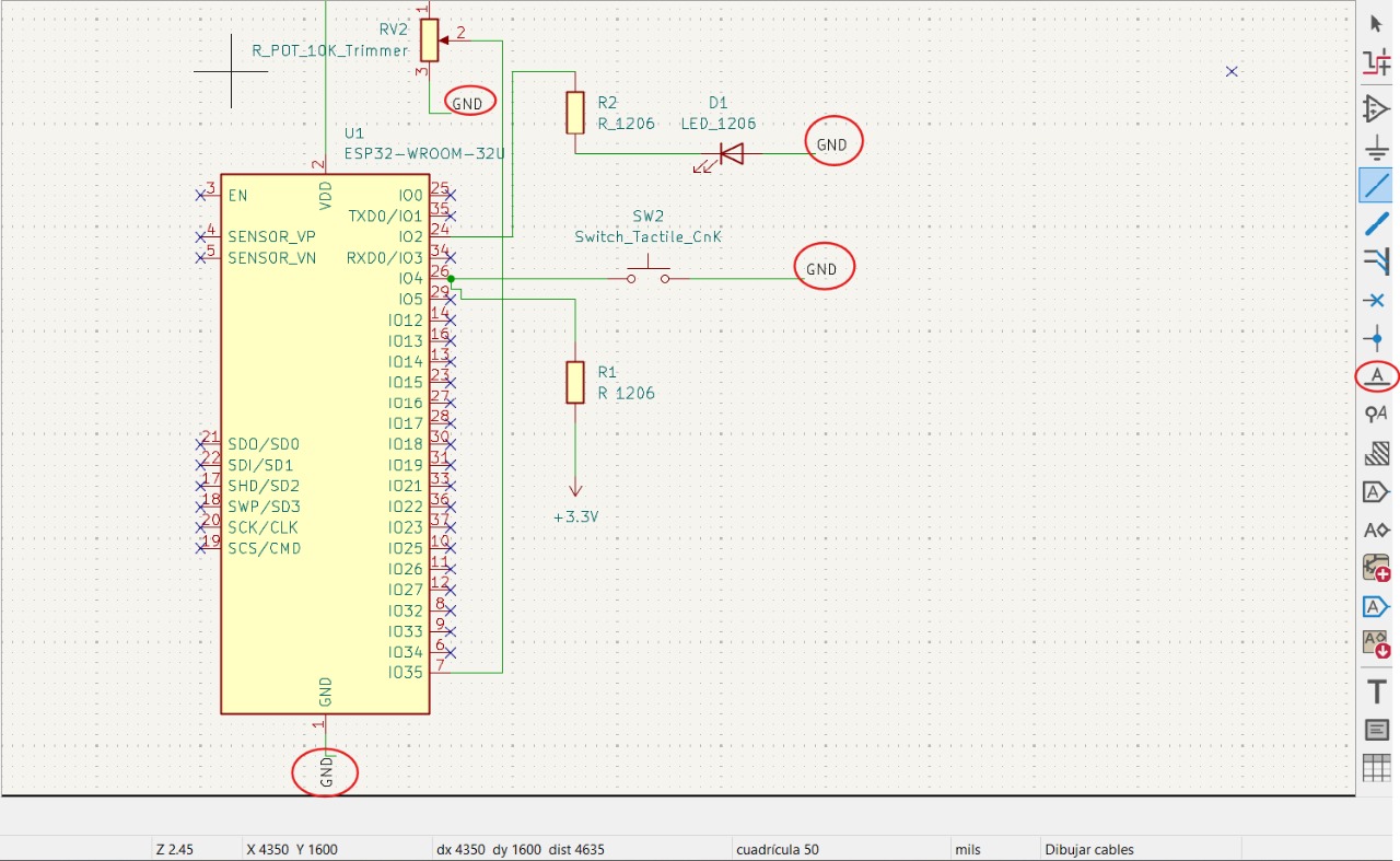
PLACE NO CONNECT FLAGS
In order to know if our board is complete and without any errors, follow "Inspect/ Electrical Rules Checker/ Run ERC".
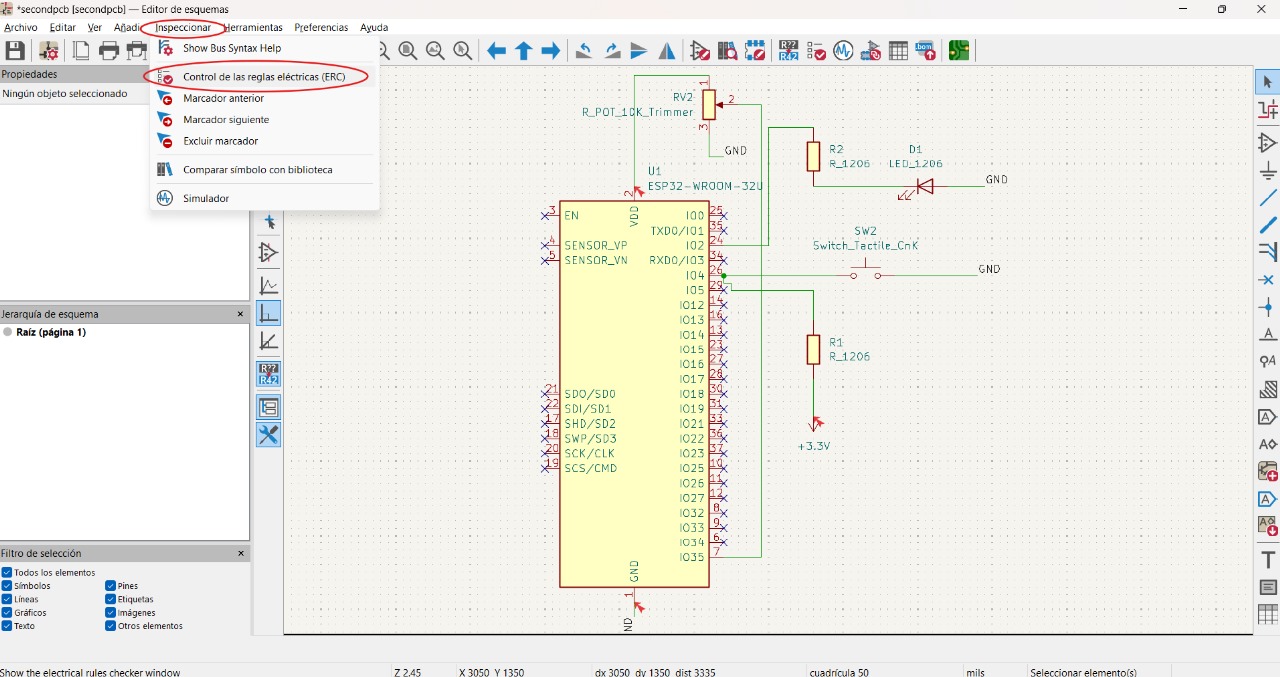
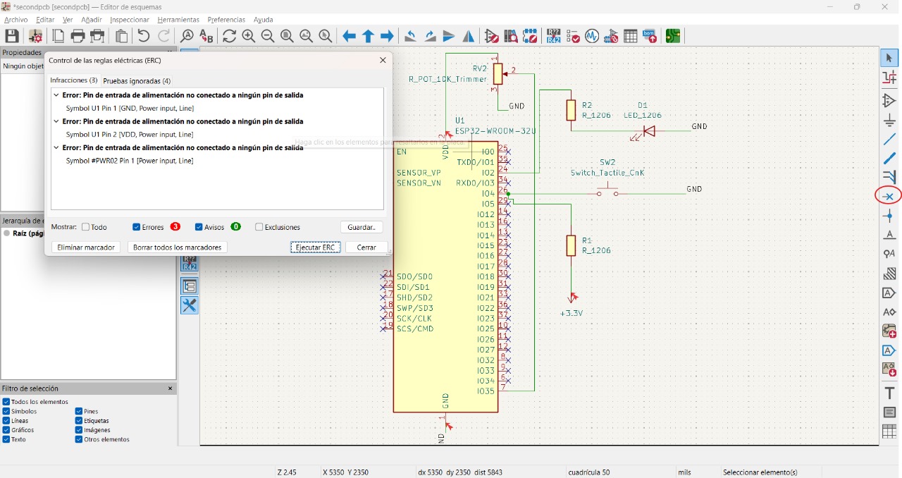
One of the errors that will appear is that the pins are not connected to anything, which isn't really an error but can be resolved with the "Place Not Connect Flags" tool
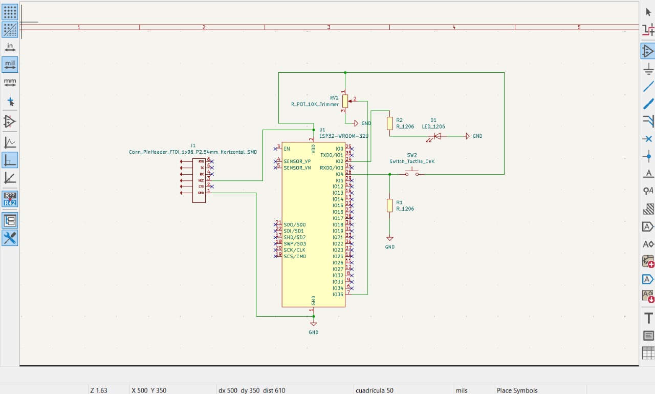
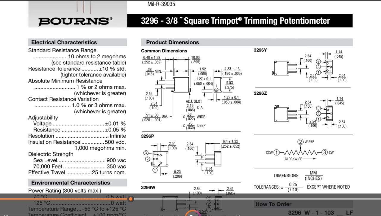
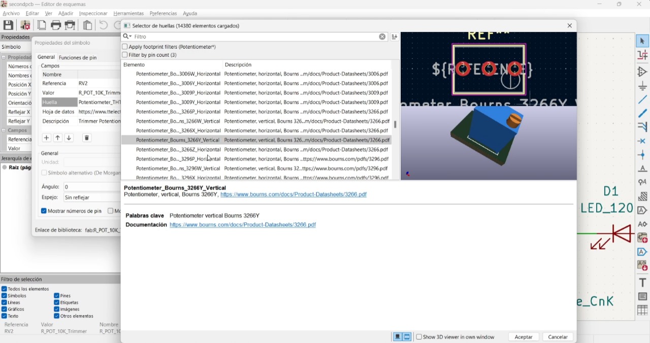
Before continuing, I began to notice certain errors that I had in the schematic. I was able to notice them thanks to an example from teacher Huber Giron Nieto, as he showed us an example and he was also using the same microcontroller as me. I will show some changes that I made to the schematic where I noted my errors.I noticed another error was that I had placed a potentiometer that wasn't available at the University, so I went to look for the one that was available and checked its datasheet to confirm it was the right one.I also removed some voltages from the previous schematic and likewise placed "Power Symbols" instead of just "Net Labels" that give them that name and function if you place them where the microcontroller provides those signals. In my case, since the schematic doesn't have many components and functions, it will be better with the changes I made. What we will add will be to program the board and run the program
- ADDING FAB CONNECTOR FTDI, FAB POTENTIOMETER AND POWER SYMBOLS -
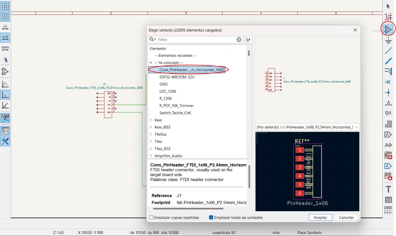
FAB CONNECTOR FTDI
When you find the device, you place it in this way
FAB POTENTIOMETER
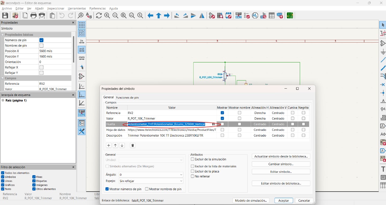
POWER SYMBOLS
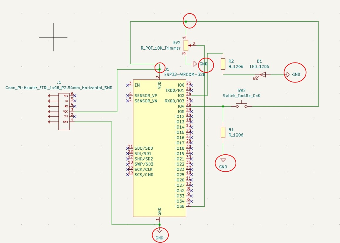
- CHANGE TO THE BOARD EDITOR -
The next step will be to use the "switch to board editor" tool

PLACING COMPONENTS AND CONNECTING
Using the "Route single track" tool, we can connect the cables this way, ad to be able to place them in a different way, we can rotate them with the letter "R"
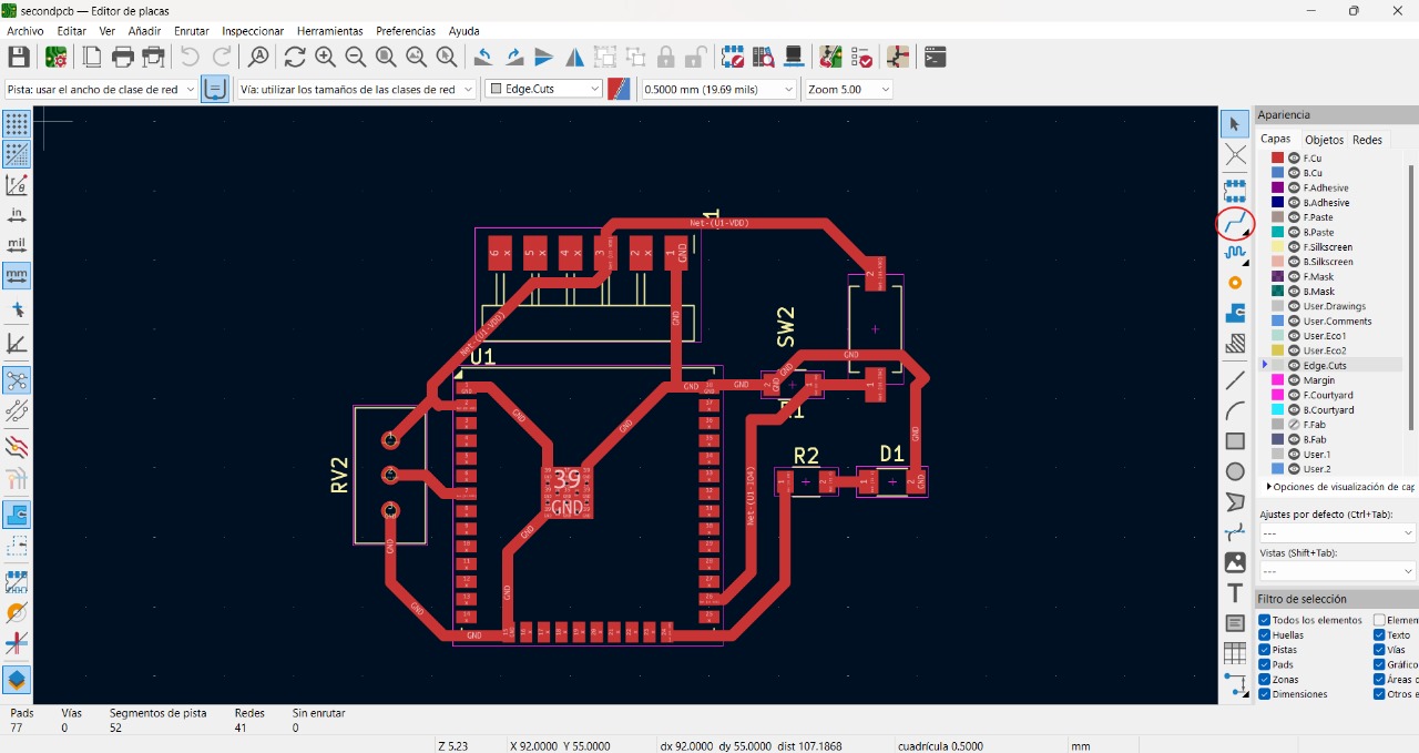
You can eliminate certain layers of the PCB where you can remove colored words using this bar and the eye icon

EDITING BOARD CONFIGURATION
If when connecting the cables some cannot connect between them, that will depend on the default settings that the application has set. We can change it in this way and in this case follow this configuration.
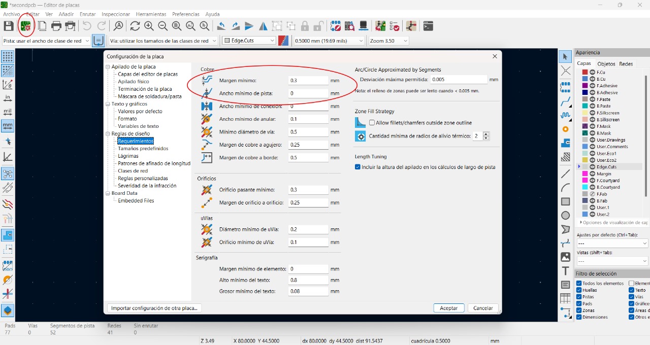
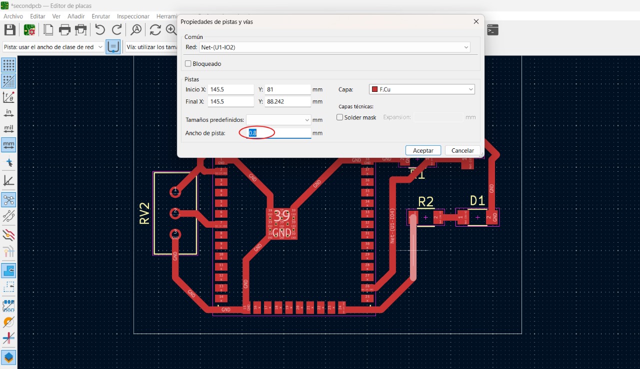
We also need to change the track width. We can do this by "right clicking" and changing the following value
CHECK DESIGN RULES
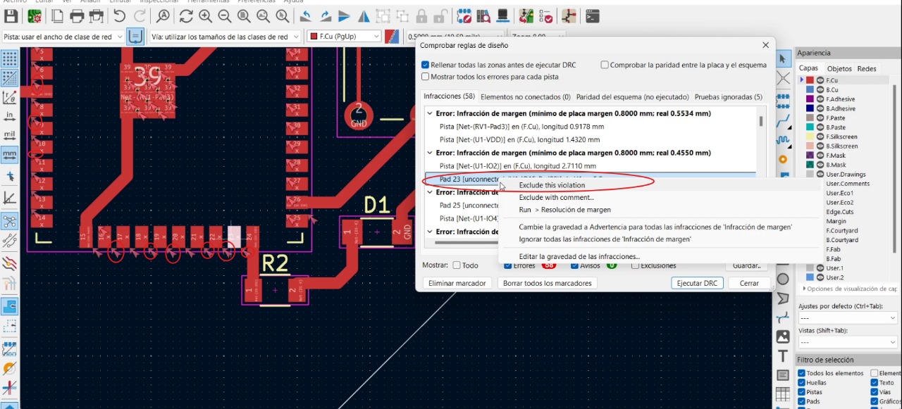
The most common error within the board is that ESP32 pins were not connected. We can exclude them in the following way. The tool is in "Inspect/ Design Rules"
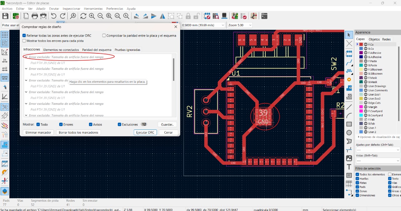
Another error will be the following, we can exclude it as well
ADDING DRAWS
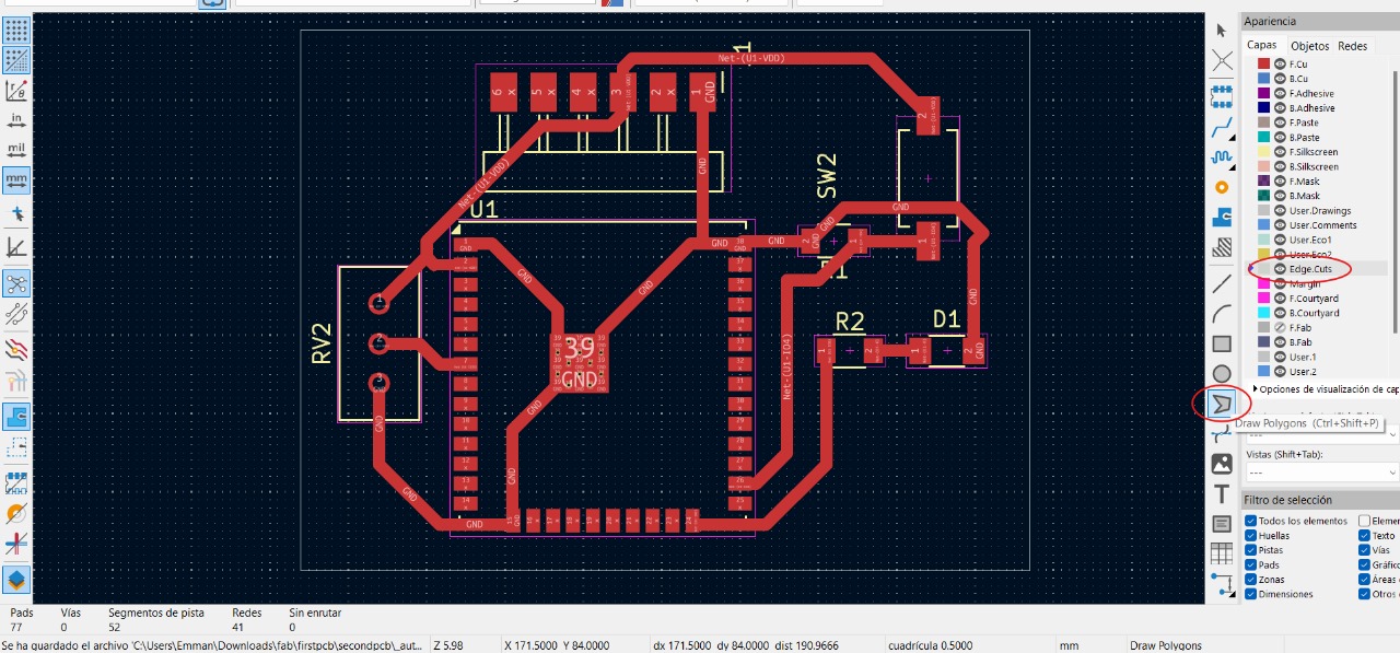
I experimented with different connection configurations. Since it was my first time, I think I understand that it's better to first connect all the components and then create the board design so that it has enough space
- FINAL RESULTS -
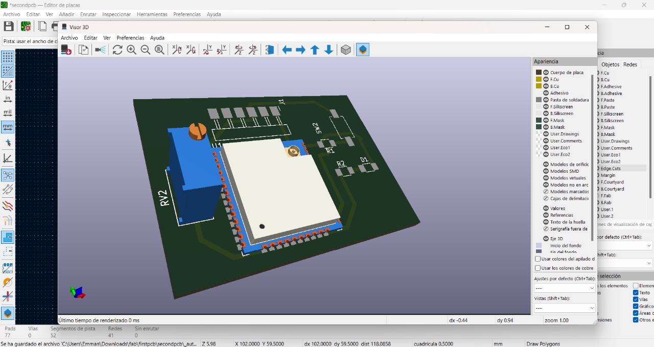
You can see the 3D result of how this would look using the options in the bar: view/ 3D viewer
