8.Electronics Production
This week, I have to create my own PCB.I am excited to see my first physical pcb board.🛸🛸
Group Task:
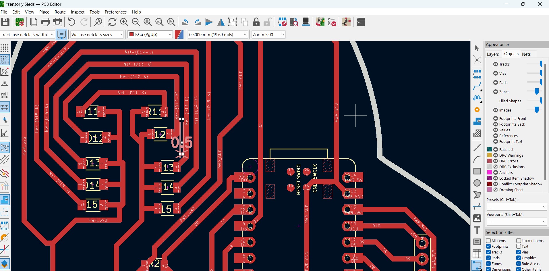
Group task- To start designing my PCB, I check that it meets the following parameters:
- Thick contour lines for cutting. In this case, I set them to 0.8 mm because that is the tool diameter.
- The spacing between traces is greater than 0.4 mm.
- The trace width is greater than 0.4 mm.
- I verify that my components are available.
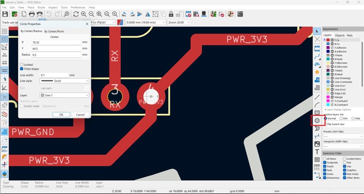
- If I have through-holes, I have to mark them so that the cutting tool recognizes these holes. To do this, I draw a circle on each pin considering its measurement in this case: 0.1mm.
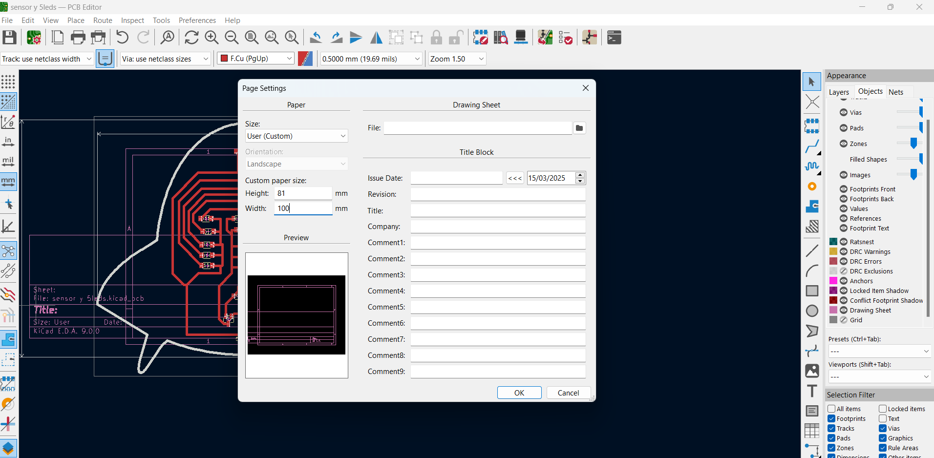
- I Adjusted the PCB area: Modify the area according to the size of my pcb.
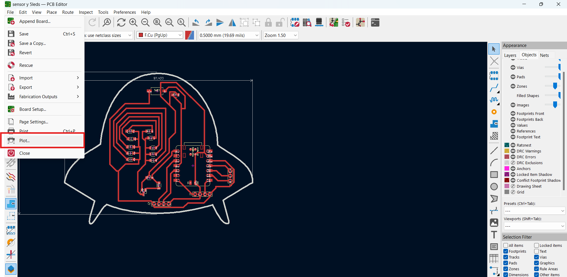
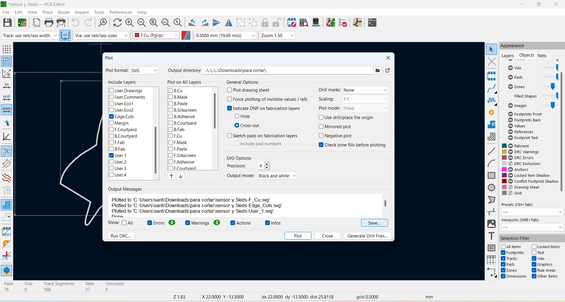
- to export the cuts and the engraving I generated an svg file.To do that, I followed the next steps
- Select the "Plot" option.
- Choose SVG format.
- Select the file.
- Create the plot.
- Save the file.
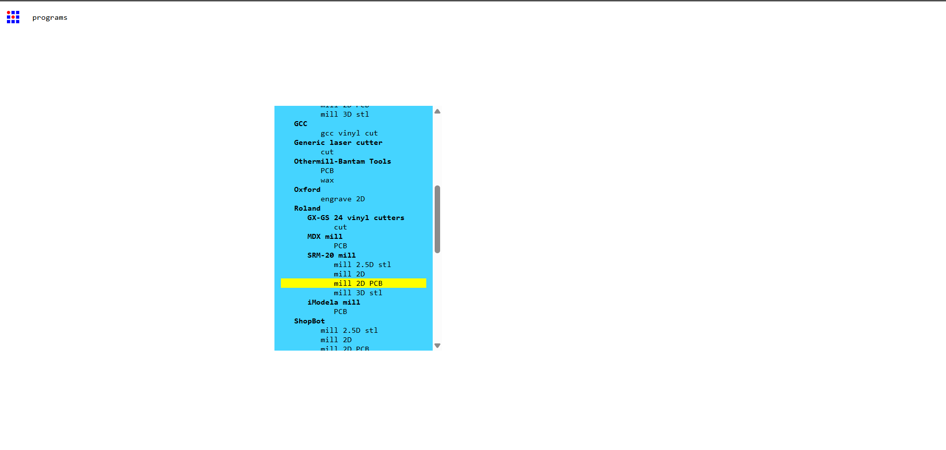
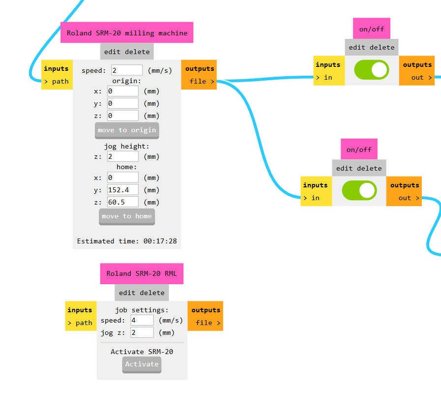
Using mods to create my file .rml
First went to mods, selected the “programs” option and the roland SRM-20 mill PCB.

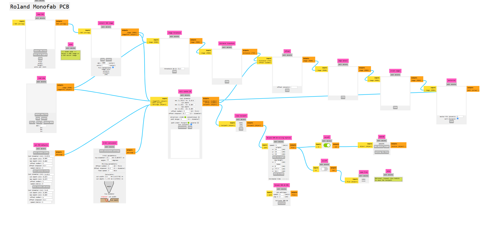
Holes
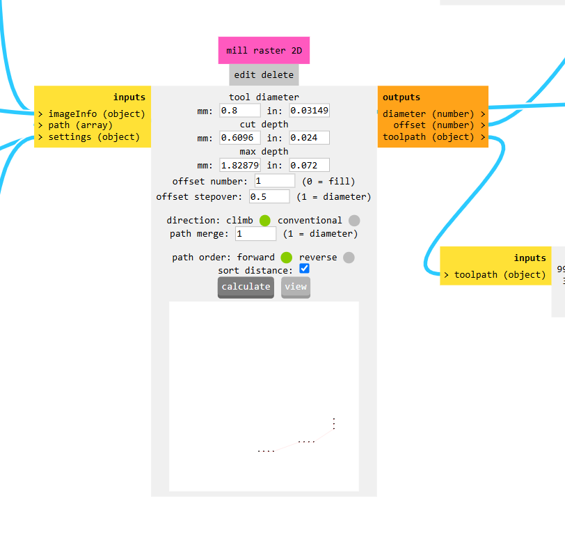
First, I started by making the holes.These are the configurations that I used:
- I added my SVG file.
- I specified the action that I was going to perform. In this case, I wanted to cut the holes, so I used Mill Outline.
- Then, I calculated the parameters, considering that the tool diameter was 0.8 mm.
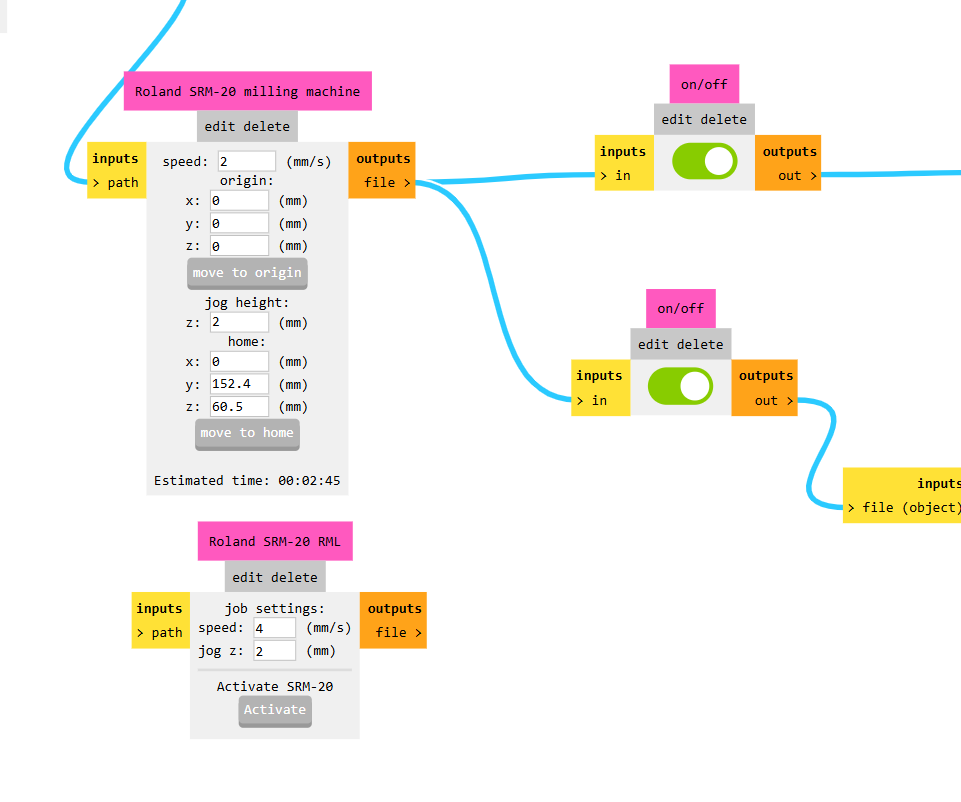
- I set up the speed. I set it to 2 mm because the cut was small, and I considered that the best option was to lower the speed.
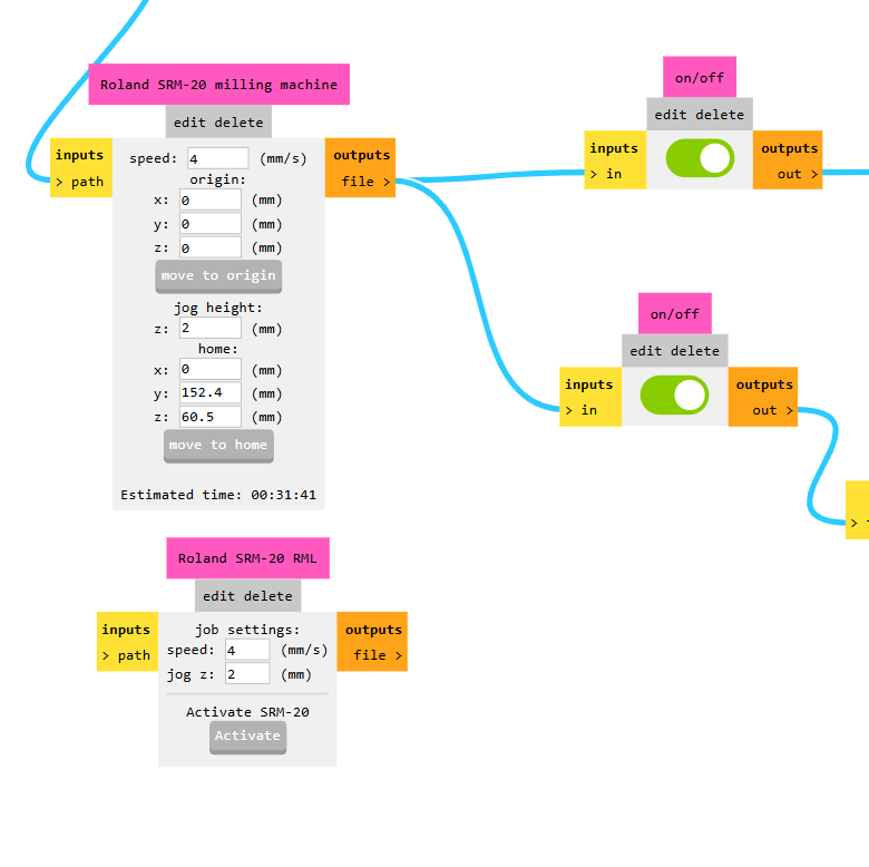
- Finally, I established the X, Y, and Z axes as 0, and I slid the button below so that the program would create an RML file.
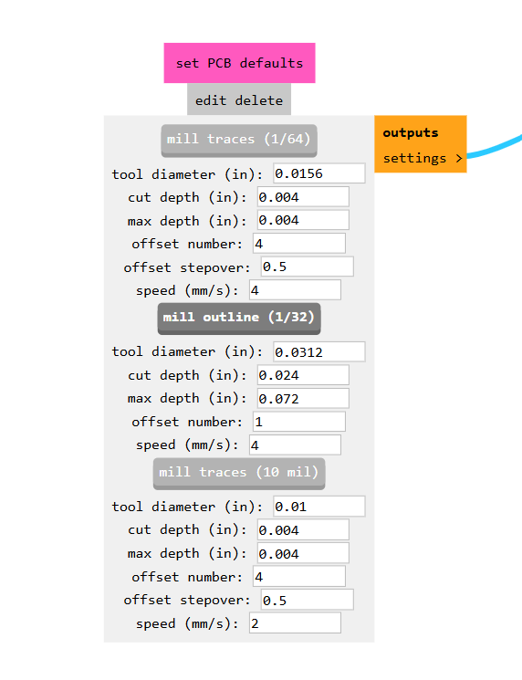
Traces
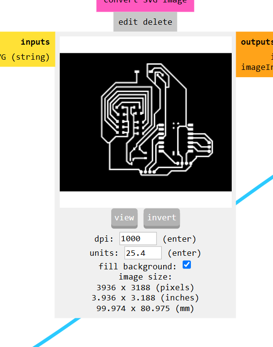
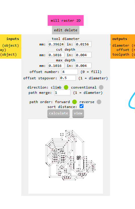
- For the traces, I inverted the image to the machine will engrave the black part and leave the white part high (the tracks)..
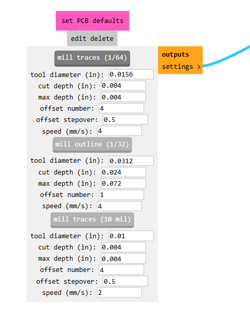
- I set up the action (In this case, it was “mill traces”).
- I calculated the parameters, and I checked that the speed was set to 4 mm/s. I established the axes as 0.
- In this case, the value of 4 indicates that 4 additional paths will be generated, which is useful for cleaning a large area or ensuring that material is removed efficiently.
- Z: 2mm so that when the tool is moved it does not break the material or the tool.
External Cut
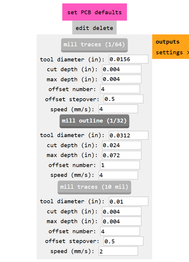
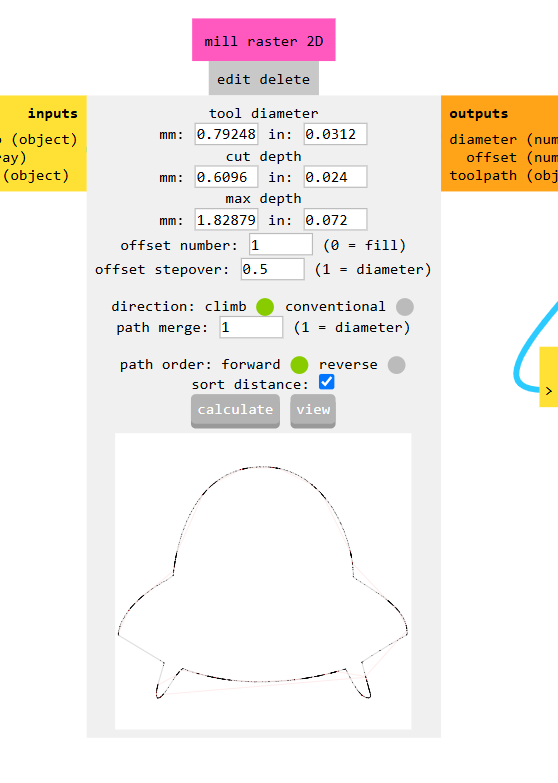
- To do the external cuts, I set up the same as for the holes.
- First, I inverted the cuts, but when I cut my PCB,it did 2 cuts . However, I left a margin, and this didn’t affect my PCB.
These are the correct configurations.
Using the Monofab
I used the Monofab SRM-20
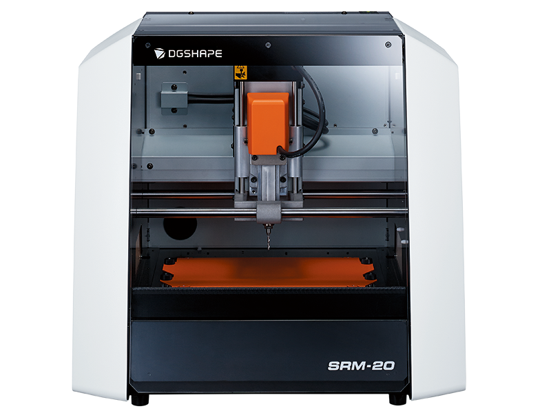
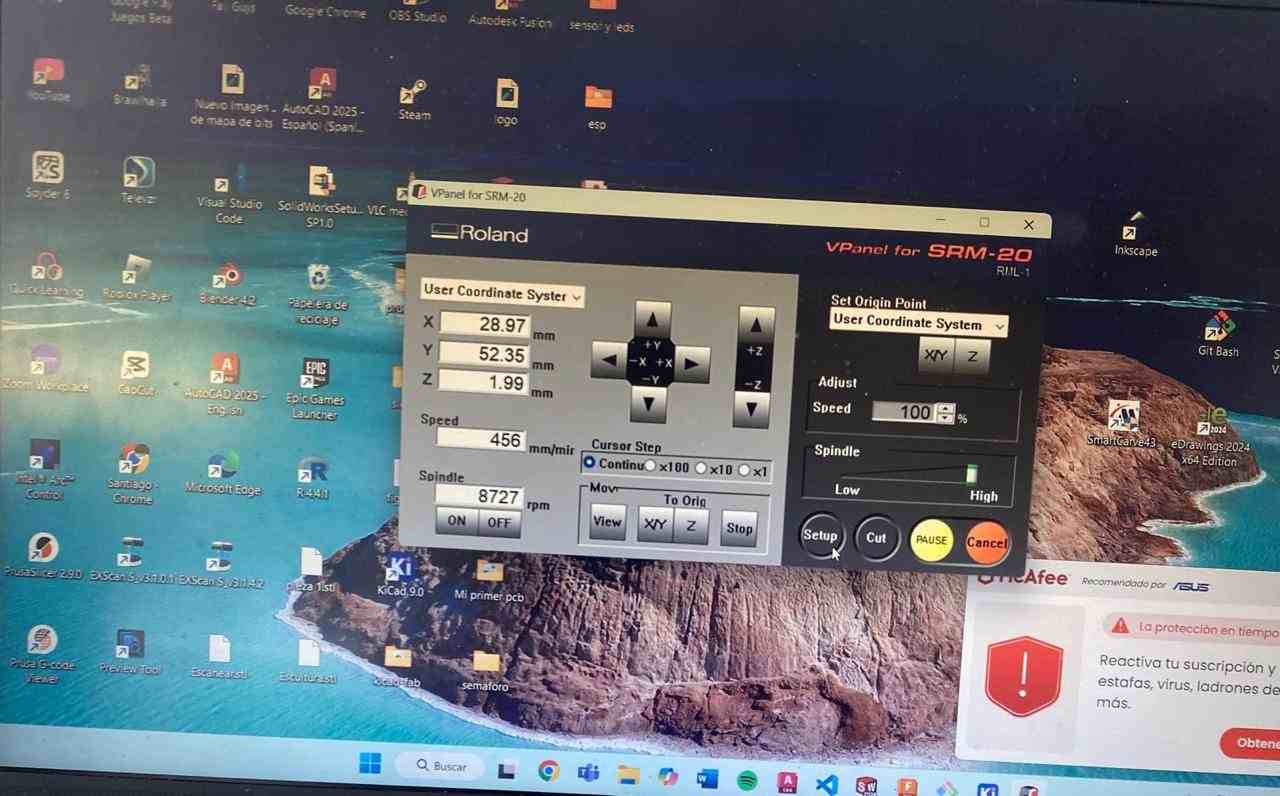
- First, I installed the V panel of the machine ("V panel for SRM-M"), and I connected my computer to the machine.
- Then, I turned on the machine and verified that it was connected.
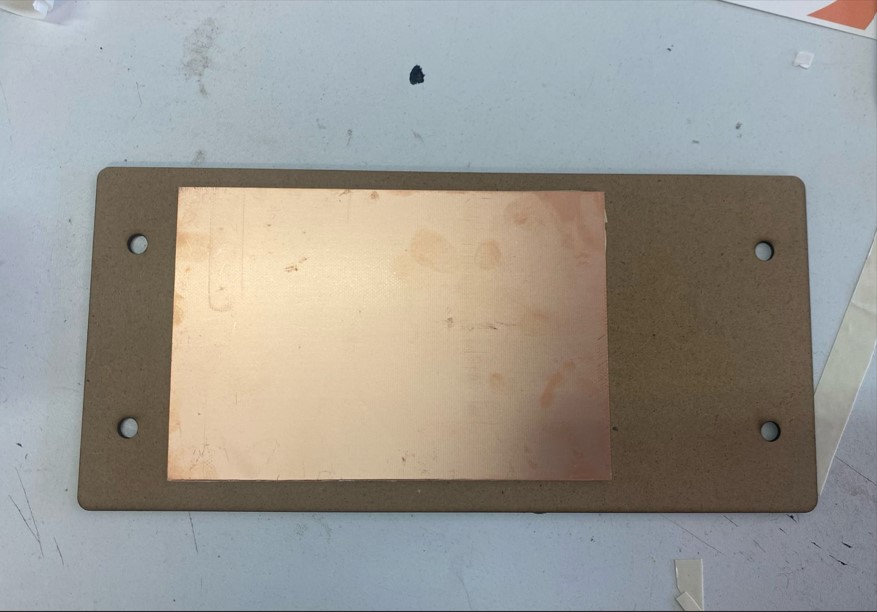
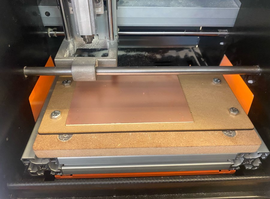
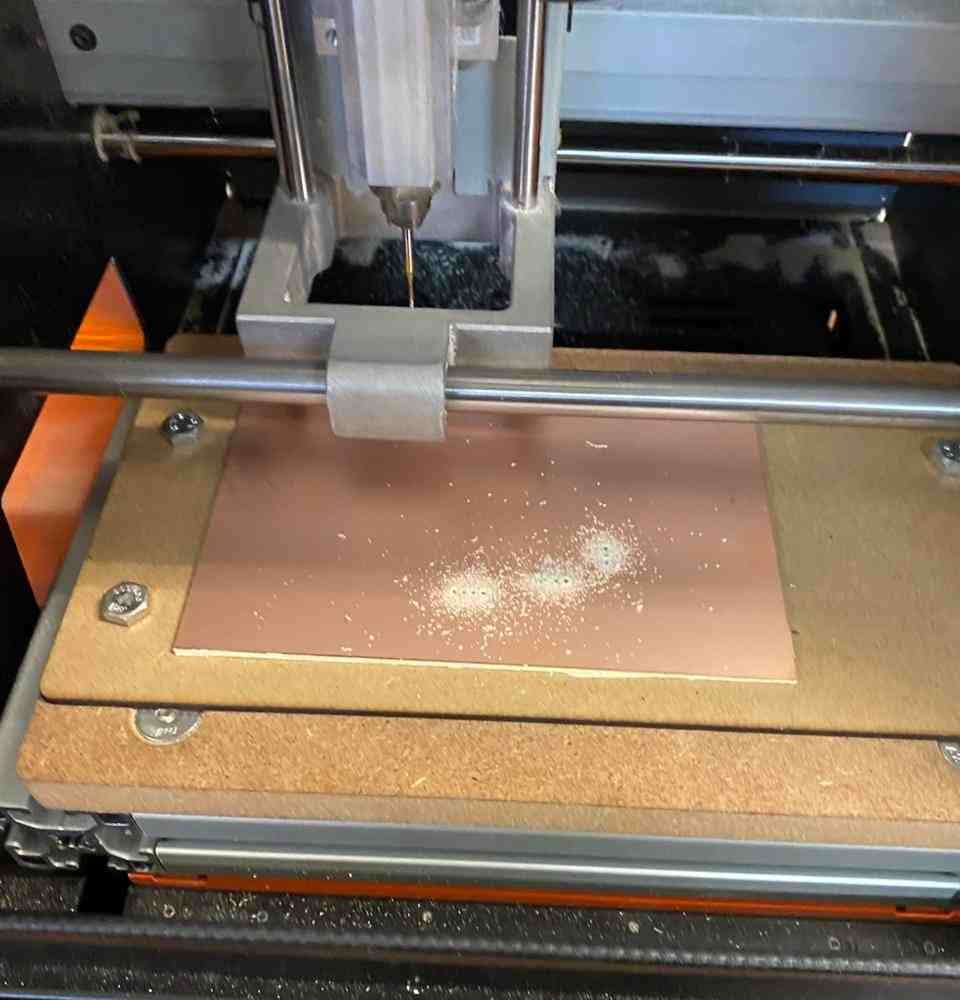
- Next, I used a sacrificial bed of MDF, and I placed my copper PCB in that part.
- After that, I placed the sacrificial bed in the machine and adjusted it with screws.
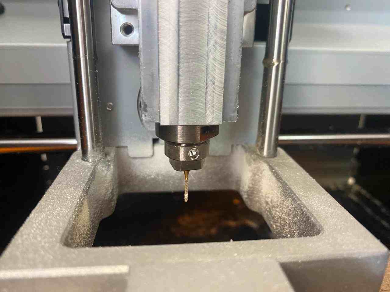
- Then, I checked the tools that I was going to use. The first tool was the cutter, which has a diameter of 0.8 mm.
- The second tool was used to engrave the PCB, and it is in a V shape.
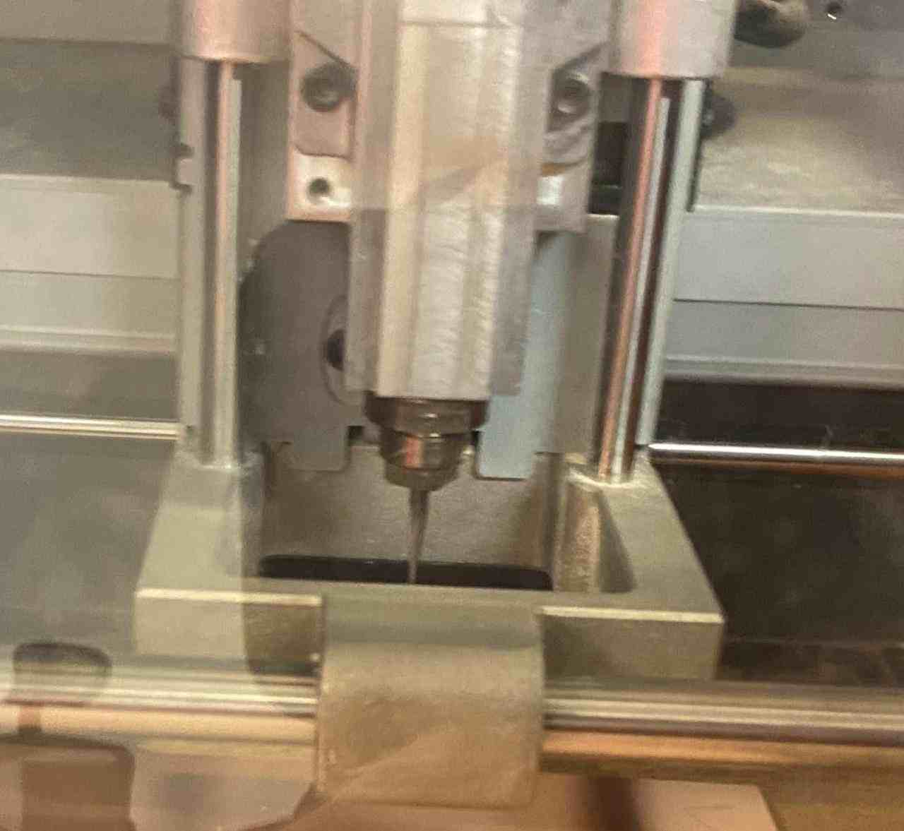
- First, I started by placing the tool.
- To adjust the tool properly, I needed to adjust it well with a star-shaped screwdriver.
- To do these steps, I started by calibrating the axes of the machine. First, I calibrated the Z-axis in the center part to not have problems if the bed is inclined.
- Then, I calibrated the X and Y axes in the lower-left corner.
- To move the tool correctly, there are buttons depending on the distance you want the tool to move. For larger steps, you go to the "continue" option, and for smaller steps, you select the "X1" option.
- To check that the tool is cutting only the required area, placed the tool at the origin and touch the Z and X/Y options to go to the established axes.Then,i moved to the option spindle and turn it on.
- An important thing to remember is that only the tool should touch the plate because you could engrave or cut more than you need.
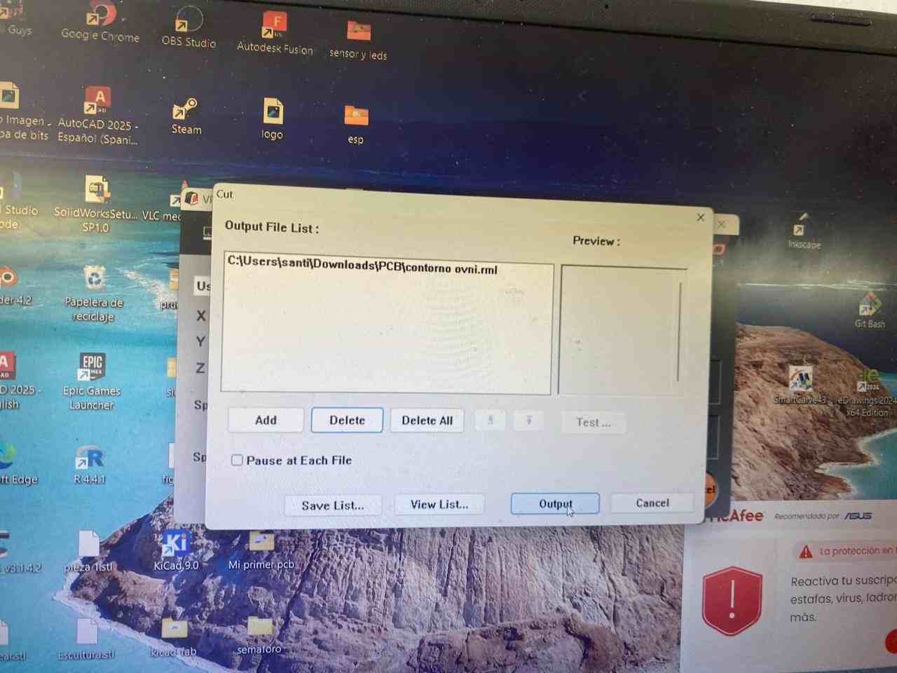
- First, I started with the holes using the cutting tool.I clicked on the “cut” option and selected my file, then I clicked on “setup” and the tool started cutting.
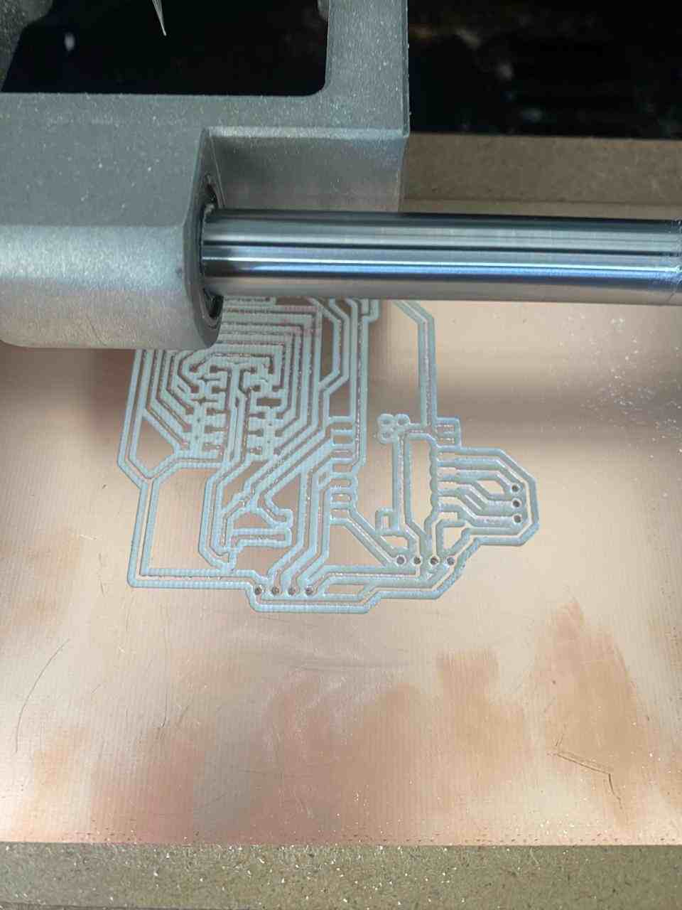
- Then ,I placed the engraving tool and I engraved the traces.
- To do this, I calibrated the Z-axis again because it is a different tool.
- Then, I started to engrave.
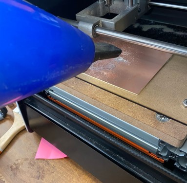
- To remove dust use a vacuum cleaner
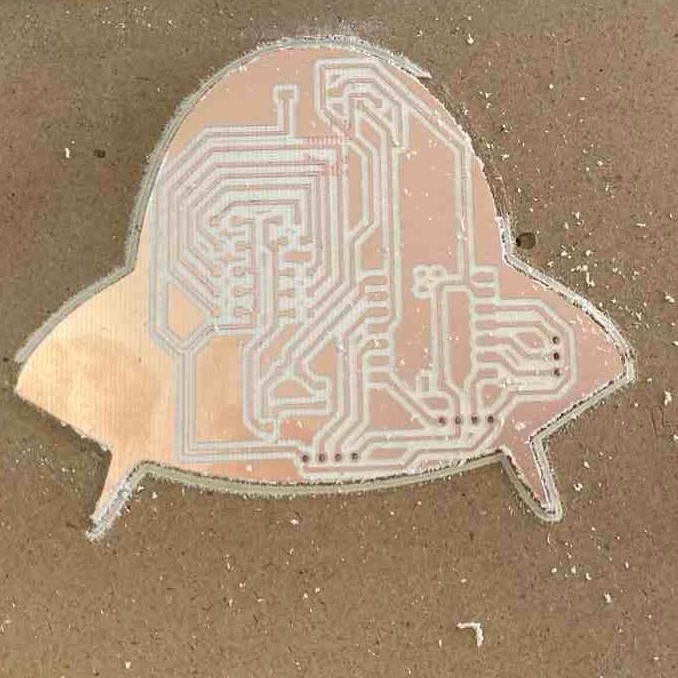
- Afterward, I needed to change back to the cutting tool to do the contour. In this case, it was a cut.
- I calibrated the Z-axis again and started cutting.

My mistakes🛸
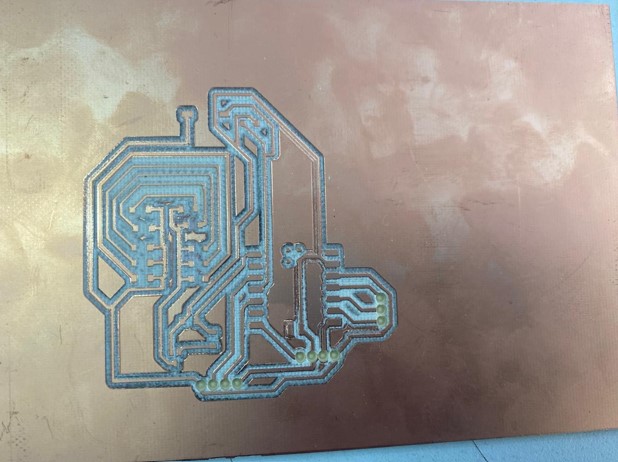
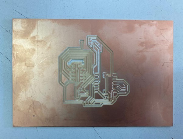
- The first mistake was that I miscalibrated the z-axis and in the engraving, the engraving tool tried to cut and broke the tool.
- In the second problem I did not calibrate the z-axis in the center so the tool did not engrave the strokes very well, so I tried to engrave deeper, but it broke a part of the strokes.
- On the third attempt, I was able to calibrate the tool properly and had no problems.
Soldering
Tools to solder
| Tool | Description |
|---|---|
| Soldering Iron | A tool that heats up to melt solder and join electronic components. |
| Solder Wire | A metal alloy (usually tin-lead or lead-free) that melts to create electrical connections. |
| Flux or Soldering Paste | Helps solder flow smoothly, improves conductivity, and prevents oxidation of components (but a solder wire is like a tube that it has flux in the center). |
| Precision Tweezers | It helps hold small electronic components and wires in place. |
| Desoldering Pump | A tool that suctions molten solder to fix mistakes or remove components. |
| Desoldering Wick (Solder Braid) | It absorbs melted solder, useful for cleaning connections. |
| Multimeter | It measures continuity, voltage, and resistance to check circuit integrity. |
Components to solder
- 1 resistance 330Ω
- 2 resistances 10kΩ
- 5 resistances 270Ω
- 1 Botton
- 5 blue leds
- 1 mosfet N
- 1 Xiao RP2040
- Pins
The calculation of the resistance,I mentioned in Electronic design task
I soldered each component according to my diagram with each tool, and I tested the circuit with a multimeter to verify proper connections before powering the PCB.
- Started with the smallest components first, like the resistors, and finished with the microcontroller and pins.
- Applied a little bit of solder on one pad using the soldering iron, making sure the solder and iron intersected.
- Placed the component with tweezers.
- Fixed the component in place.
- Soldered the other pad.
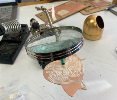
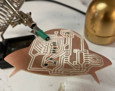
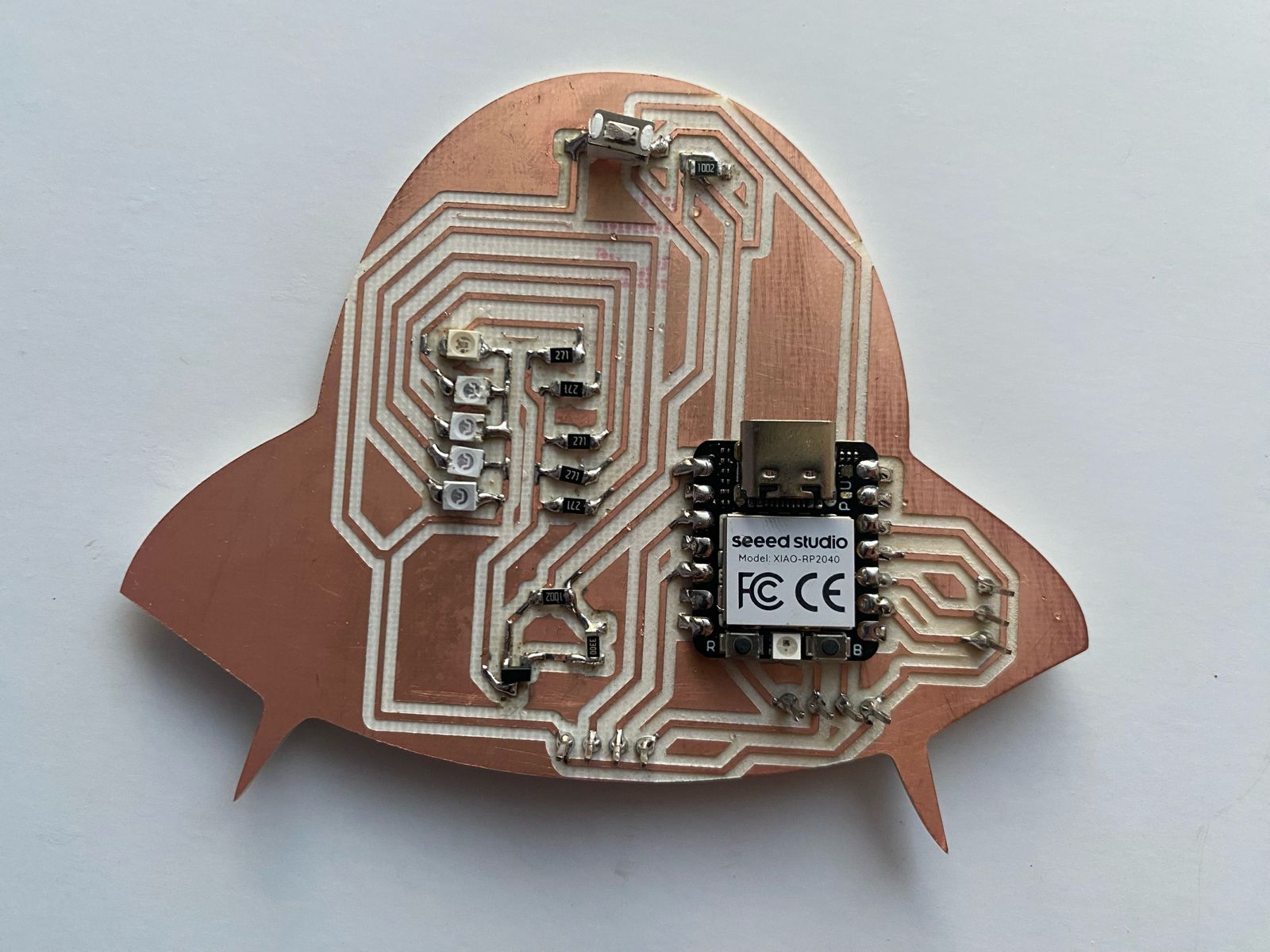
Note: The button is not burned, only a little ink has fallen off.
Programing my PCB
Steps that i followed
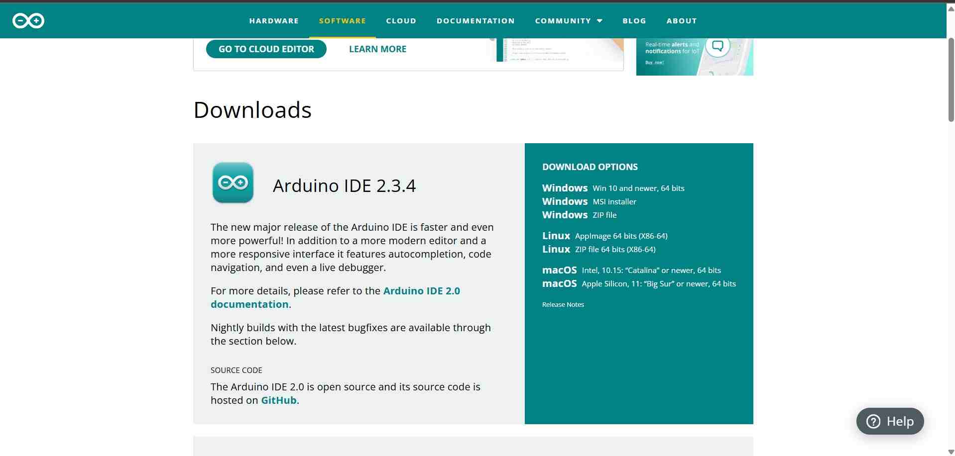
- Install the Arduino IDE
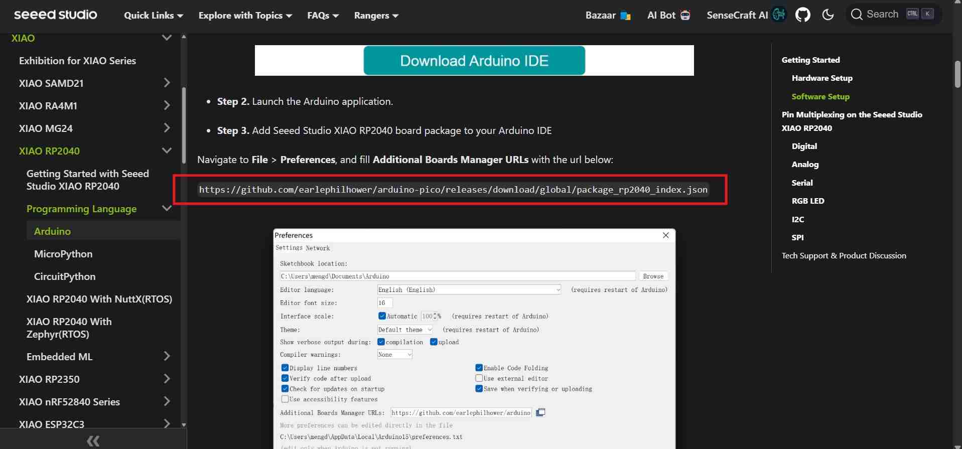
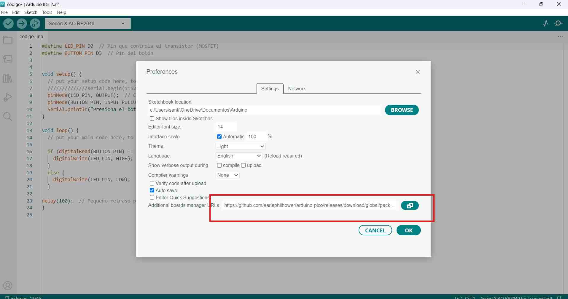
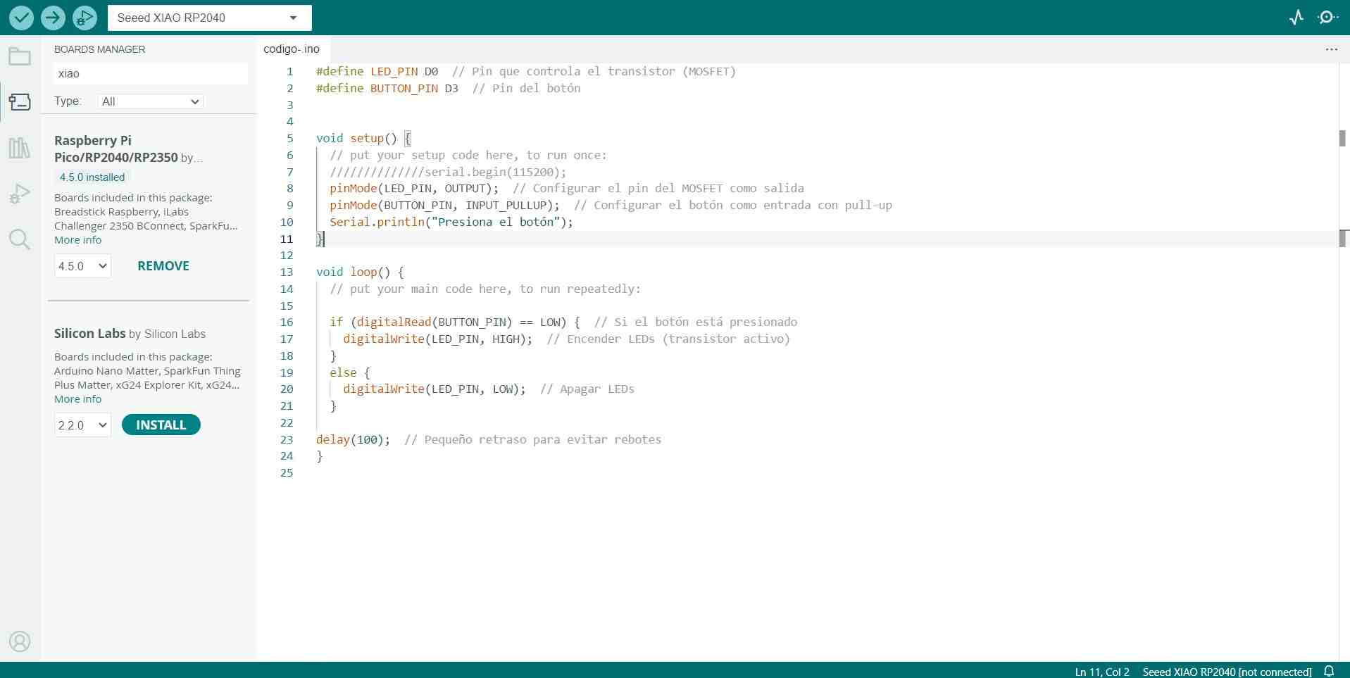
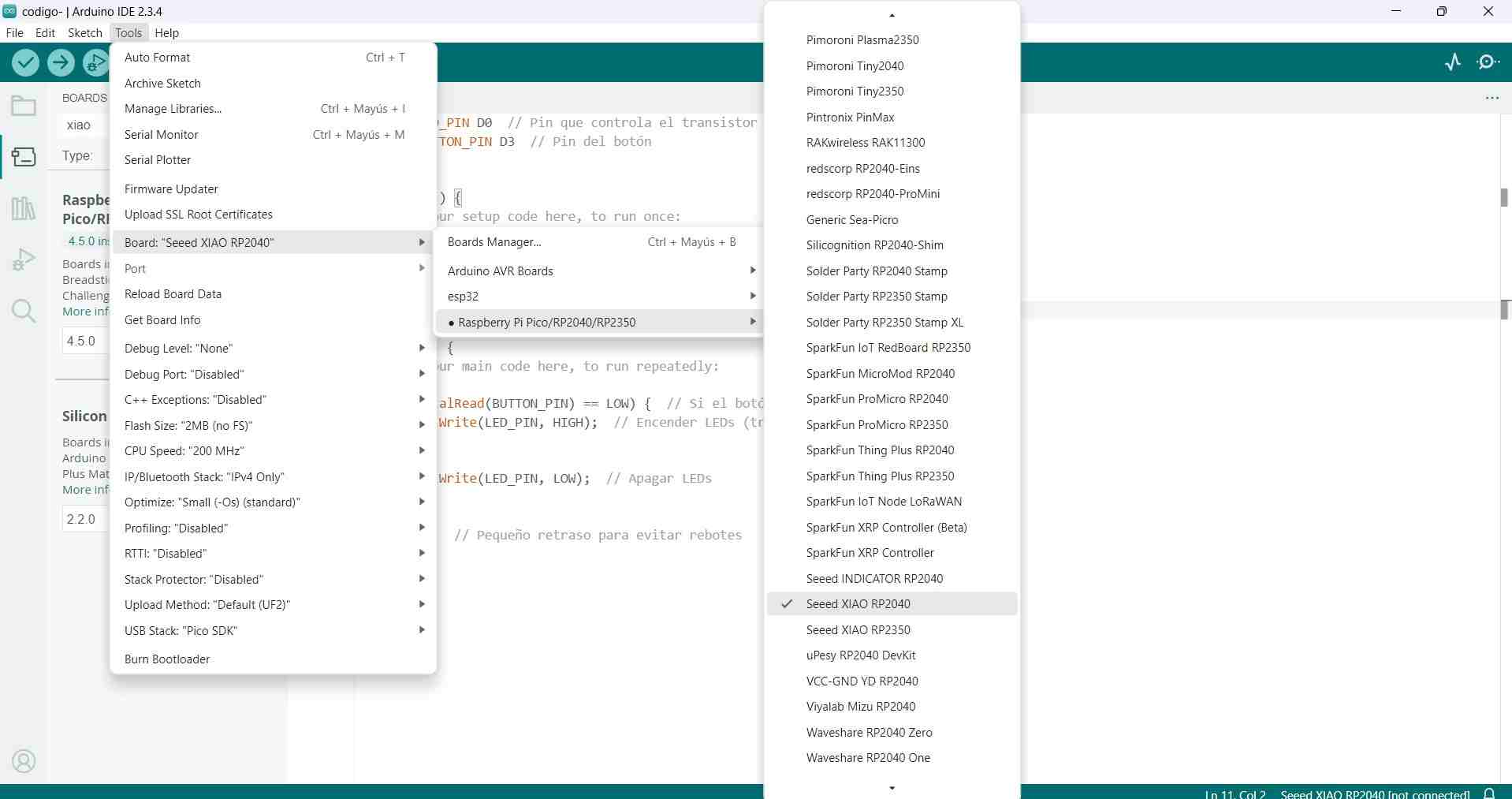
- Add the XIAO RP2040 board by copying and pasting the board manager URL in the Arduino IDE preferences
- Select the XIAO RP2040 board in Tools
- Connect your PCB with the XIAO RP2040 via USB
- Select the correct port in Tools/ Port.
- Start programming and upload your code
Code
#define LED_PIN D0  // Pin that controls the transistor (MOSFET)
#define BUTTON_PIN D3  // Button pin

void setup() {
  Serial.begin(115200);
  pinMode(LED_PIN, OUTPUT);
  pinMode(BUTTON_PIN, INPUT_PULLUP);  // Use internal pull-up resistor
  Serial.println("Press the button");
}

void loop() {
  if (digitalRead(BUTTON_PIN) == LOW) {  // If the button is pressed (LOW)
    digitalWrite(LED_PIN, LOW);  // Turn off LEDs
  } else {
    digitalWrite(LED_PIN, HIGH);   // Turn on LEDs
  }
  delay(100);
}
My PCB working🛸
Files
Conclusion🛸🛸
This was a week with many things to learn in which I had to learn how to calibrate the machine to avoid breaking tools, as well as choosing the right components to avoid damaging my board, soldering small components and programming my pcb. I am happy to see my pcb working.
