6. Electronics Design
This week, I have to design a PCB that uses parts from the inventory to interact.
Group Task:
Group taskcreating my schematic
I use KiCad software.
KiCad is a suite for electronic design automation (EDA).
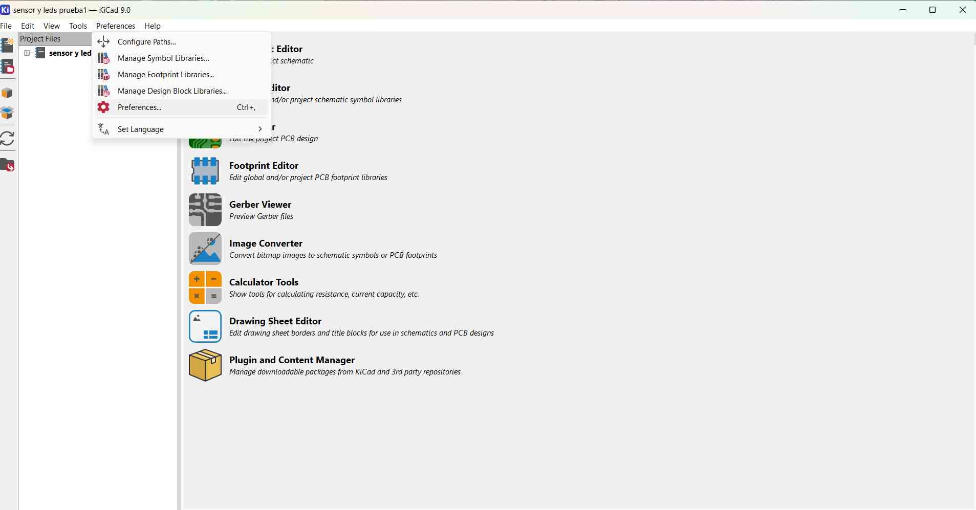
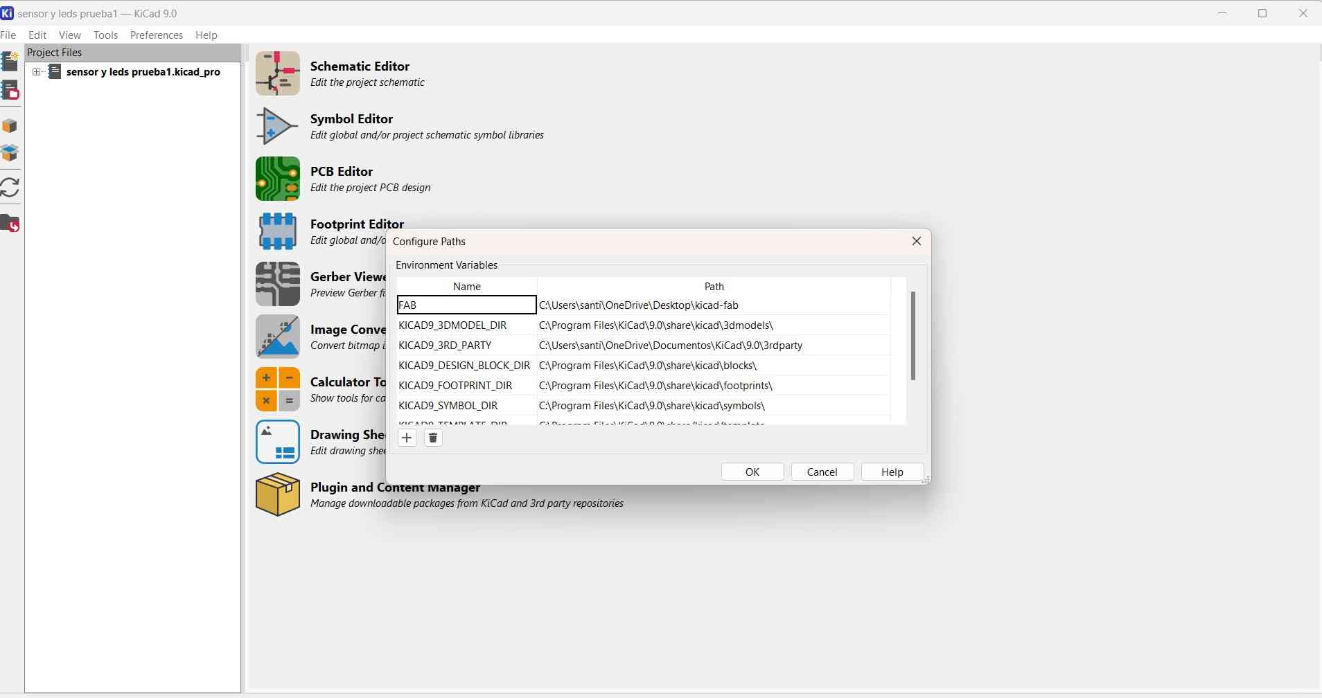
- I imported the library that the instructor gave us.
- I added paths, symbols, and footprints.
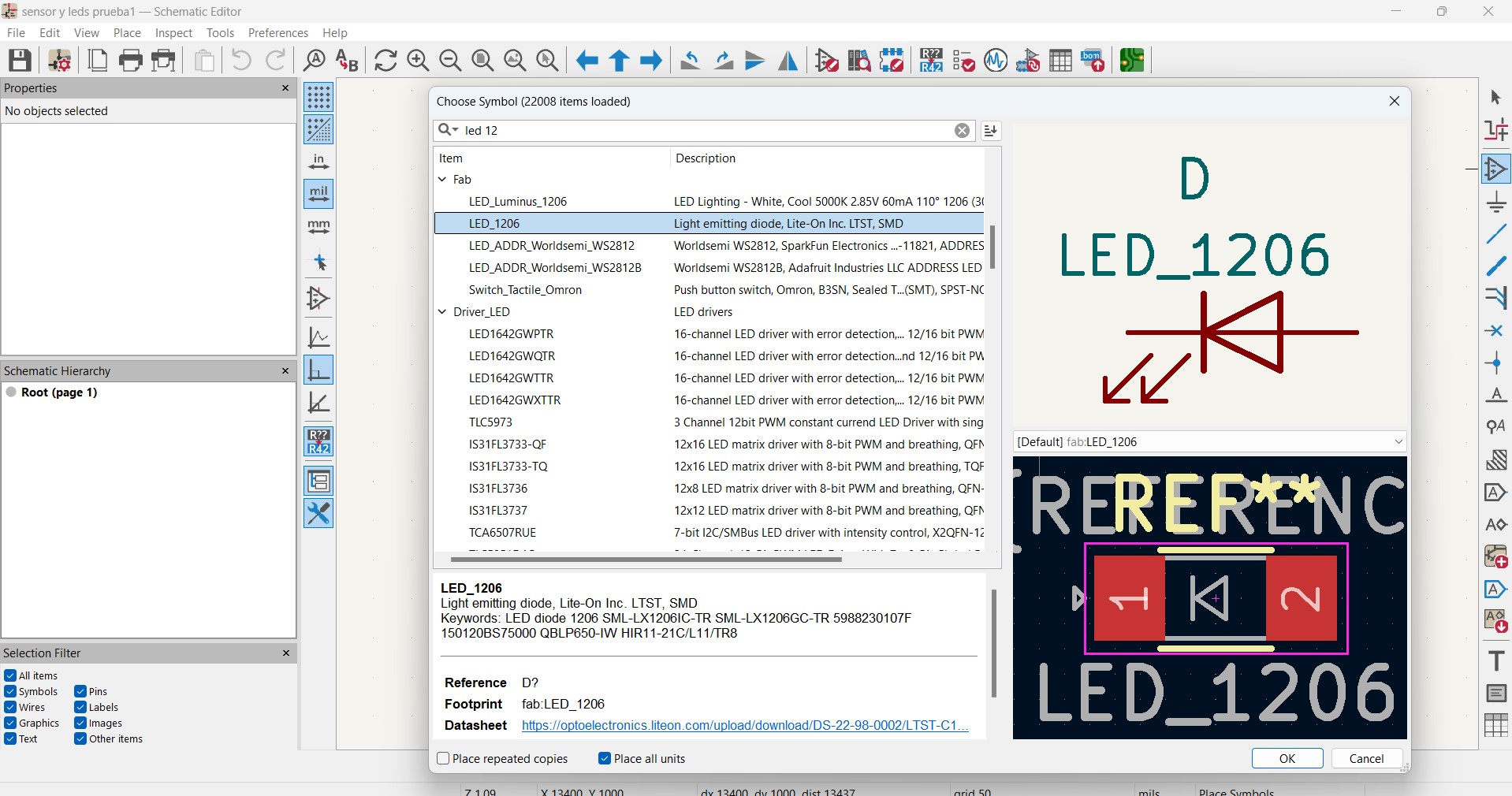
- Inside the schematic, I began by adding components, and for this, I used the "A" key to add a new component.
- In there, you can see the footprint, which is the physical design of a component on the PCB and it is very important to consider the size of your component to be soldered.
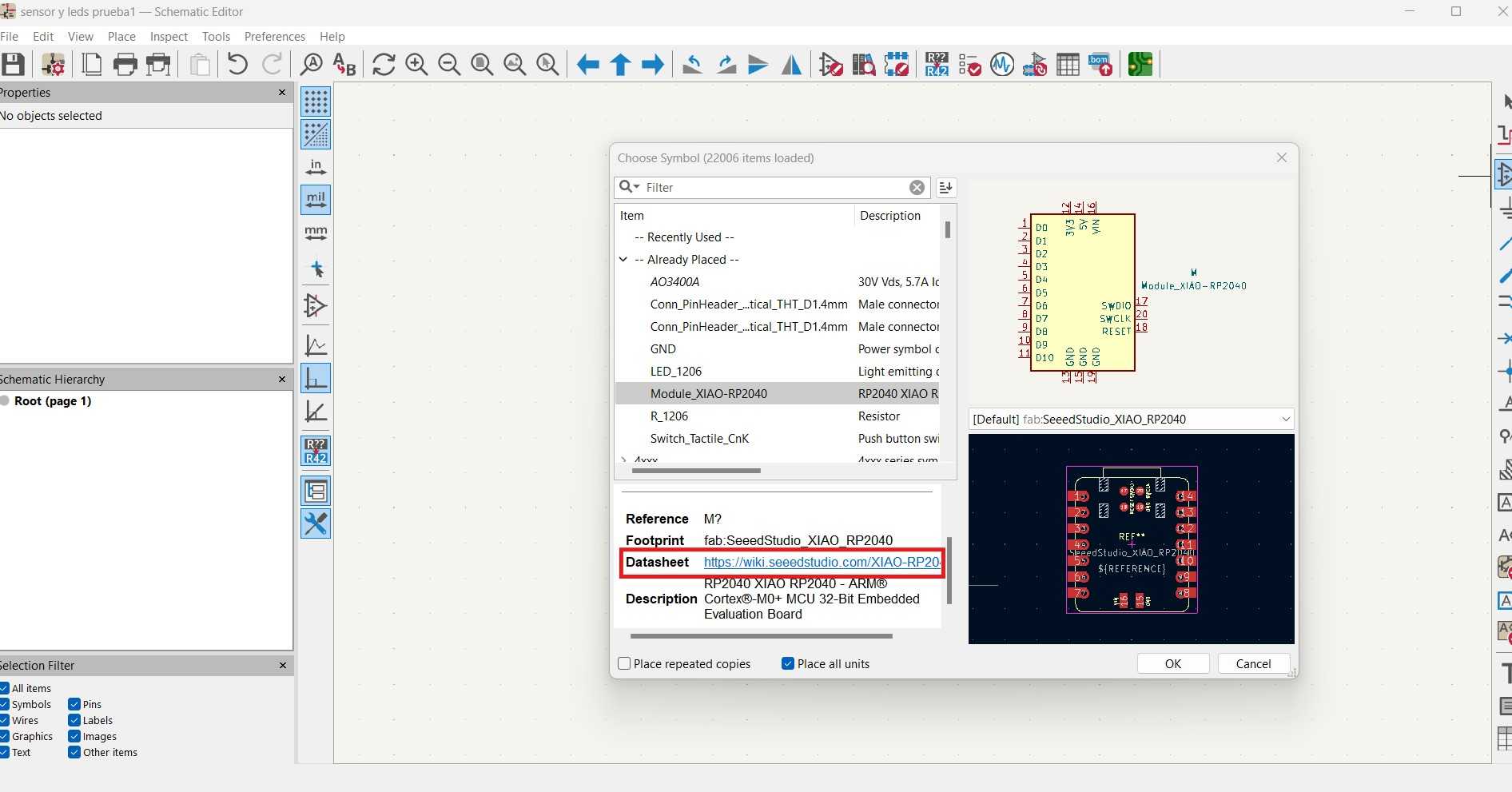
- Other important options include the datasheet, which provides detailed information about an electronic component.
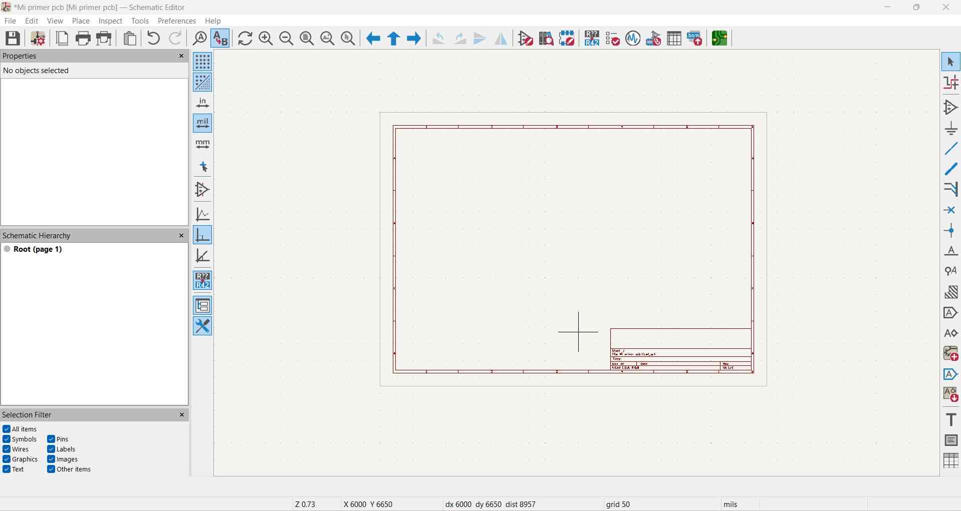
To start creating my schematic, I thought of doing something related to my final project. While I decide, I plan to control 10 LEDs with a button ,add pins for my sensor and Bluetooth communication.
- I started by choosing my microcontroller. I added a Xiao RP2040 microcontroller.
- This microcontroller has the following characteristics:
- Powerful MCU: Dual-core ARM Cortex M0+ processor, flexible clock running up to 133 MHz
- Rich on-chip resources: 264KB of SRAM, and 2MB of on-board Flash memory
- Flexible compatibility: Support Micropython/Arduino/CircuitPython
- Easy project operation: Breadboard-friendly & SMD design, no components on the back
- Small size: As small as a thumb (21x17.8mm) for wearable devices and small projects.
- Multiple interfaces: 11 digital pins, 4 analog pins, 11 PWM Pins, 1 I2C interface, 1 UART interface, 1 SPI interface, 1 SWD Bonding pad interface.
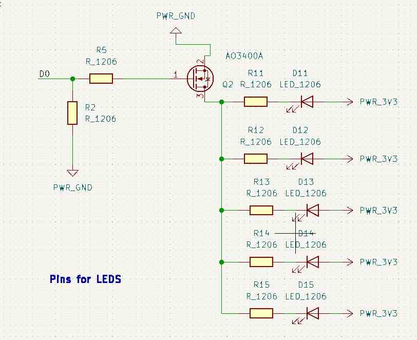
- Then, I decided to add the LEDs. First, I added LEDs with their corresponding resistors to each pin. But this microcontroller doesn’t have enough pins for all the lights that I wanted.
- Next, I searched for how to control the 10 LEDs and found different types of transistors.
- Eventually, I found a MOSFET,This is the AO3400A.
- I considered some values that helped me choose the correct MOSFET:
- The resistance of each LED: 260Ω
- The current for each LED: 10mA
- Voltage: 3.3V
To calculate the resistance,I applied the Ohm's law
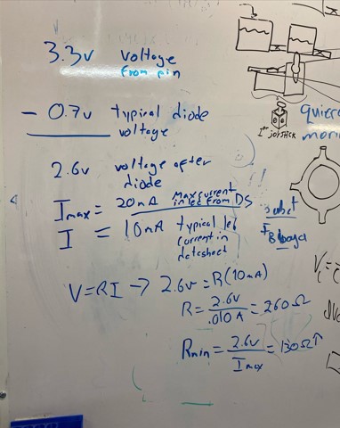
A pin supplies 3.3V, but there is a 0.7V voltage drop across a diode, leaving 2.6V available for the circuit.With this law i can find necessary resistor value to limit the LED current to a safe level.
- For a typical 10mA current, the calculated resistor is 260Ω.
- For the maximum allowed 20mA current, the minimum possible resistor is 130Ω.
I should choose a resistor of at least 130Ω, but a value close to 260Ω is recommended to prevent damage to my LED.
In this case, my LED is blue, with a typical forward voltage between 2.4 and 3 V. For this calculation, I’ll use 2.4 V and a supply voltage of 3.3 V, so the minimum resistor value is 90 Ω for a current of 0.010 A.
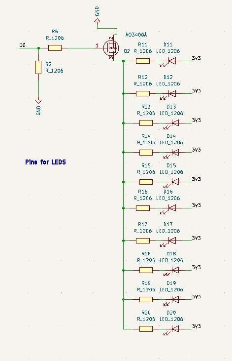
- To control the LEDs, I added a button.
- Resistance (Button - pull-down):10kΩ
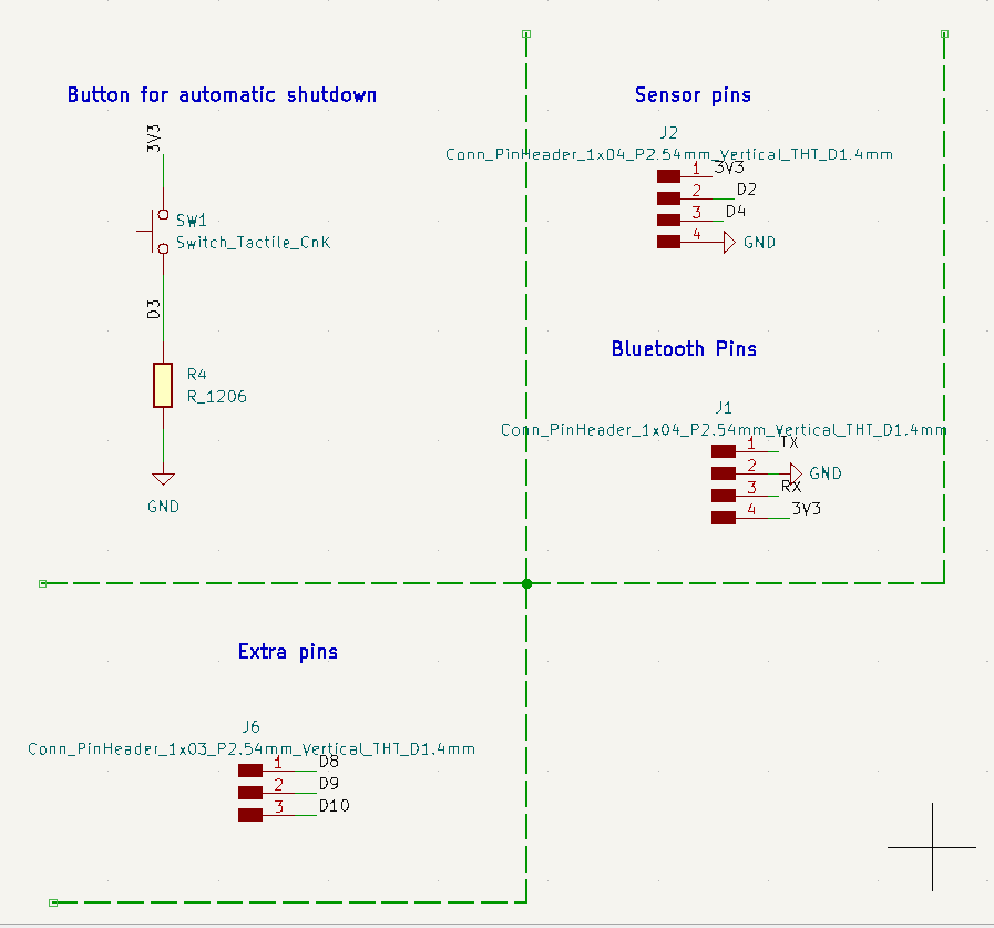
- Now, I added pins for the sensor. I’m going to use an ultrasonic distance sensor.
- I considered 4 pins for the sensor:
- Power source: 3.3V
- Two pins
- GND pin
- Then, I added the Bluetooth pins.
- I considered 4 pins for the Bluetooth:
- TX
- RX
- GND
- 3.3V
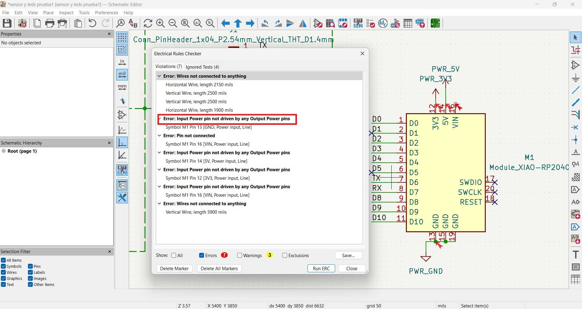
- Finally, to check everything, I used the rule checker.
- The first one is related to the lines (but these lines are only there to organize my schematic, so there’s no problem with that).
- The second one is because it marks the 3.3V and GND pins, expecting a voltage and ground line. However, I’m going to power the circuit with either a USB or a battery later.
I found two repeated errors:
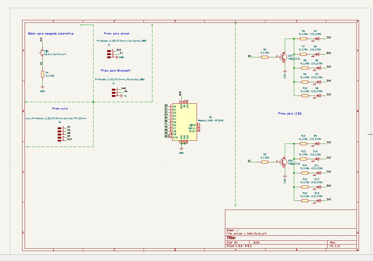
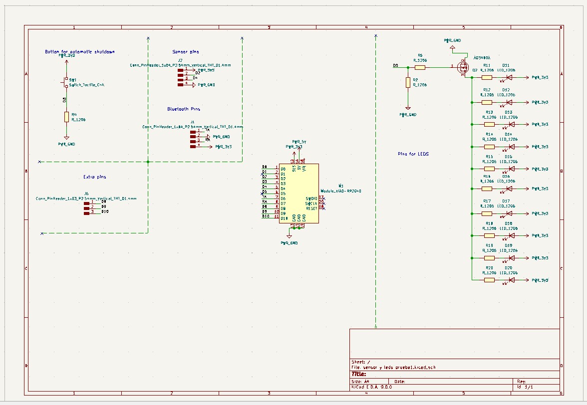
The development of my scheme before and after
Designing my PCB
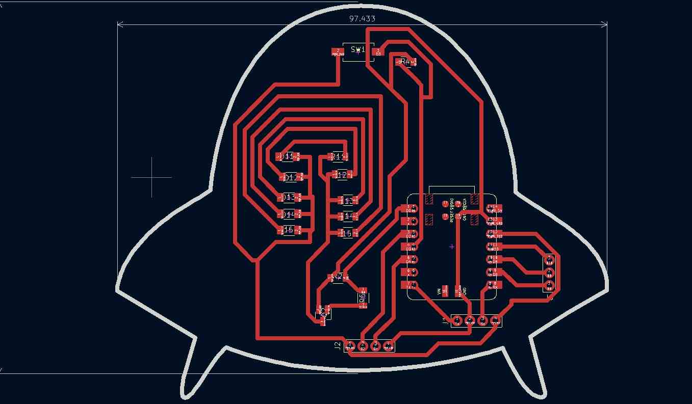
For my design i decided to do a UFO
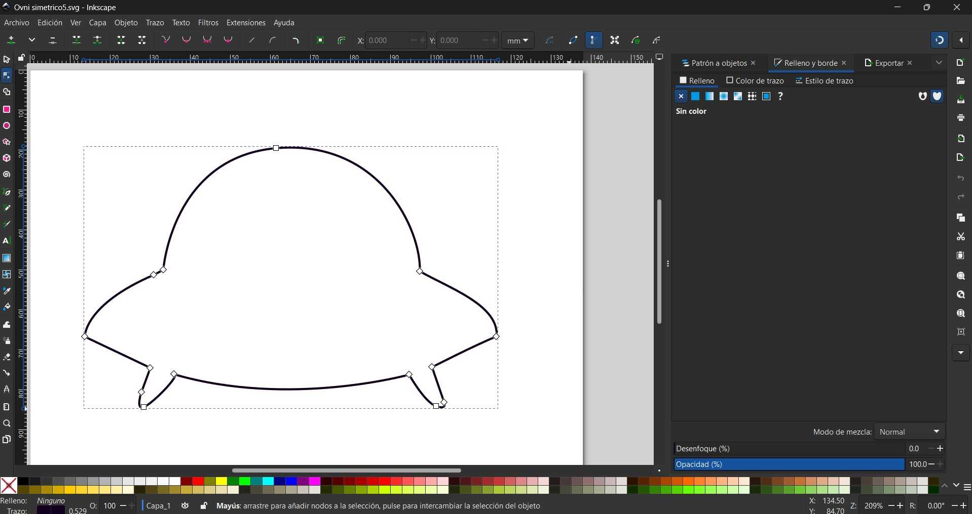
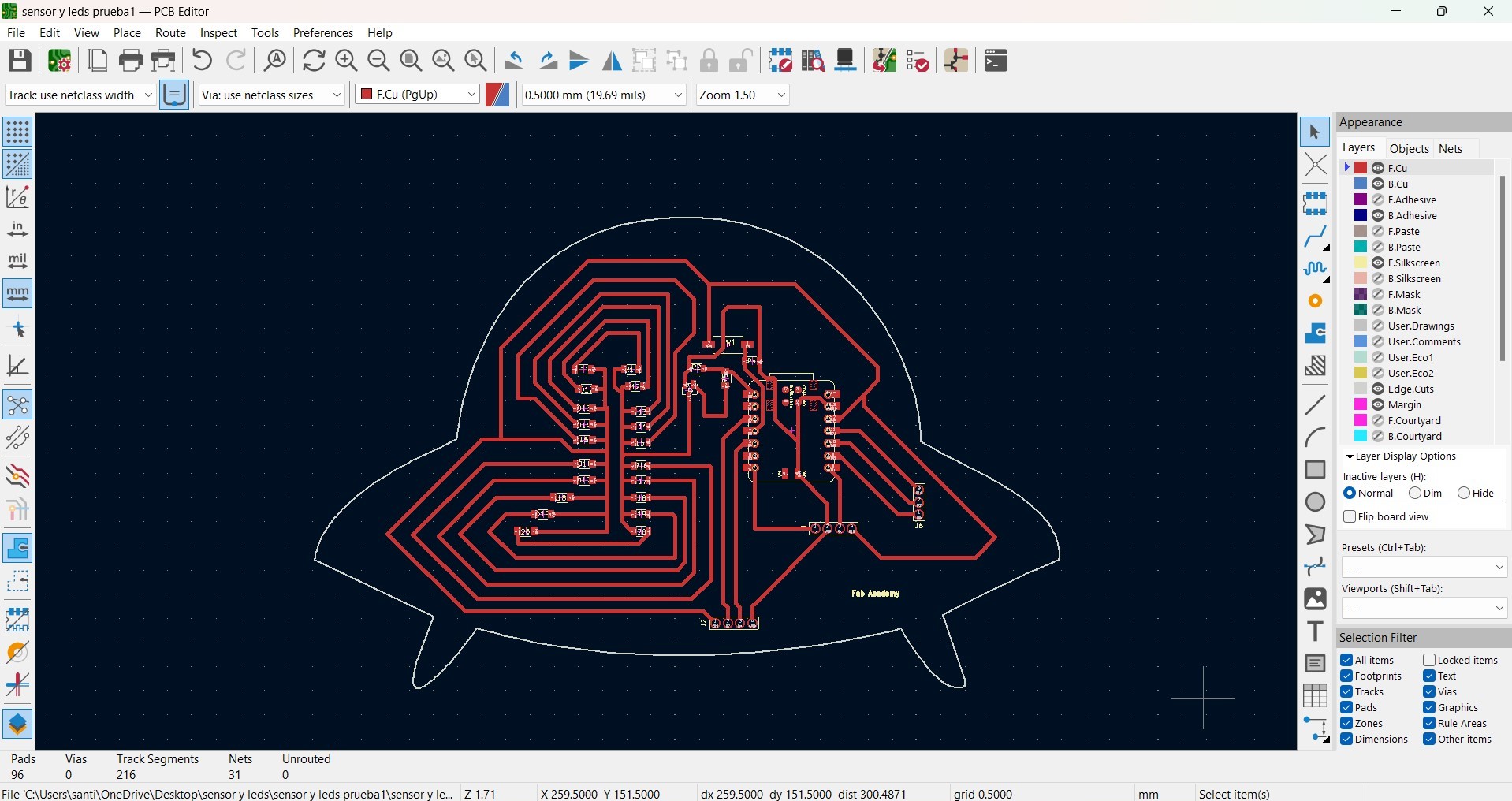
- I created a UFO shape for my circuit(I did the vector in Inkscape.).
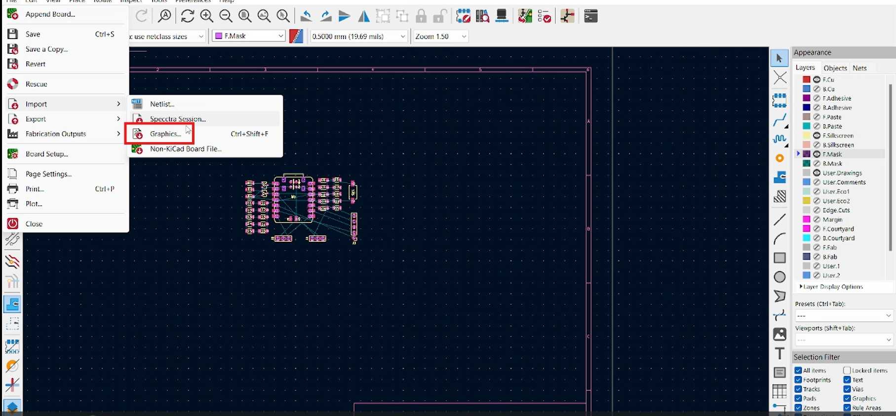
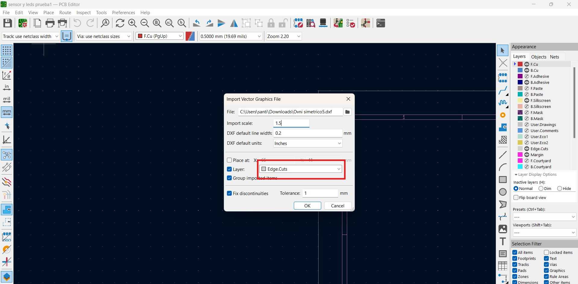
- I passed my schematic and my vector in DXF to my PCB.
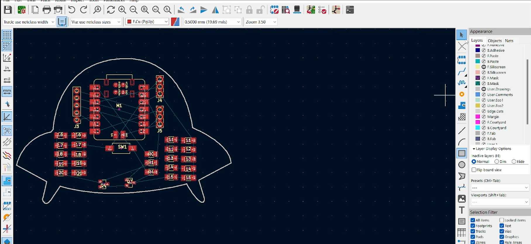
- I started by arranging my components.
- Then, I added the connections and untangled the components.
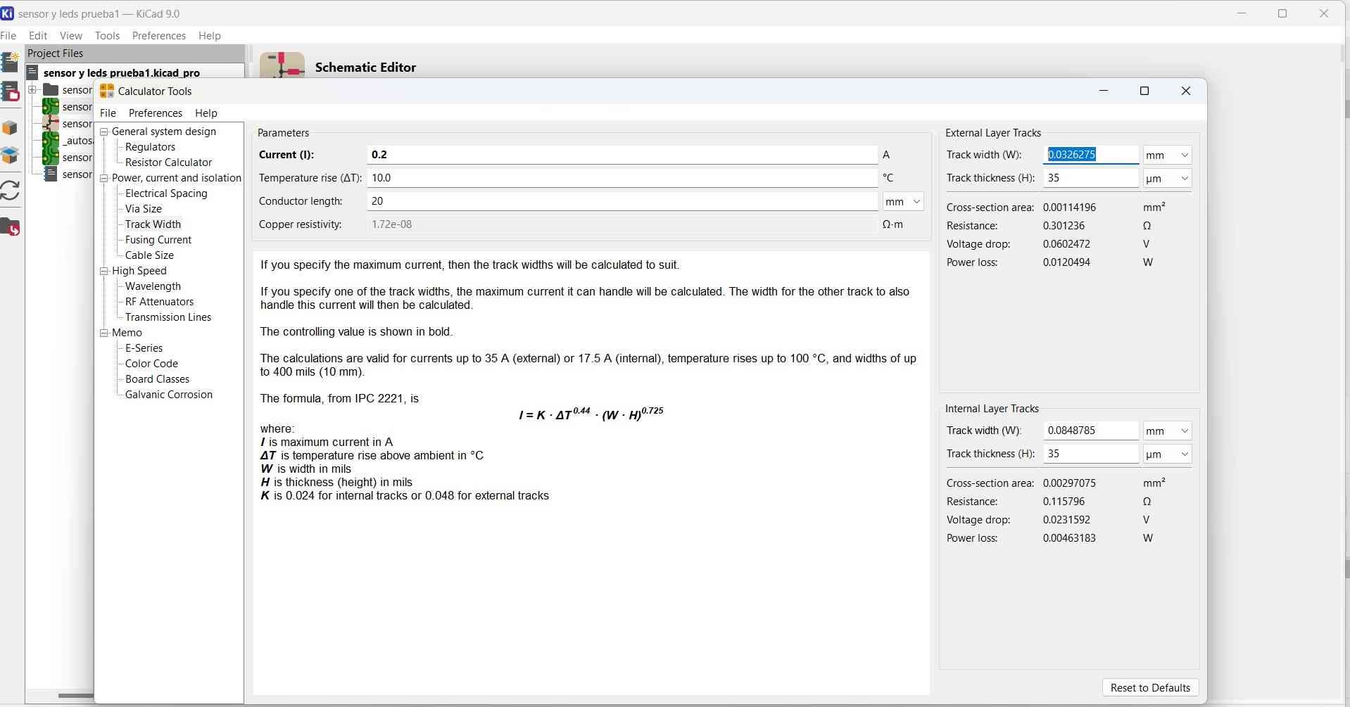
- To calculate the minimum track width, I considered the total current of the LEDs, which is 0.1A. Using this value, I calculated the minimum track width in the KiCad calculator and the established value was in 0.8mm.
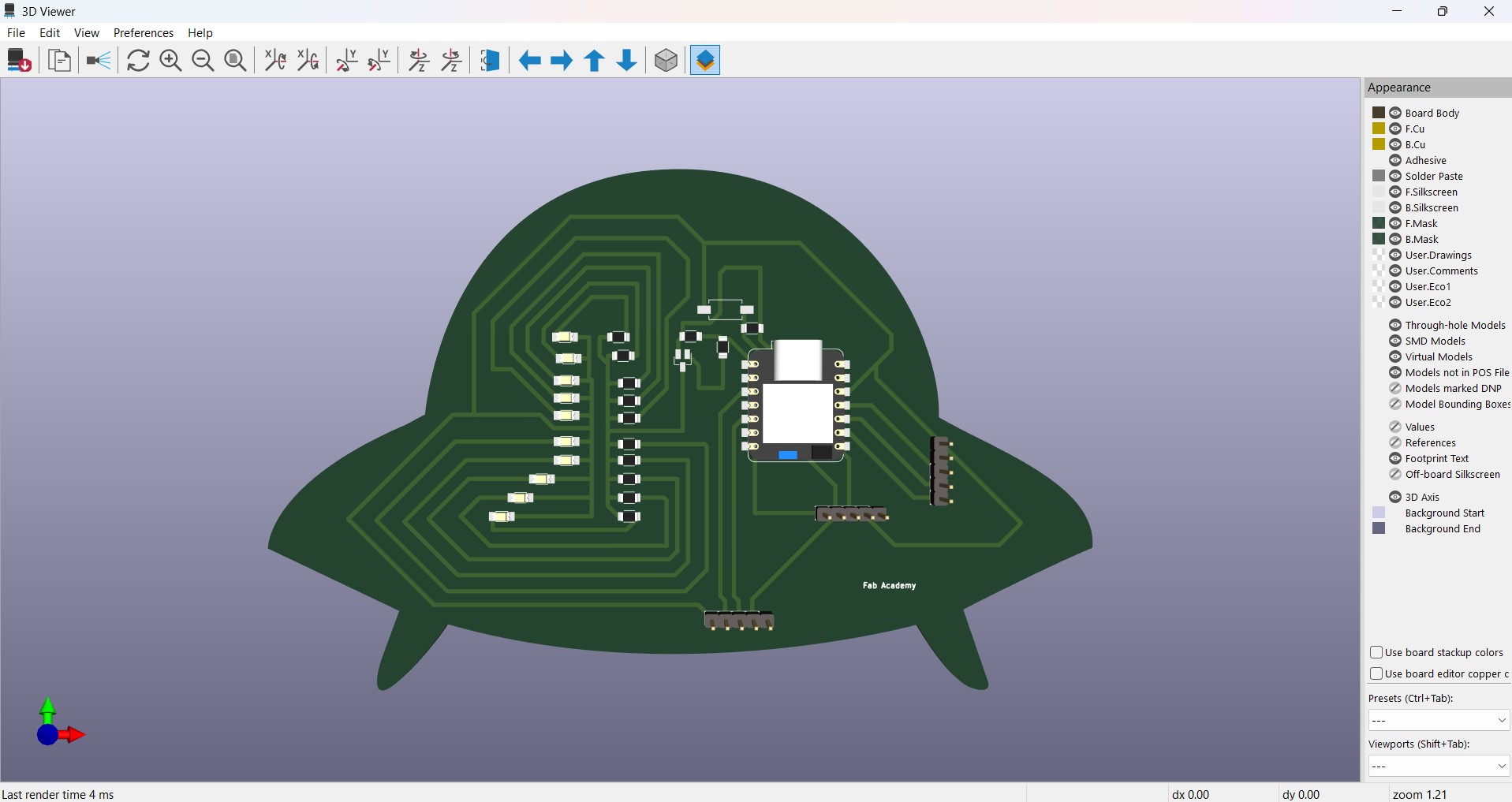
- This is my final PCB.
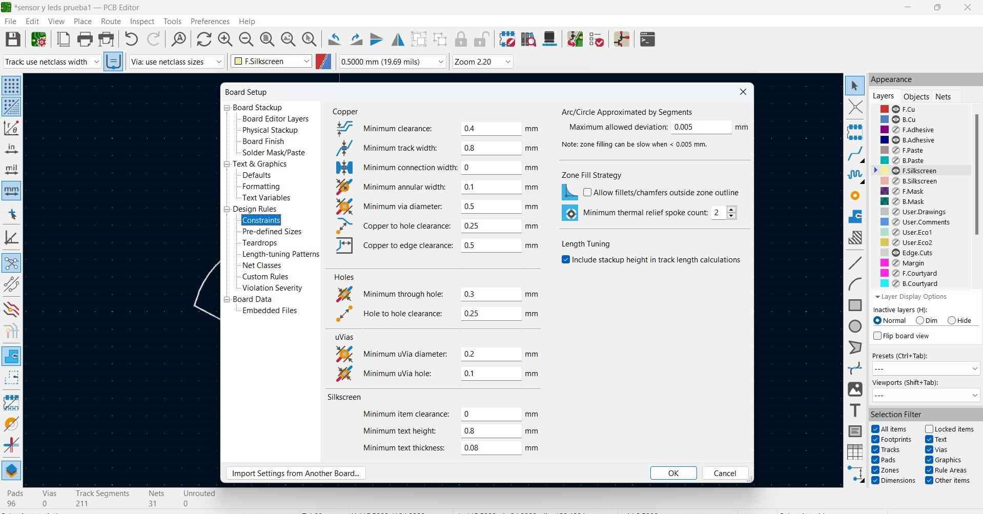
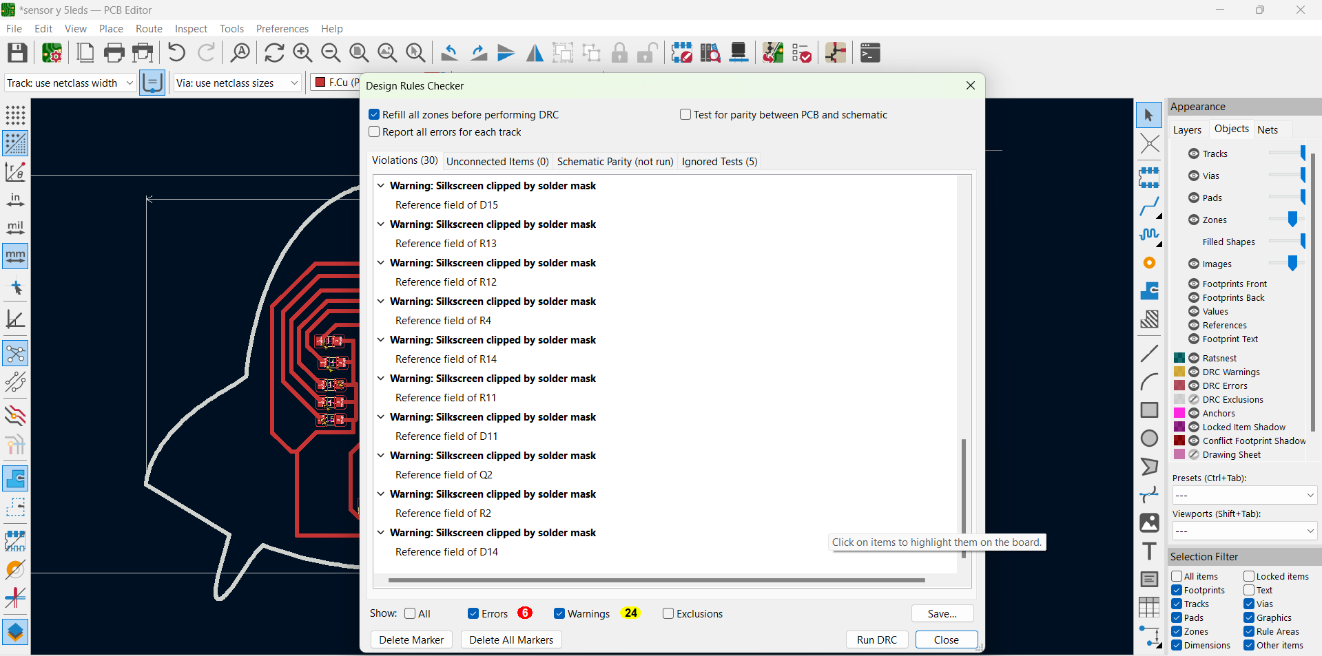
The warnings only affect the silkscreen and text size, which does not influence in the milling and cutting of the routes, vias and edges. Therefore, none of these errors will affect the manufacturing of my PCB, as I will only be performing the milling and cutting process.
Mistakes
- I made mistakes when choosing a transistor for my project because I wasn't understanding the datasheet very well . However, later I was able to understand it and chose the best option.
- Another mistake was that my image wasn’t fully closed, and my vector wasn’t in my PCB layout. Once I closed the lines, everything was solved, and my UFO design was ready. Finally, I can see my shape for cutting.
- I chose an incorrect resistor, but I was able to fix it in time before soldering it onto my PCB.
Changes
- I reduced the LED number to 5 so that my plate was smaller.
Files
Conclusion
This week has been very challenging and enriching for me. Because I had to learn more about the components as well as understand their datasheets better. The hardest part for me was to fit all my components on my board. I will be back in 1 week to see my pcb working.
