Week 9: Input Devices
Objectives
These are the tasks for this week
- Group assignment:
- probe an input device's analog levels and digital signals
- submit a PCB design to a board house
- Individual assignment:
- measure something: add a sensor to a microcontroller board that you have designed and read it
Timeline
Wednesday
- Class by Neil ✔
Thursday
- Class by Saheen ✔
- Designing a PCB for Voice detection (to be continued)
- Documentation (Rough) ✔
Friday
- Designing a PCB for Voice detection (tbc)
- Rough Documentation (Rough) ✔
Monday
- Designing a PCB for Voice detection ✔
- Documentation (Rough) ✔
Tuesday
- Programming (tbc)
- Documentation ✔
- Local Review ✔
Wednesday
Group Assignment
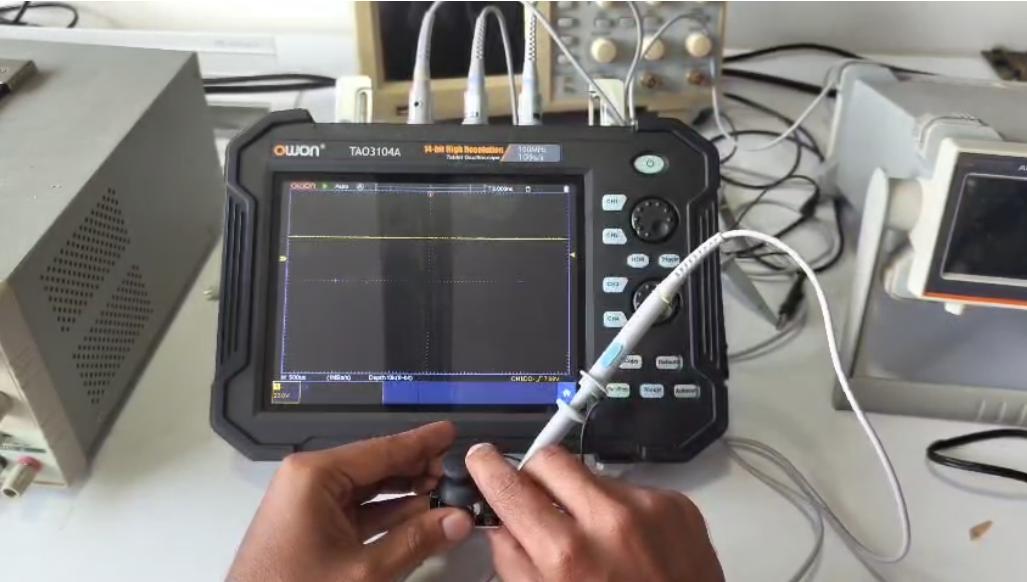
For the group assignment we visualized the signals of INMP441 and P2S Joystick using the oscilloscope. Since we were not able to get clear signals from the INMP441 since it required higher levels of resolution than what we could achieve with our oscilloscope, we used the P2S joystick in which we were able to sucessfully visualise the change in voltage over time.
Here is the link to the group assignment
Individual Assignment
Add a sensor to a microcontroller board that you have designed and read it
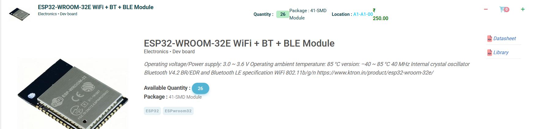
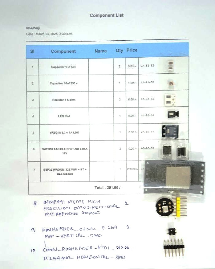
I wanted to make a audio input device that can potentially recognize specific voice commands. For my final project, Lumi should be voice activated. So I wanted to use a MEMS microphone sensor for voice activation. The INMP441 Module is in stock. For control I will be using ESP32-WROOM-32E Module
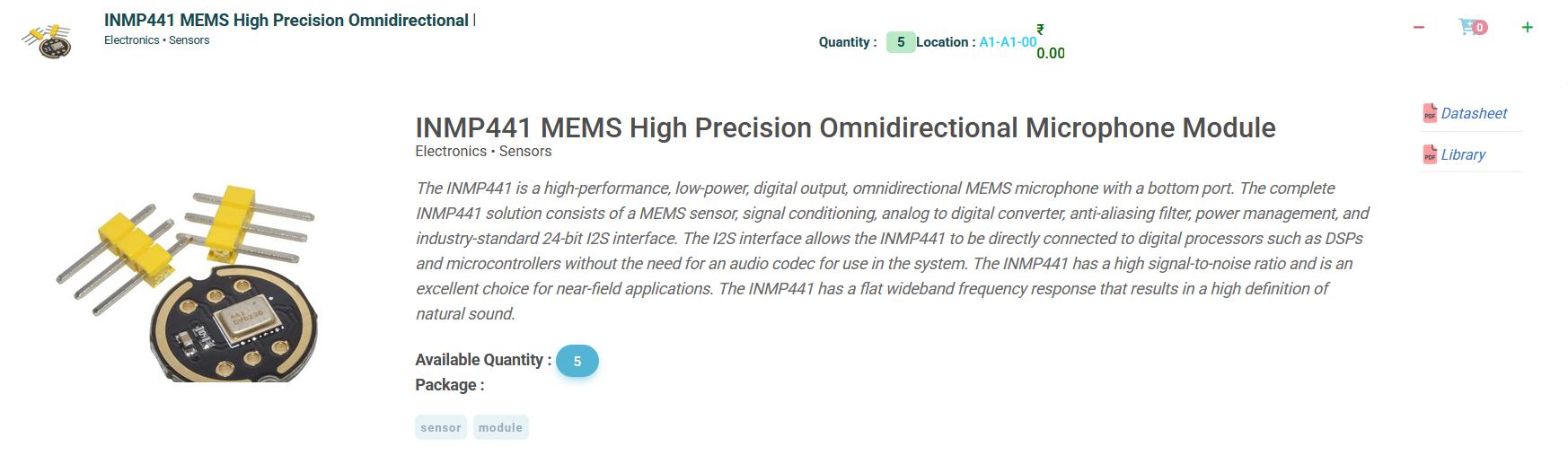
I read through the documentation for INMP441 (without module) and the ESP32-WROOM-32E
The schematic for both components are presented below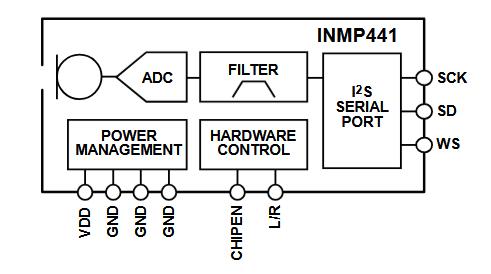
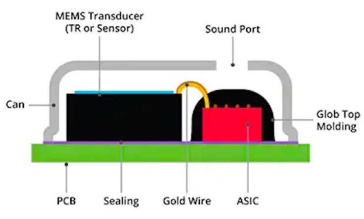
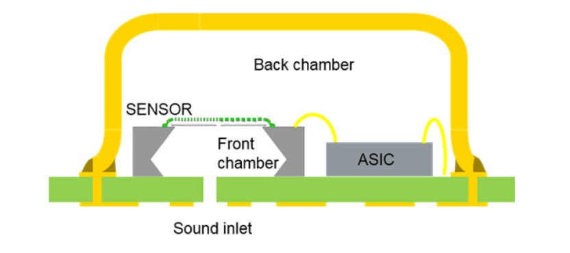
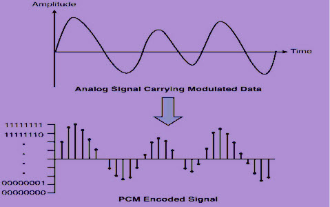
This video by STMicrolectronics provides an overview of how a MEMS (Micro Electro Mechanical Systems) Microphone works. Fist, an anlog audio signal is converted by a preamplifier into a audio signal output. While analog outputs are availabe, one popular option is to perform an analog-to-digital (A/D) conversion to change the amplified analog audio signal to digital signals
In our case, the digital audio is being sent using the inter-IC sound interface (I2S) protocol. I2S is a three wire serial protocol that uses a 'clock' which provides the timing reference to synchronise data transmission, 'data' to send the audio data as pulse-code modulation (PCM) dataand 'word select' line to inidicate which cannel (right or left) is being used for data transmission.
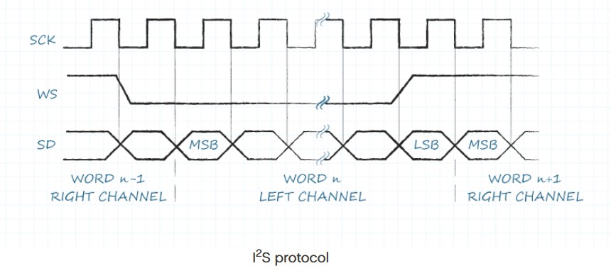
In a PCM data stream, the amplitude of the analog audio signal is sampled at uniform intervals. Each digital step in amplitude is represented by a different set of binary digits, called a pulse code. Each sample is assigned the value of the pulse code that is closest to it in terms of amplitude. So you get a stream consisting of multiple pulse codes that mimic the wave function of the analog audio signal.
I will be using the I2S controller in the ESP32 chip for digital audio using the INMP441
There is two parts to this task
- Make a minimum circuit using the ESP32 chip
- Connect the ESP32 to the INMP441 Module using I2S protocol
Make a minimum circuit using the ESP32 chip
At minimum there shoud be
- pinouts for I2C, UART, and I2S
- connections for Power supply and GND
First add a PWR supply and pinouts for PWR and GND. Since my board requires 3.3V so I need a voltage regulator limited to 3.3V. I look at the documentation and look at Neil's documentation in Week 6 Embedded Programming for reference.
Based on example circuit from AZ1117I-3.3 Linear regulator documentation, I need capacitors of at least 10 and 22 uF in my design. According to the documentation, the ESR (equivalent series resistance, also called internal resistance) of output capacitor should be less than 20 Ω.
Because I did not find any documentation for capacitors, I asked ChatGPT to understand the ESR of the 100 uF capacitor. 100 uF capacitors will have ESR values ranging in milliΩ, so it wont be an issue.
Prompt 1: ESR value of Ceramic Capacitor 100uF 50V..
What is the ESR value of  Ceramic Capacitor 100uF 50V
Electronics • Capacitor

This is 100uF 50V Multi Layered Ceramic Capacitor in SMD 1206 Package. It has X7R as dielectric, which makes up a highly stable capacitor. It has tolerance of 10% only. https://www.ktron.in/product/100uf-50v-multi-layered-ceramic-capacitor/ Multi Layered Ceramic Capacitor Max Voltage: 50V Capacitance: 100uF Tolerance: 10% Dielectric: X7R Manufacturer : Generic
Here’s the response regarding the ESR value of that capacitor:
The equivalent series resistance (ESR) of a 100 µF, 50 V, X7R multilayer ceramic capacitor (MLCC) in a 1206 package is not typically specified by generic manufacturers. However, based on available data and typical characteristics of similar capacitors, the ESR is generally in the range of 10 to 15 milliohms (mΩ). For example, discussions among electronics professionals suggest that a typical 10 µF, 50 V, X7R capacitor in a 1206 package has an ESR around 10 to 15 mΩ. (eevblog.com) Given that ESR tends to decrease with increasing capacitance, it is reasonable to infer that a 100 µF capacitor of the same specifications would have an ESR at or slightly below this range.
For precise ESR values, it is advisable to consult the datasheets of capacitors from reputable manufacturers, as ESR can vary based on specific design and manufacturing processes. Manufacturers like Murata provide tools such as "SimSurfing" that allow users to explore detailed characteristics, including ESR, of their capacitors. (murata.com) Additionally, KEMET's X7R dielectric capacitors offer detailed specifications in their datasheets, which can be referenced for more accurate information. (content.kemet.com)
Given the lack of specific ESR data for the generic capacitor in question, measuring the ESR using appropriate equipment is recommended for applications where this parameter is critical.
For information on other peripherals, I also used this link provided by Namita (FA'25).
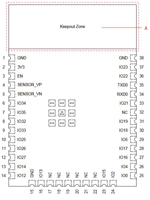
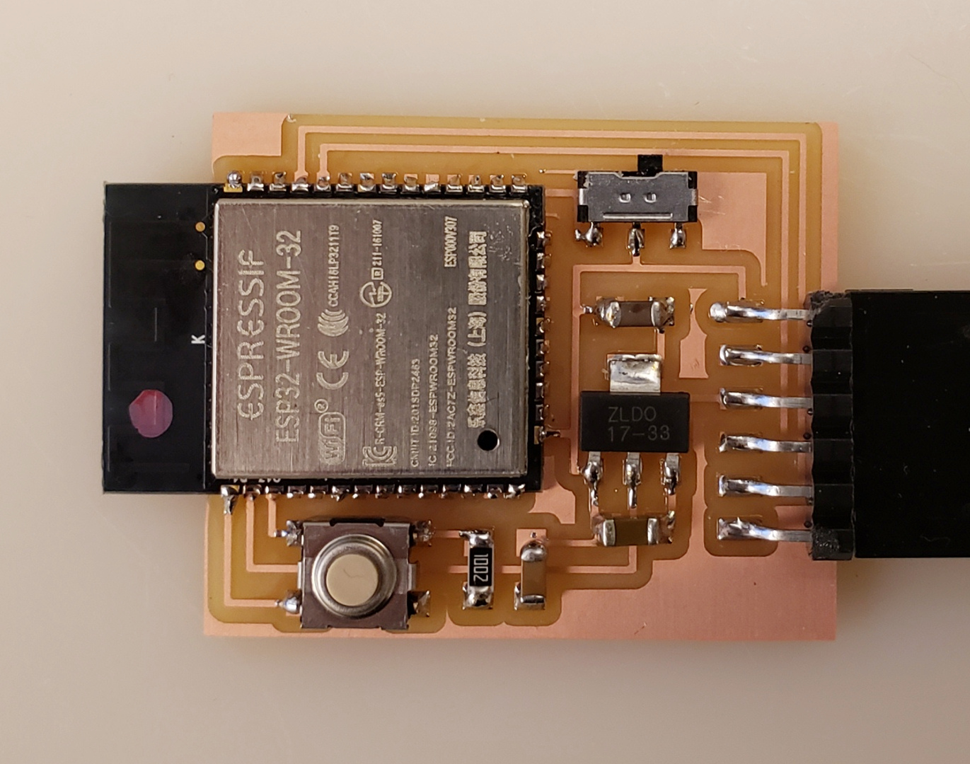
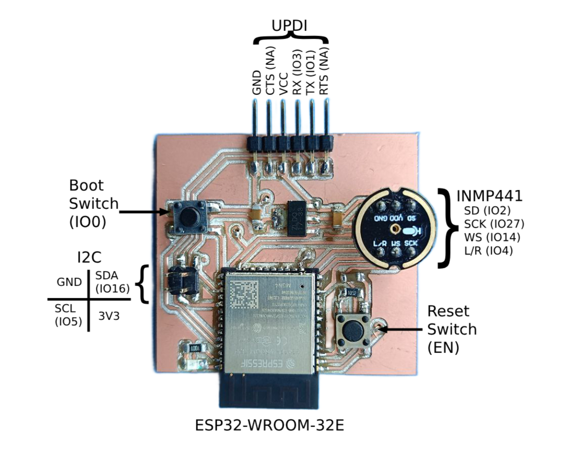
I went through Neil's assembled board and the PCB circuit to understand how the Reset buttonand the Boot button were designed and applied it to my design. Since GPIO 0 controls the boot mode and is also responsible for sending signals to the clok pin for INMP441, they share a common IO pin.
Adding an I2S connection
I got the pinout digram for the module
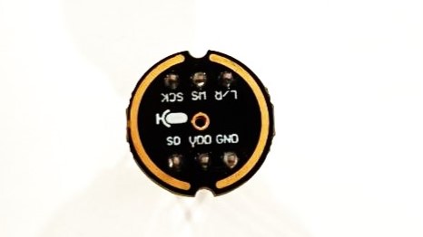
I will be drilling holes and soldering the module as a through hole component. We have two options for holes for pin headers for the module: 1 or 1.4 mm. I chose the 1 mm diameter option since the pins themselves are 0.7mm in thickness when I measured with my vernier calliper
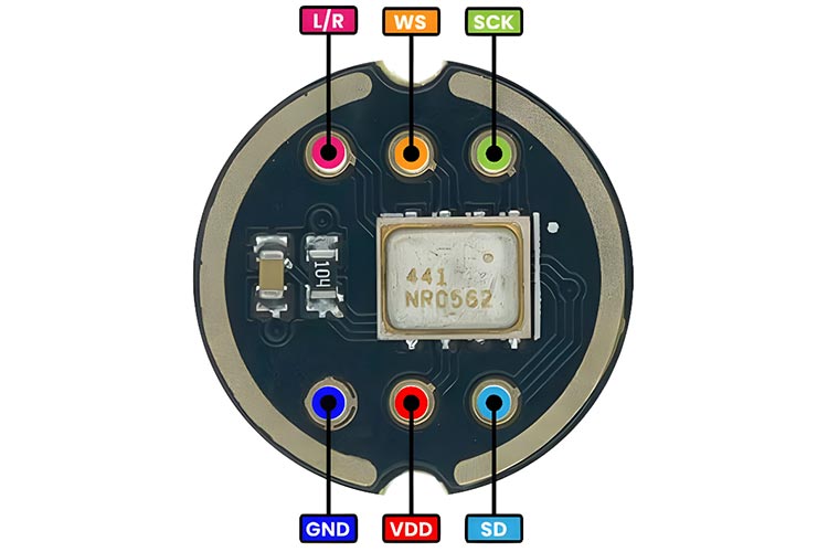
This is how my pin connections look like for the module
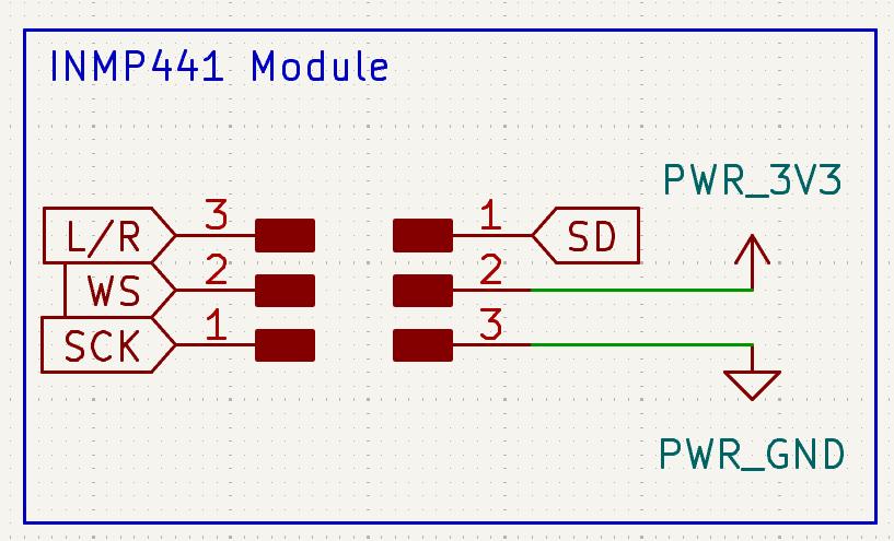
All the I2S connections can be connected to any GPIO pins, except the I2S0_CLK clock pin, which should be connected to GPIO0. The SCK is the Serial-Data Clock for the I2S interface, so I will be connecting to GPIO 0, and the rest to random GPIO pins
While making the connections I had a question about the difference SD and SDA pins on I2S and I2C respectively. To answer this I used ChatGPT
Prompt 1: Difference between I2S and I2C..
What is the difference between I²S and I²C?
Here’s a detailed comparison between I²S and I²C:
Difference Between I²S and I²C
I²S (Inter-IC Sound)
- Purpose: Used for digital audio transmission.
- Data Transfer: Continuous, synchronized audio data.
- Communication Type: Point-to-point connection.
- Clock Signals: Requires three main lines:
- Bit Clock (BCLK)
- Word Select (WS)
- Data Line (SD)
- Speed: High-speed audio data transfer.
- Applications: Used in DACs, ADCs, and audio codecs.
I²C (Inter-Integrated Circuit)
- Purpose: General-purpose communication between peripherals.
- Data Transfer: Byte-based with master-slave configuration.
- Communication Type: Multi-device bus.
- Clock Signals: Uses two lines:
- Serial Data Line (SDA)
- Serial Clock Line (SCL)
- Speed: Typically lower than I²S (up to 1 MHz).
- Applications: Used in sensors, EEPROMs, and RTCs.
Key Differences
| Feature | I²S | I²C |
|---|---|---|
| Purpose | Digital audio transmission | General-purpose peripheral communication |
| Topology | Point-to-point | Multi-device bus |
| Clock Signals | BCLK, WS, SD | SCL, SDA |
| Speed | High (MHz range) | Low (up to 1 MHz) |
| Use Cases | Audio codecs, DACs, ADCs | Sensors, EEPROMs, RTCs |
Prompt 2: Do we need separate pin connections for SDA and SD?..
Do we need separate pin connections for SDA (I2C) and SD (I2S)?
Separate Pin Requirements for SDA and SD
Yes! They serve different purposes and must be wired separately.
| Feature | I²C (SDA) | I²S (SD) |
|---|---|---|
| Pin Name | SDA (Serial Data) | SD / SDATA (Serial Data for I²S) |
| Function | Bidirectional data communication | Transmits audio data in one direction |
| Clock Signal Used | SCL (Serial Clock) | BCLK (Bit Clock) and WS (Word Select) |
| Bus Type | Shared bus (multiple devices on SDA) | Dedicated connection between transmitter and receiver |
| Pull-up Resistors Needed? | Yes (typically 4.7kΩ or 10kΩ) | No (driven by master device) |
| Data Format | Byte-based with start/stop bits | Continuous stream of audio data |
Conclusion
You cannot share the SDA pin from I²C with the SD pin from I²S because they operate on different protocols and electrical requirements. Each must be wired separately to avoid conflicts.
Electronic Rule Checker
Then I ran the ERC and proceeded to correct any mistakes
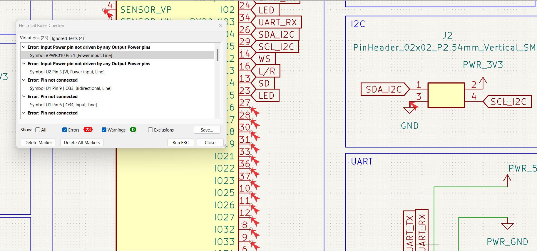
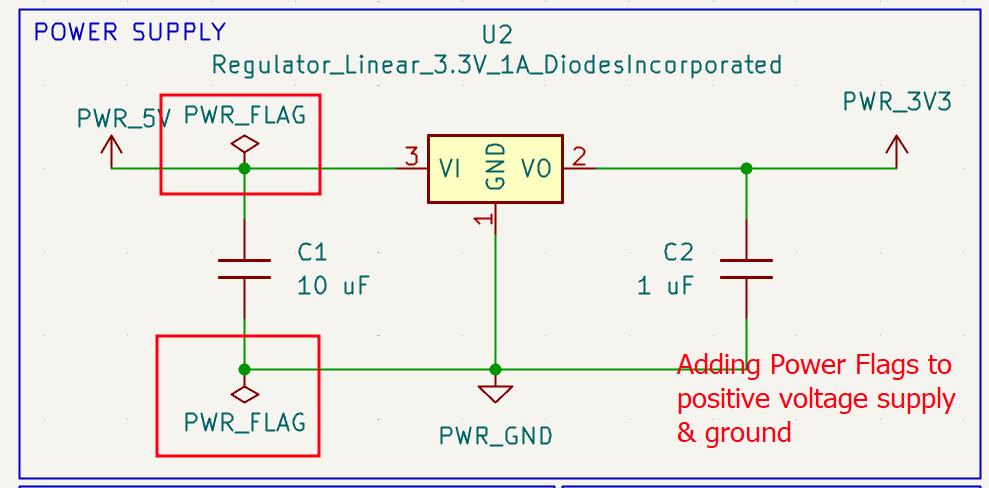
Most of my errors were solved by adding PWR FLAGS.
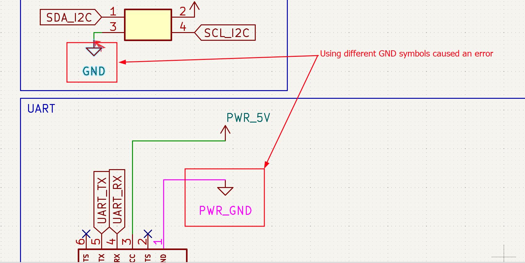
I used two different GND symbols which caused an error to show.
I got feedback from my instructor saying that I should avoid using the GPIO 0 pin to control
other modules since it should be reserved for rebooting the MCU. I realized I had just assumed
that I2S0_CLK clock pin that was mentioned in the documentation for the INMP441 is
the same as the SCK pinout observed in the module. To find out more I used ChatGPT:
Prompt 1: Are the SCK and I2S0_CLK the same pins in INMP441?..
Are the SCK and I2S0_CLK the same pins in the INMP441 microphone?
Here’s the explanation about SCK and I2S0_CLK in INMP44_
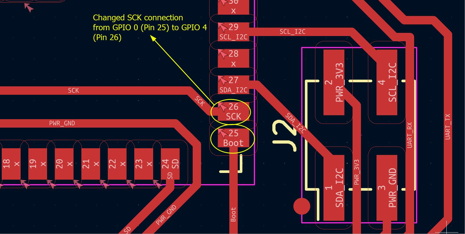
So I followed the exaample that this instructable that Revishankar (FA2025) provided that showed how an ESP32 MCU was connected to the INMP441 module, I changed SCK pin from GPIO 0 to GPIO 4
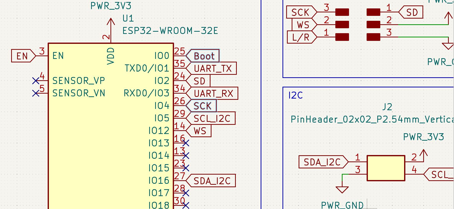
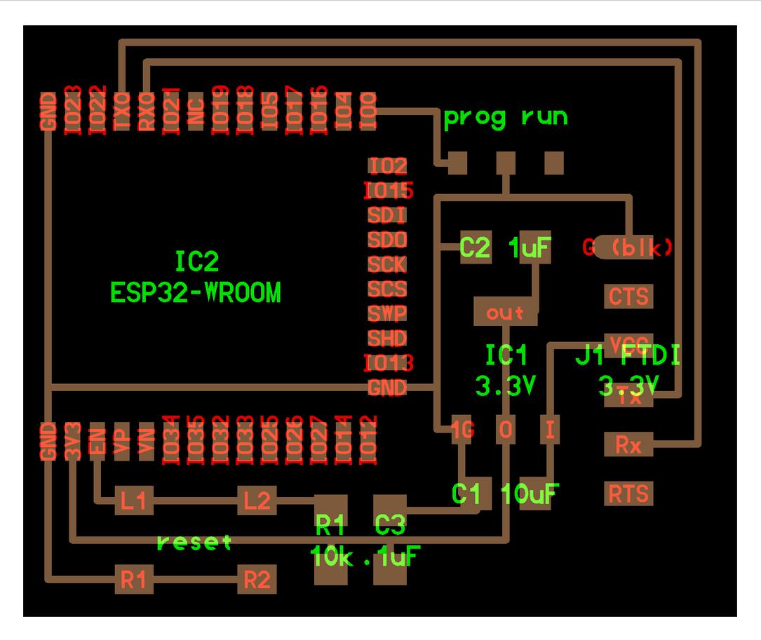
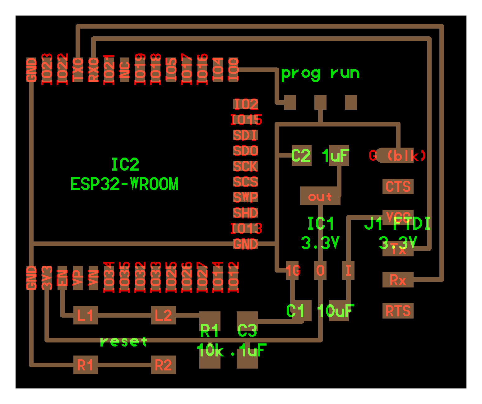
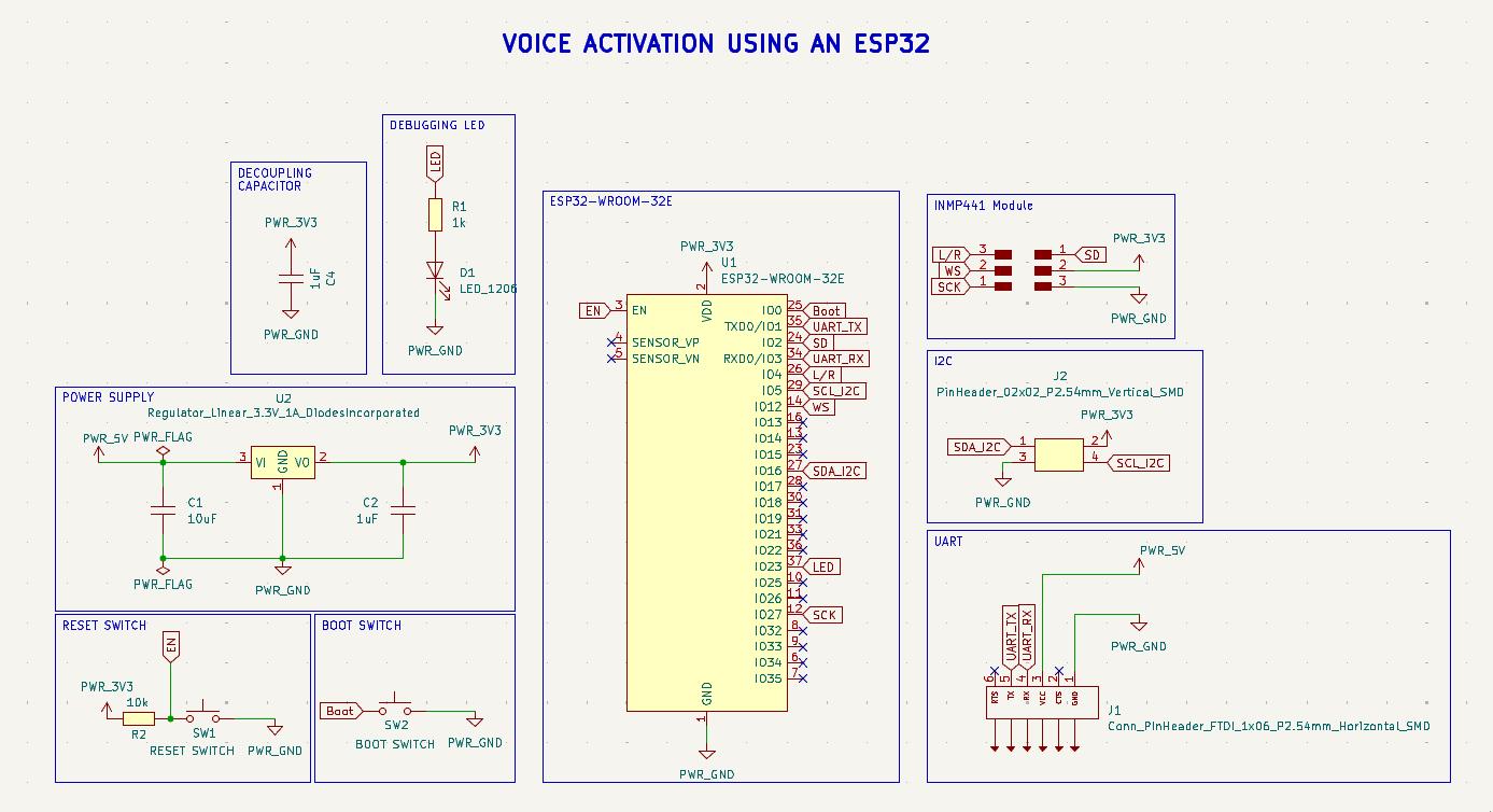
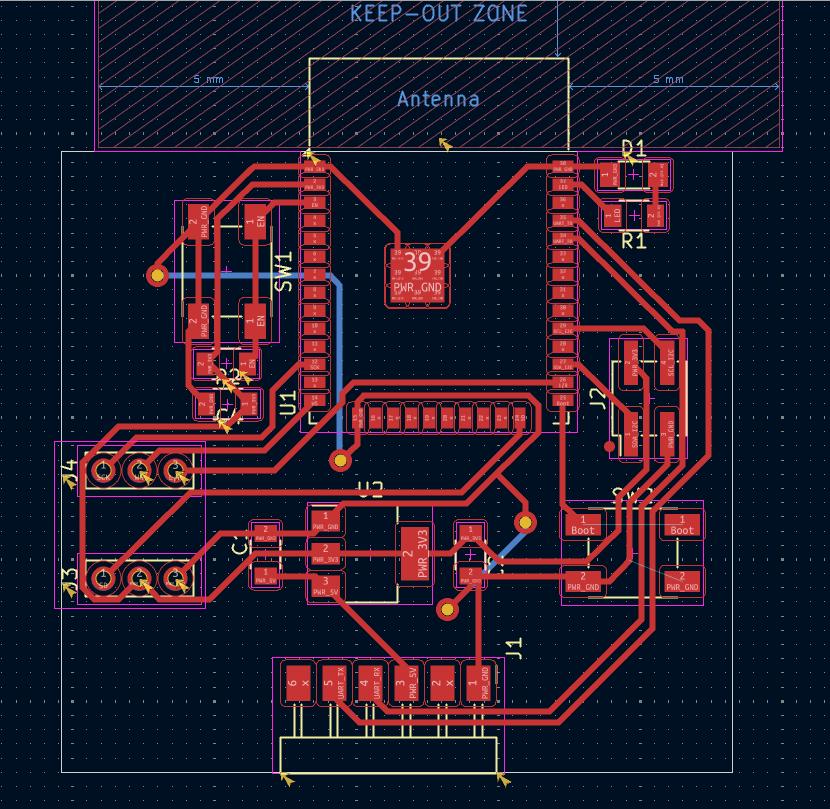
This is the completed schematic of my circuit
Adding traces
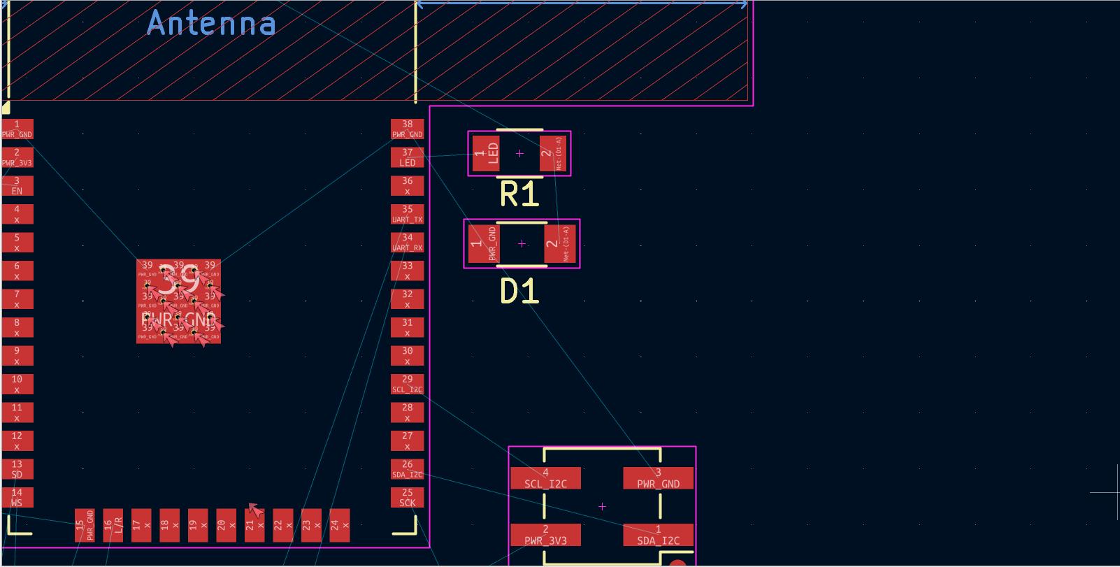
I repositioned LED connection from pin 2 to pin 37 to be able to better arrange them
Based on instructor input, I was showed how the two sets of pins are spaced at a distance equal to a gap of 4 pins, so I have arranged them as such before deleting them and grouping them together
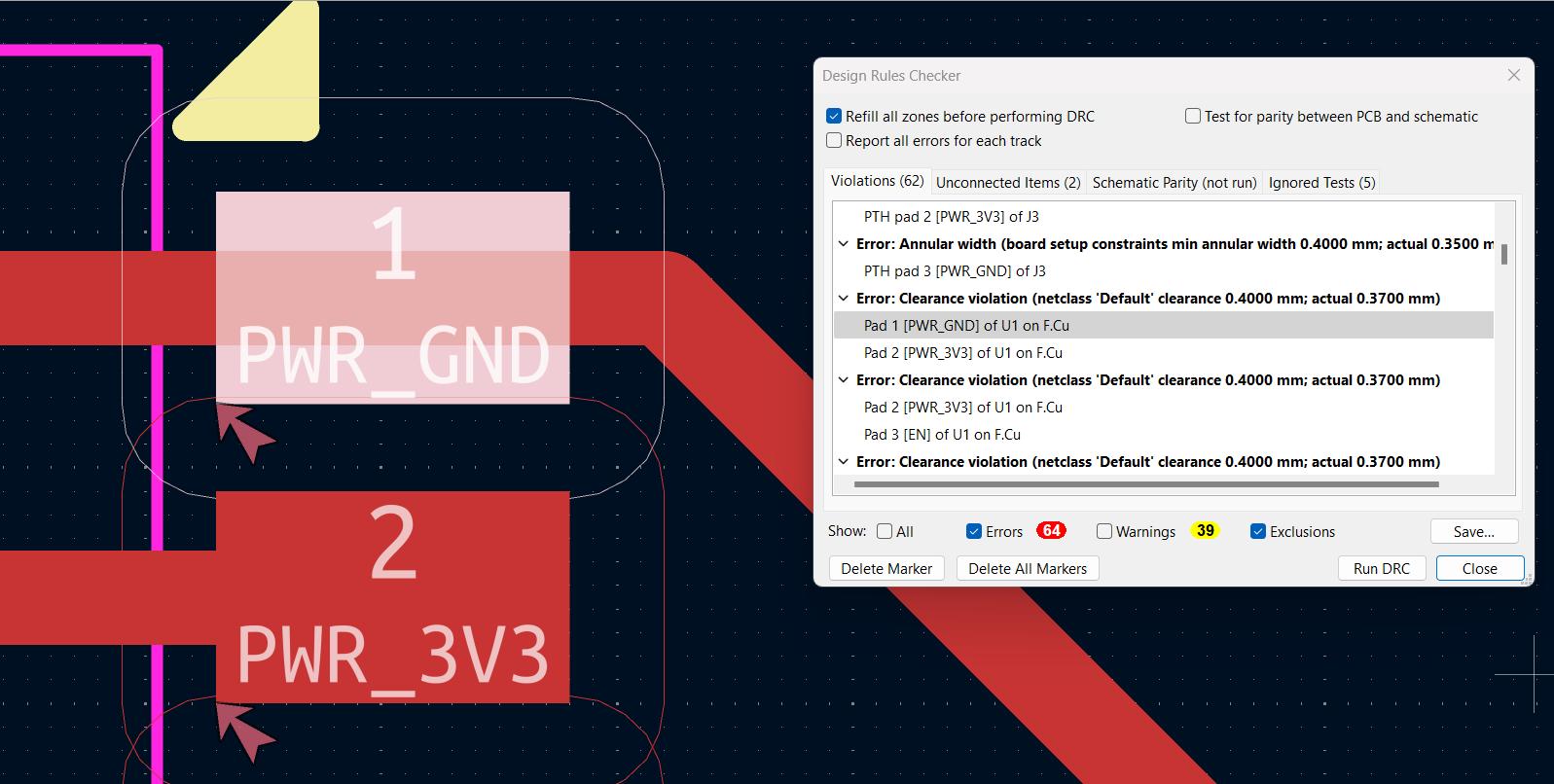
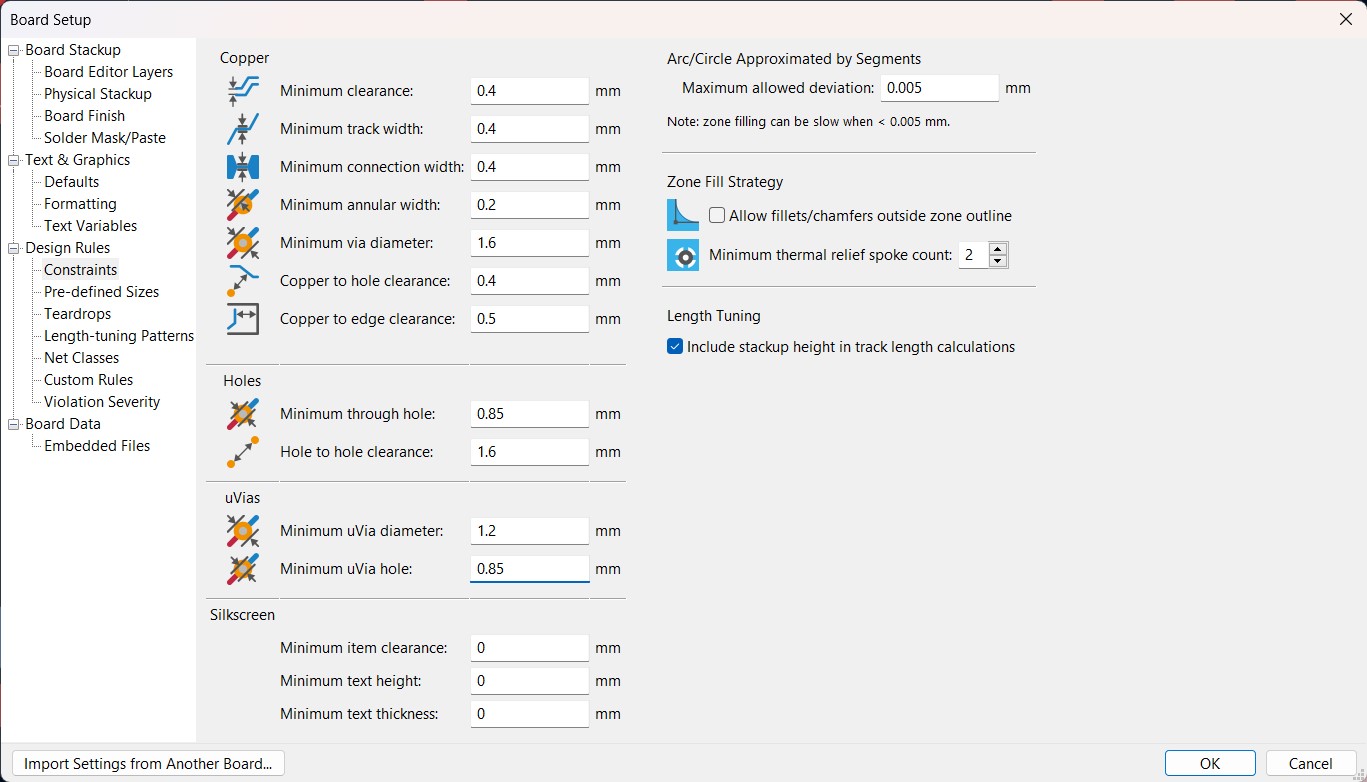
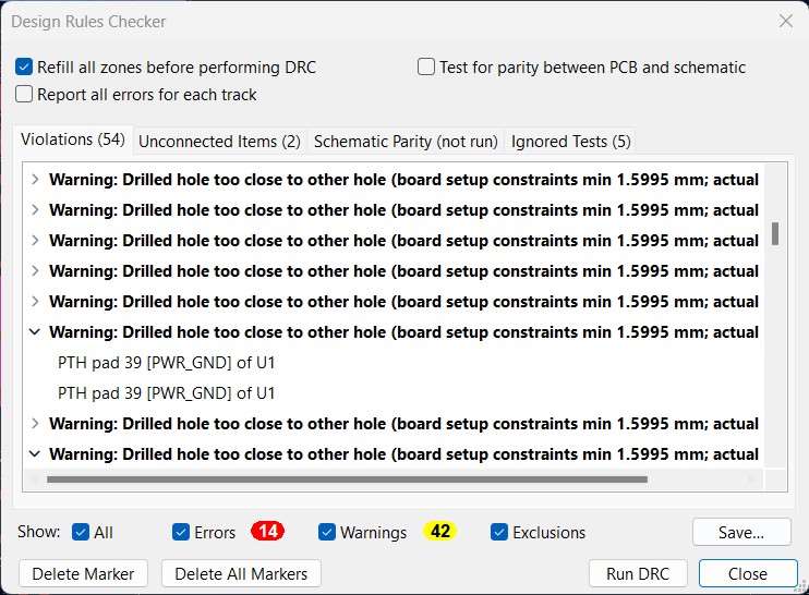
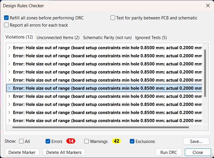
Design Rules Checker
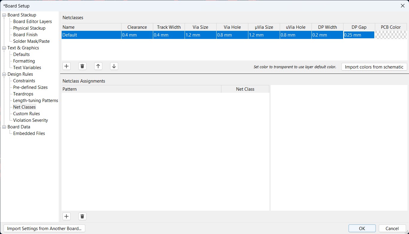
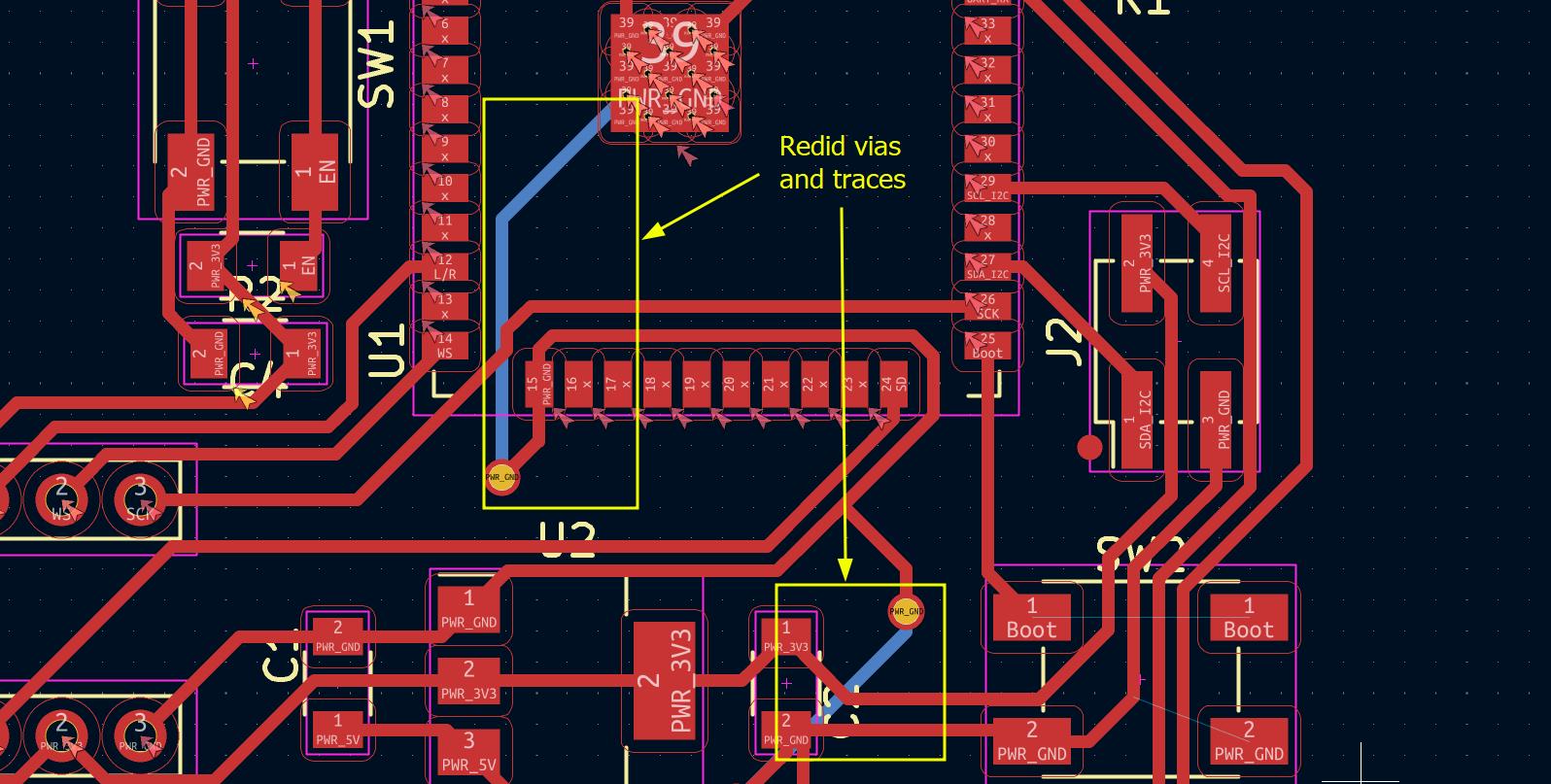
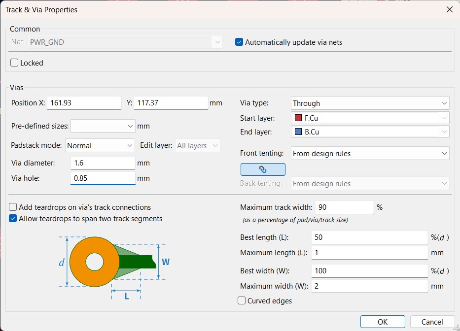
I then used the Design Rule Checker, I found errors on parameters of the vias. based on feedback from Midhun (FA2024), I realized that I did not add parameters for NetClass, so I added them now based on his parameters for our milling machine, then I redid the vias and the traces going behind the Board in B.Cu
But an error relatd to pad width appeared. I was able to solve itby reducing the width of the pad in the Y direction by 0.1mm to 0.8 mm. Then select the modified pad, right click > Push pad properties to ther pads > Change Pads on Current Footprint. Then run Design Ruless Checker again to verify that all the errors related to pad size has been reectified.
.jpg)
.jpg)
.jpg)
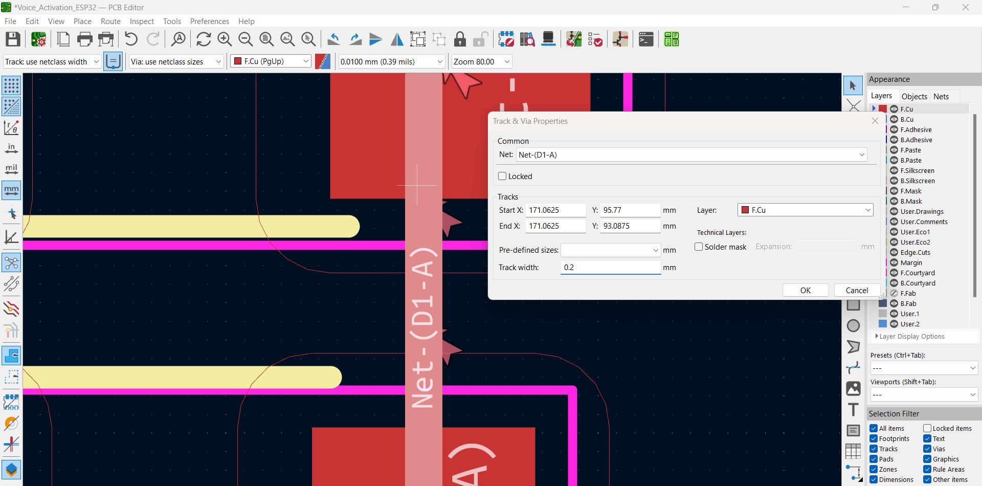
I had to do the same to the pads oriented in the footprint horizontally.did the same for errors related to pad width in the X direction by reducing width by 0.1 mm
Error 2: For some unknown reason, some of the track widths stayed 0.2 mm so I had to manually change them
Error 3: Annular width errors of pin headers were corrected by reducing .
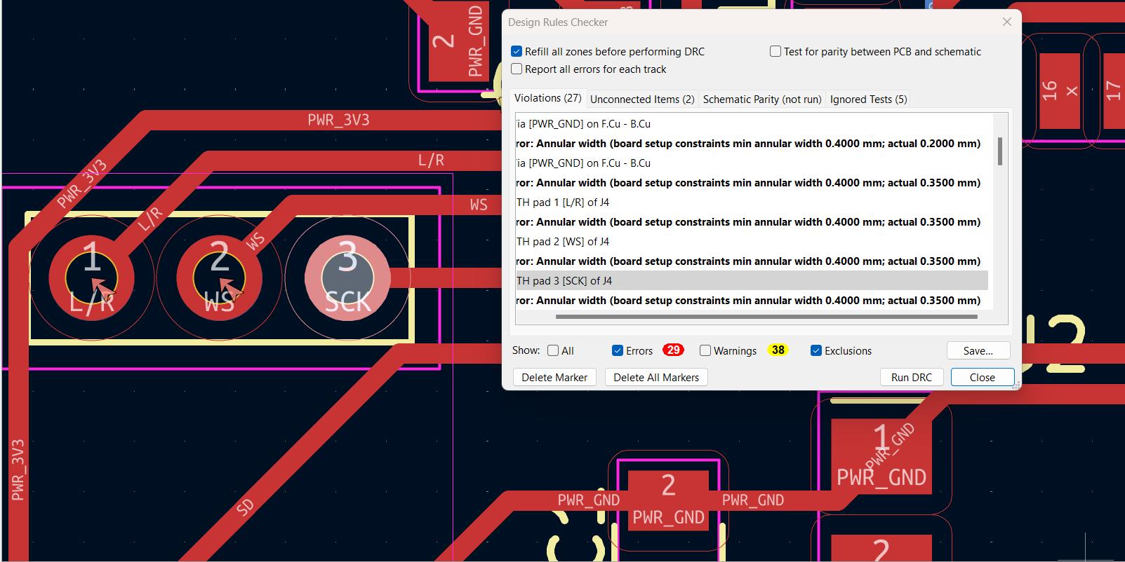
Error 4: Errors related to via holes were corrected by adjusting the hole diameter to 0.85, and diamater to 1.6, which is the minimum required hole size for rivets based on experiments. Then I manually changed all of the hole dimensions
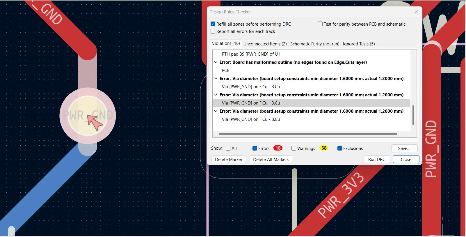
All these warnings and errors are related to pins on the bottom of the ESP32 chip that I wont be connecting so I can ignore all of them
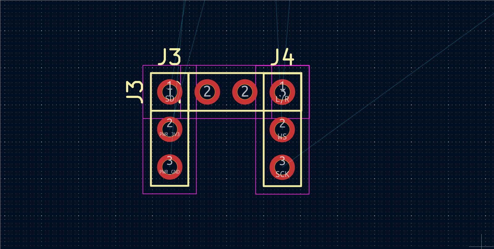
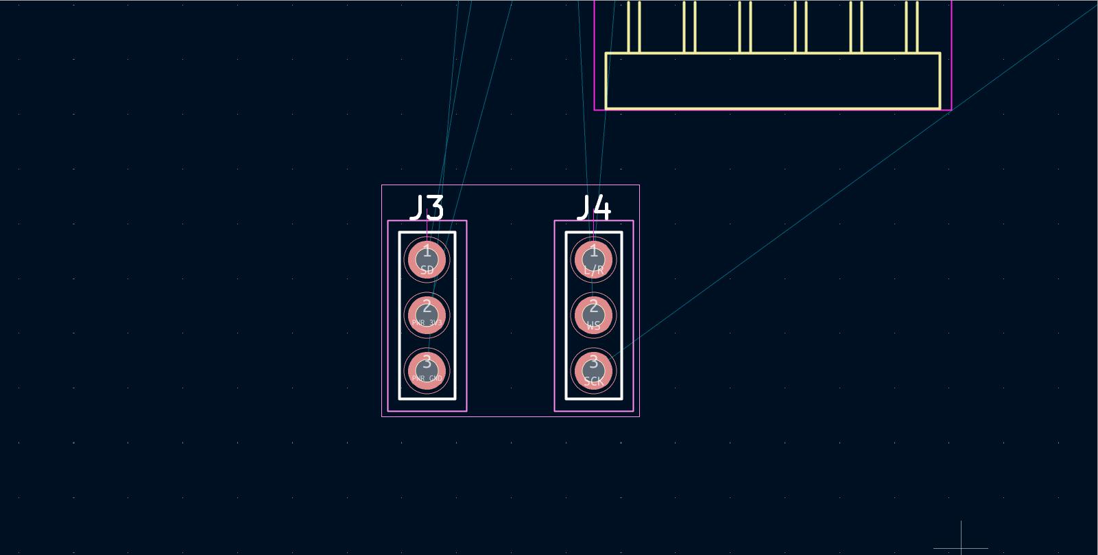
When checking my design, my instructor pointed out that I had connected the I2S connections in such a way that the module would have to be set upside down, so I took a photo of the module in the correct orientation and connected them again, changing the changing the position of L/R and SCK and the pin connections with each other
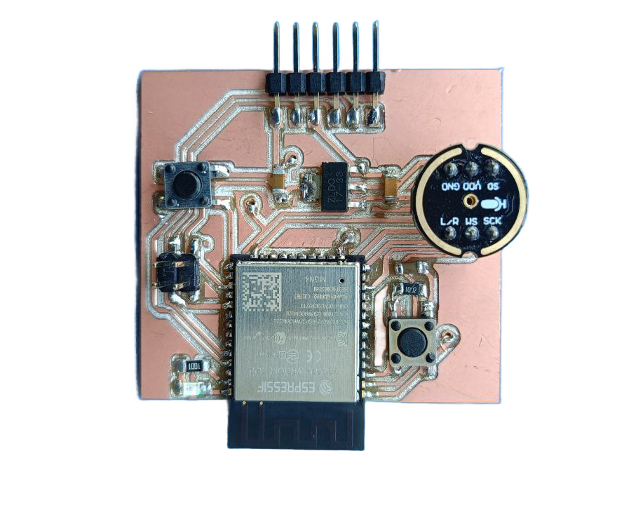
This is my final PCB design
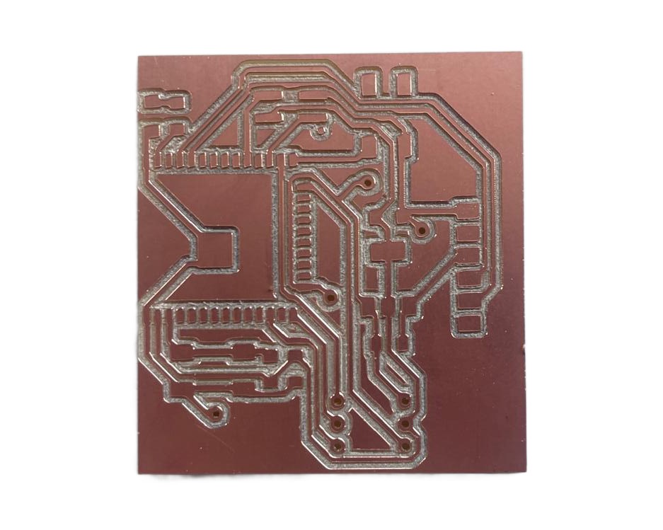
Milling
Now its time to mill my design. Just like before I use the 0.2 mm V bit for making the traces and 1/32" flat end mill to cut the PCB
Soldering
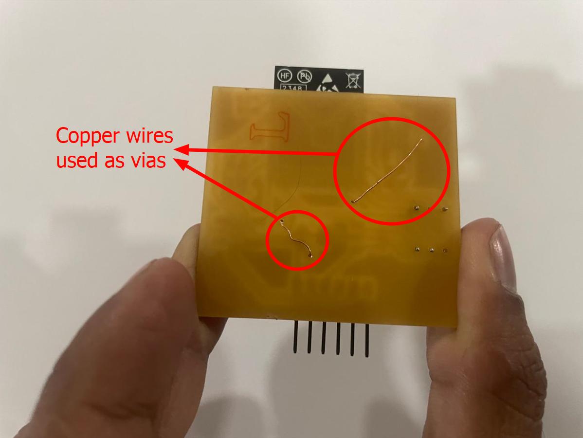
I also added wires behind the board to connect between two holes
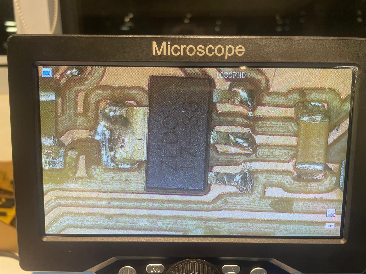
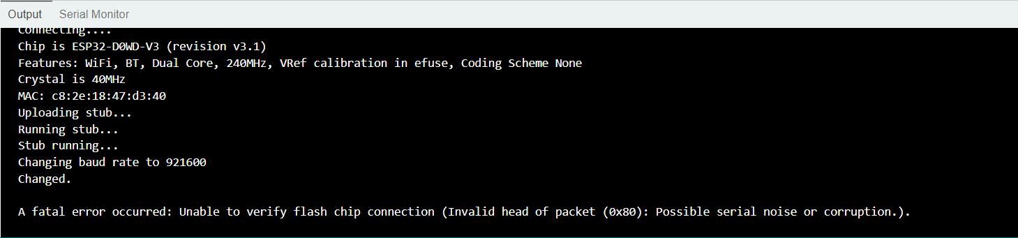
Error: Tried desoldering the MEMS mic module using a heat gun, ended up removing all the components, a tiny MIC and capacitor and resistor
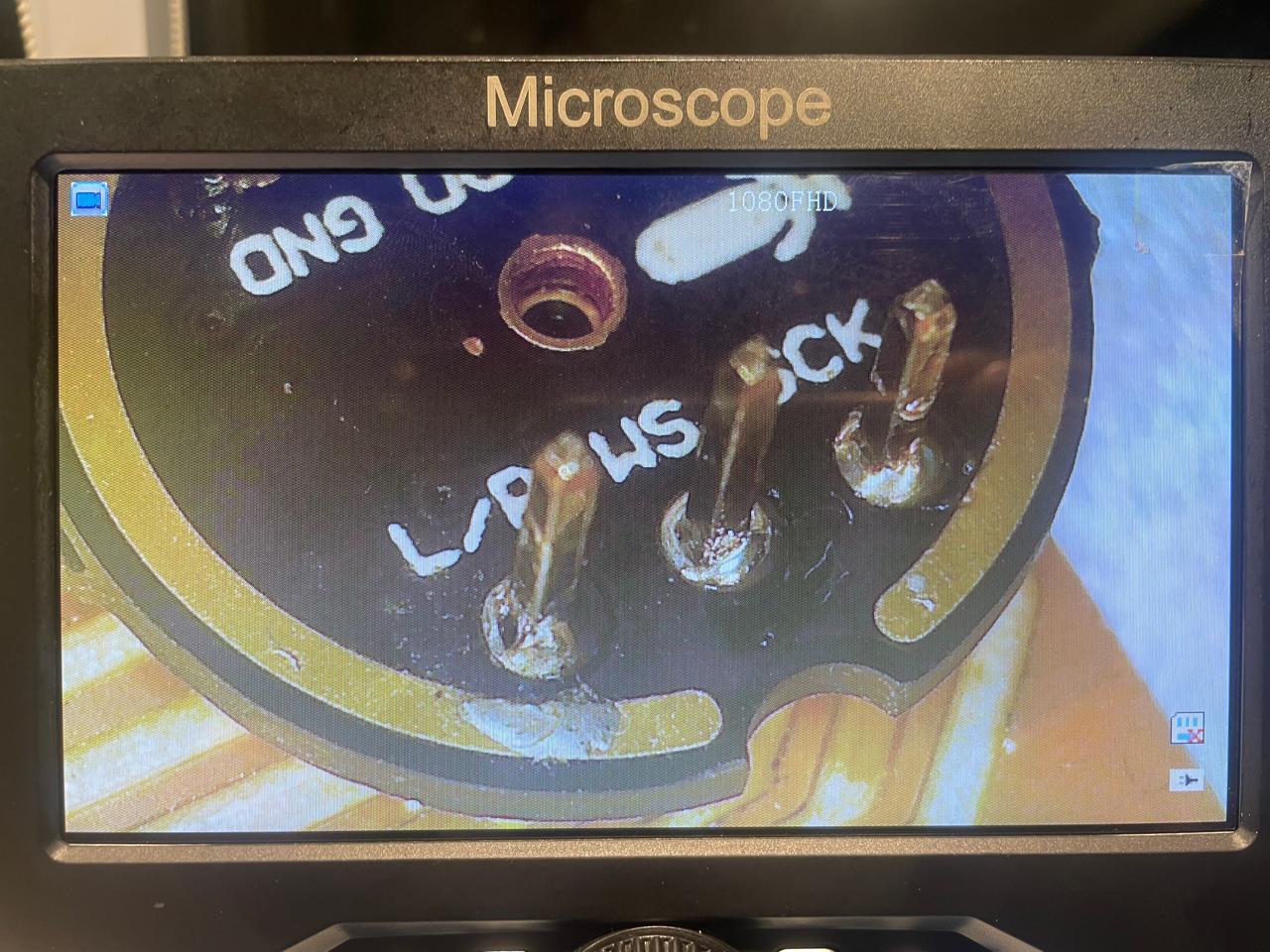
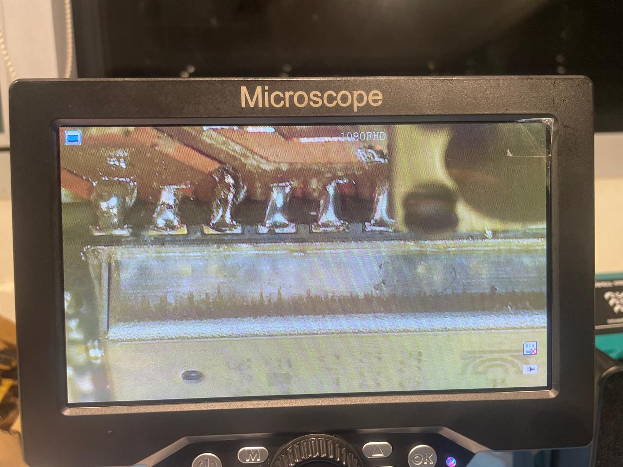
Verification
testing on microscope
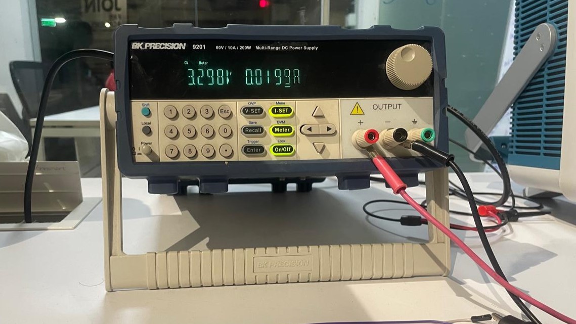
Testing on oscilloscope: No constant current draw, current draw is less than prev set limit of 0.1 A (around 0.02A or 20 mA)
Programming
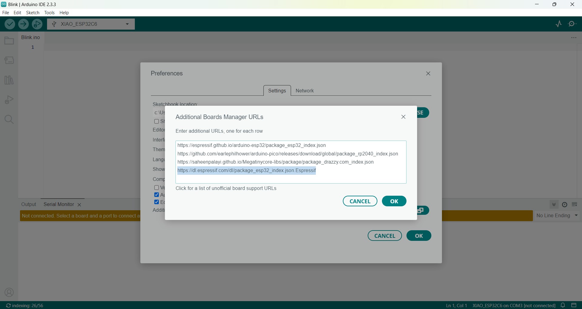
To be able to set the ESP32 with Arduino IDE, i used the help of ChatGPT
Prompt: How to set up ESP32 for Arduino IDE?
How do I set up an ESP32 board to work with the Arduino IDE?
Here's a step-by-step guide to setting up ESP32 for Arduino IDE:
Step 1: Install Arduino IDE
Download and install the latest version of Arduino IDE.
Step 2: Install ESP32 Board in Arduino IDE
- Open Arduino IDE.
- Go to File > Preferences (Windows) or Arduino > Preferences (Mac).
- In "Additional Board Manager URLs", add:
https://raw.githubusercontent.com/espressif/arduino-esp32/gh-pages/package_esp32_index.jsonClick OK and close Preferences.
Step 3: Install ESP32 Board Package
- Go to Tools > Board > Boards Manager.
- Search for "ESP32".
- Install "esp32 by Espressif Systems".
Step 4: Install USB-to-Serial Drivers (If Needed)
Step 5: Select the ESP32 Board
- Go to Tools > Board and select "ESP32 Dev Module".
- Go to Tools > Port and select the ESP32's port.
Step 6: Test with a Simple Sketch
Upload the following Blink sketch:
void setup() {
    pinMode(2, OUTPUT); // GPIO 2 is usually the built-in LED
}

void loop() {
    digitalWrite(2, HIGH);
    delay(1000);
    digitalWrite(2, LOW);
    delay(1000);
}
Click "Upload" and press the BOOT button if needed.
Step 7: Open Serial Monitor
- Go to Tools > Serial Monitor.
- Set baud rate to 115200.
- Verify the Blink program is running.
✅ You're now ready to develop projects with ESP32 on Arduino IDE! 🚀
The setup was pretty simple, simply install the board manager using the following URL:
https://raw.githubusercontent.com/espressif/arduino-esp32/gh-pages/package_esp32_index.json
and select the board and port
Note: When you upload the code, when you see the 'Connecting' message, keep pressing the Boot button and press the Reset button once. One you see the message 'Leaving' you press the 'Reset' button once more to start the program, and the program will start running.
Blink Program to verify that the board works
I now used the Blink program to test the proper functioning of the board. But the program did not work. My instructor helped identify the following errors
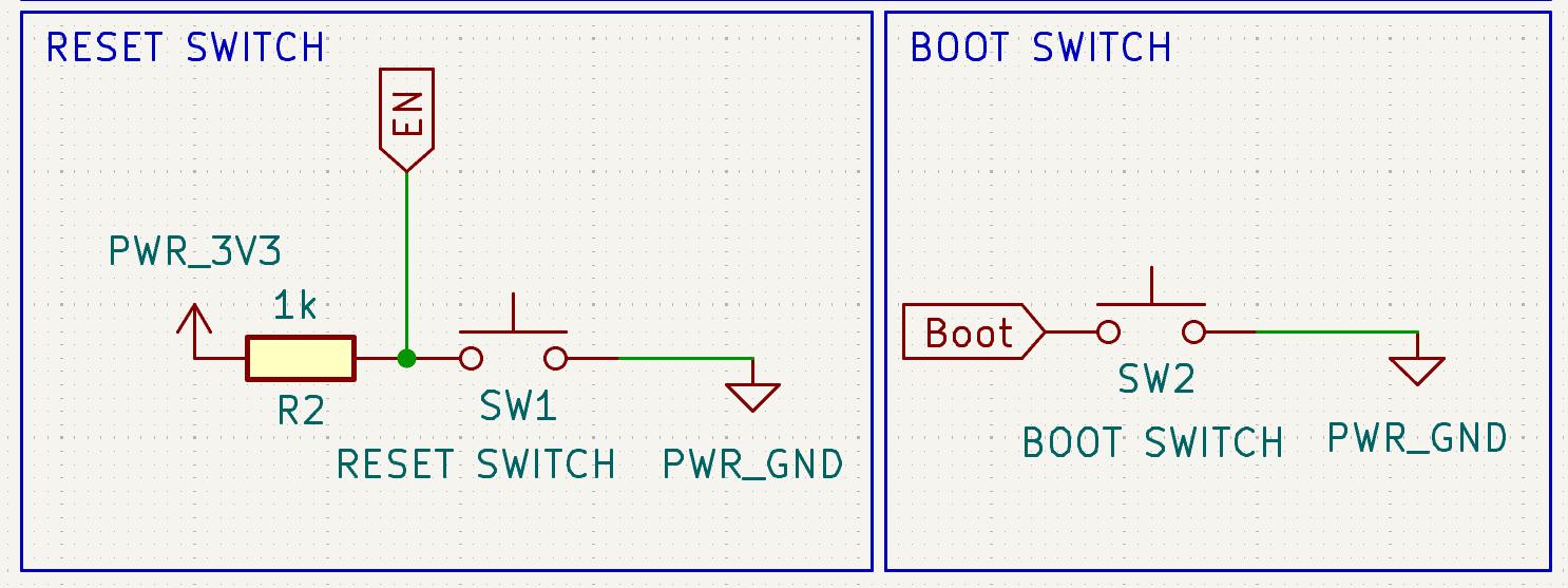
Error 1: I used a 1k instead of 10k value for the resistor connected in series to the Reset Switch
Error 2: I had shorted the tx and rx connections while soldering
Error 3: I used the wrong pin for LED, should have been IO23
                                void setup() {
                                    pinMode(23, OUTPUT); // GPIO 2 is usually the built-in LED
                                }

                                void loop() {
                                    digitalWrite(23, HIGH);
                                    delay(1000);
                                    digitalWrite(23, LOW);
                                    delay(1000);
                                }
Sample code borrowed from Revishankar (FA25) Code not working with INMP441, maybe because of previous unintented disassembly of components
Error: Serial Monitor howed an error and serial plotter showed continuous lines with no variation. Was solved when sliding the switch in my programmer board
When I ran the code again I faced this error
turns out it was due to me not inputting the right pin numbers for SCL, SD, WS
Now I wanted to make the on-board LED to light up if the noise captured by microphone increases above 1000
Error: I also faced errors with While loops. Taking out the digitalWrite statement also did not work
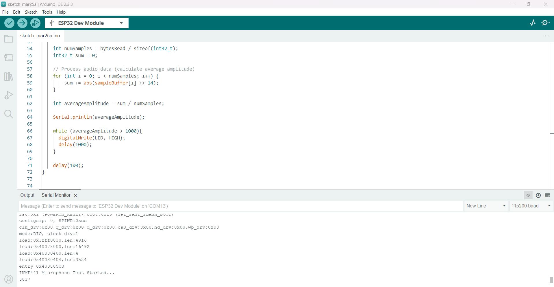
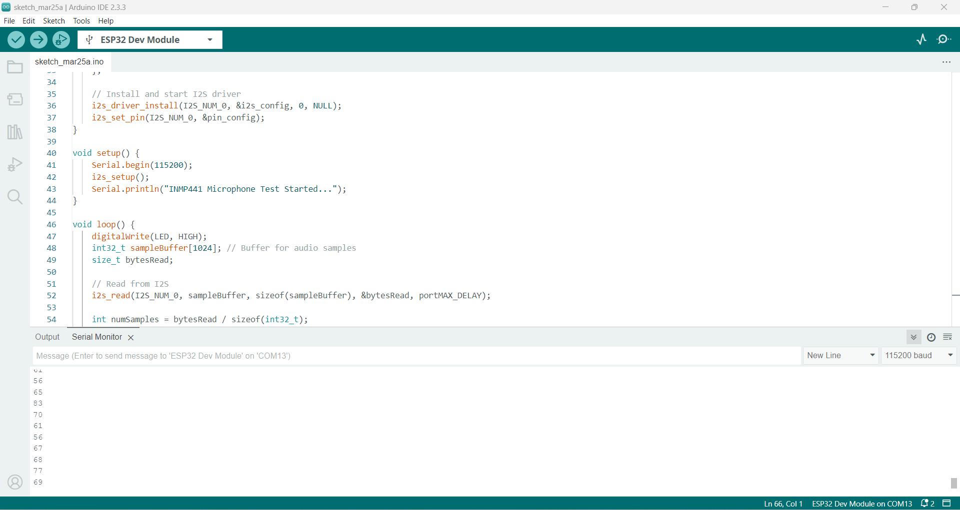
This was solved by adding the pinMode statement in void setup
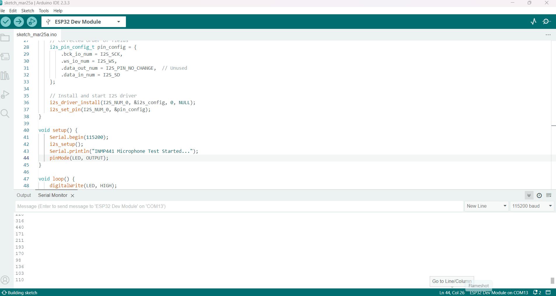
    #include <Arduino.h>
    #include <driver/i2s.h>

    #define I2S_WS  12
    #define I2S_SCK 27
    #define I2S_SD  2
    #define LED 23

    void i2s_setup() {
        i2s_config_t i2s_config = {
            .mode = (i2s_mode_t)(I2S_MODE_MASTER | I2S_MODE_RX),
            .sample_rate = 16000,
            .bits_per_sample = I2S_BITS_PER_SAMPLE_32BIT,
            .channel_format = I2S_CHANNEL_FMT_ONLY_LEFT,
            .communication_format = I2S_COMM_FORMAT_I2S_MSB,
            .intr_alloc_flags = ESP_INTR_FLAG_LEVEL1,
            .dma_buf_count = 8,
            .dma_buf_len = 1024,
            .use_apll = false,
            .tx_desc_auto_clear = false,
            .fixed_mclk = 0
        };

        i2s_pin_config_t pin_config = {
            .bck_io_num = I2S_SCK,
            .ws_io_num = I2S_WS,
            .data_out_num = I2S_PIN_NO_CHANGE,
            .data_in_num = I2S_SD
        };

        i2s_driver_install(I2S_NUM_0, &i2s_config, 0, NULL);
        i2s_set_pin(I2S_NUM_0, &pin_config);
    }

    void setup() {
        Serial.begin(115200);
        i2s_setup();
        Serial.println("INMP441 Microphone Test Started...");
        pinMode(LED, OUTPUT);
    }

    void loop() {
        int32_t sampleBuffer[1024];
        size_t bytesRead;

        i2s_read(I2S_NUM_0, sampleBuffer, sizeof(sampleBuffer), &bytesRead, portMAX_DELAY);

        int numSamples = bytesRead / sizeof(int32_t);
        int32_t sum = 0;

        for (int i = 0; i < numSamples; i++) {
            sum += abs(sampleBuffer[i] >> 14);
        }

        int averageAmplitude = sum / numSamples;

        if (averageAmplitude>900){
            digitalWrite (LED, HIGH);
            delay(500);
        }
        else{
            digitalWrite(LED, LOW);
        }


        // Serial.print("Amplitude: ");
        Serial.println(averageAmplitude);

        delay(100);
    }
Now to add voice commands I use this youtube video
Once you clone both repos, To open a folder in VS Code folder, go to the file
directory and type
code .
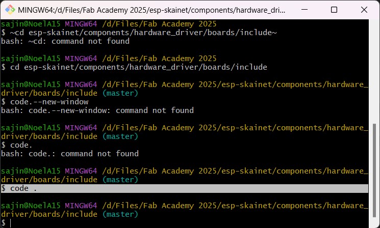
But I was unable to access the required file, so I used Chat GPT
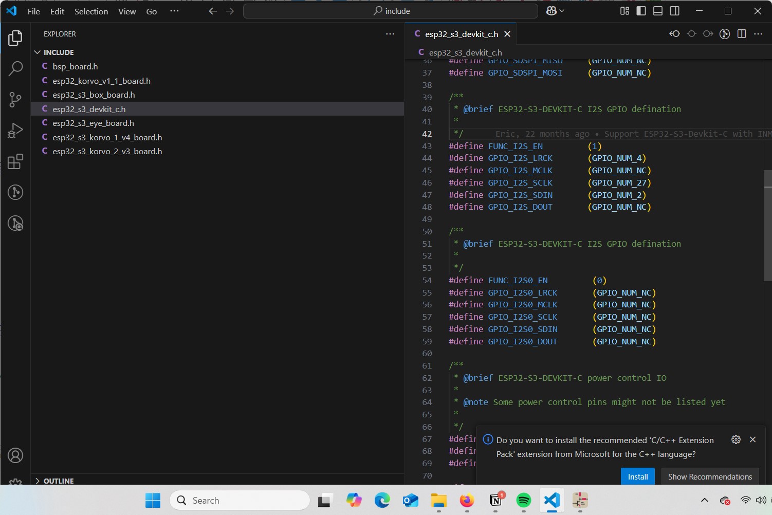
Prompt 1 : Why is 'esp32_s3_devkit_c.h' folder missing?
Quick Start with ESP-Skainet for Generic ESP32-S3 DevKit-C

Pre-requisite:
Now this project runs on IDF version 5.x.

ESP-Skainet:
Make sure you have cloned my project branch with the '--branch'. Also, need to get all submodules so don't forget the option '--recursive'.

    git clone --branch ESP32-S3-Devkit-C --recursive git@github.com:0015/esp-skainet.git

Example that can be operated in ESP32-DevKit-C and INMP441

Set your I2S microphone settings

    cd esp-skainet/components/hardware_driver/boards/include

Open the file, 'esp32_s3_devkit_c.h'

    #define FUNC_I2S_EN (1)
    #define GPIO_I2S_LRCK (GPIO_NUM_11)
    #define GPIO_I2S_MCLK (GPIO_NUM_NC)
    #define GPIO_I2S_SCLK (GPIO_NUM_12)
    #define GPIO_I2S_SDIN (GPIO_NUM_10)
    #define GPIO_I2S_DOUT (GPIO_NUM_NC)
Possible Reasons & Solutions
1. Repository Not Cloned Properly
Ensure you used the correct branch and included submodules during cloning:
git clone --branch ESP32-S3-Devkit-C --recursive git@github.com:0015/esp-skainet.git
If you forgot --recursive, update submodules manually:
cd esp-skainet
git submodule update --init --recursive
2. File or Directory is Missing in the Repository
Navigate to the include directory and check if the file exists:
ls esp-skainet/components/hardware_driver/boards/include/
3. Wrong Branch or Version
Verify that you are on the correct branch:
git branch
If incorrect, switch to the correct branch:
git checkout ESP32-S3-Devkit-C
git pull origin ESP32-S3-Devkit-C
4. Corrupt or Incomplete Clone
If the file is still missing, try recloning the repository:
rm -rf esp-skainet
git clone --branch ESP32-S3-Devkit-C --recursive git@github.com:0015/esp-skainet.git
5. File Might Have Been Renamed or Moved
Check the repository history for changes:
git log -- components/hardware_driver/boards/include/
If it was renamed, update your code accordingly.
If you still have trouble, check the repository’s Issues section or contact the repository maintainer.
So the solution that worked for us, was the following:
                    git branch
                    git checkout ESP32-S3-Devkit-C
                    cd esp-skainet
                    git submodule update --init --recursive
Modified .h file as such
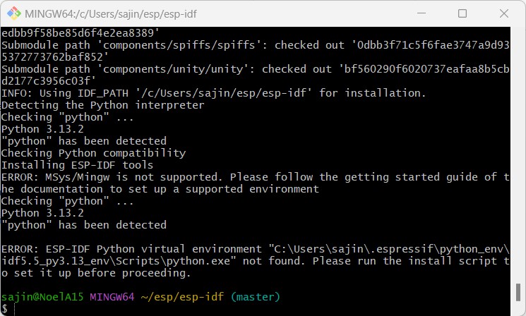
But this error showed
Conclusion
This week we:
- Used the oscilloscope to visualize the analog and digital signals of some input devices.
- Learnt to designed and mill a PCB using a ESP 32 MCU and INMP441 MEMS microphone.
- Learnt to use copper wires as vias.
- Learnt to visualize audio signals through the INMP441.
Mistakes and Solutions
- PWR Flags in KiCAD: Always add PWR flags to both PWR and GND connections in the schematic editor
- PWR and GND symbols in KiCAD: Make sure to use the the same symbol for GND and PWR everywhere
- SCK vs I2S0_CLK: The I2S0_CLK is a master clock (MCLK) for audio devices that synchronises different child clocks connected to it.It should be connected to GPIO 0 on the ESP32-WROOM-32E MCU. But the INMP441 does not have it. Instead, it has pinout for SCK, which is the I2S Bit Clock. This pin can be connected to any of the GPIO pins.
- Tips while designing a custome PCB: When designing a PCB, follow this order when looking for references: Neil's documentation in Embedded Programming Week > Documentation by other Fab students > Instructables or other example PCBs> Documentation. This is to avoid wasting time trying to understand every small detail that may not be necessary.
- Via hole and outer diameter: If DRC errors related to via parameters show up, check the properties and adjust annular width and hole size
- Pad spacing: If a DRC error shows up related to insufficient spacing between pads: Double click>Reduce width in X or Y direction and hit 'Ok'> select the modified pad > right click > Select 'Push pad properties to other pads' > Select 'Change Pads on Current Footprint.'
- Trace width: Sometimes the trace widths do not match the constraints I have added previously, and so DRC shows errors related to it. Currently, the cause of this problem is unknown, and the only known solution is to manually change the trace width of each wrong trace by double clicking to reveal trace properties dialog box
- >Header pin annular widths: For the INMP441 module, that came with the header pins that had to be soldered as a through hole component, errors related to annular width can be ignored to avoid messing with the spacing
- Pin 39 Holes: In case errors due to conflicts between the hole diameter and the constraints for pin 39 on the ESP32 show up, check if you have any requirement for the holes. If not, they can simply be deleted from the footprint editor.
- Use physical over online references while checking the pinouts when possible: Confusion could arise because the actual MEMS chip and the resistor and capacitor are placed below the board, while the hole for the mic will be at the top. If we go by source found online, you could flip the connections, causing errors. If you have the component present in stock, always use that to inform your decisions about trace connections.
- NEVER use a heat gun to desolder through hole components and devices: Doing this could result in the dislodgment of tiny components, as was the case with my INMP 441. Even though we tried resoldering all the fallen components, the module did not work properly and I had to replace it.
- Cross check connections: I connected the wrong value of resistor and shorted tx and rx connections in my board, which were easily solved with the soldering iron
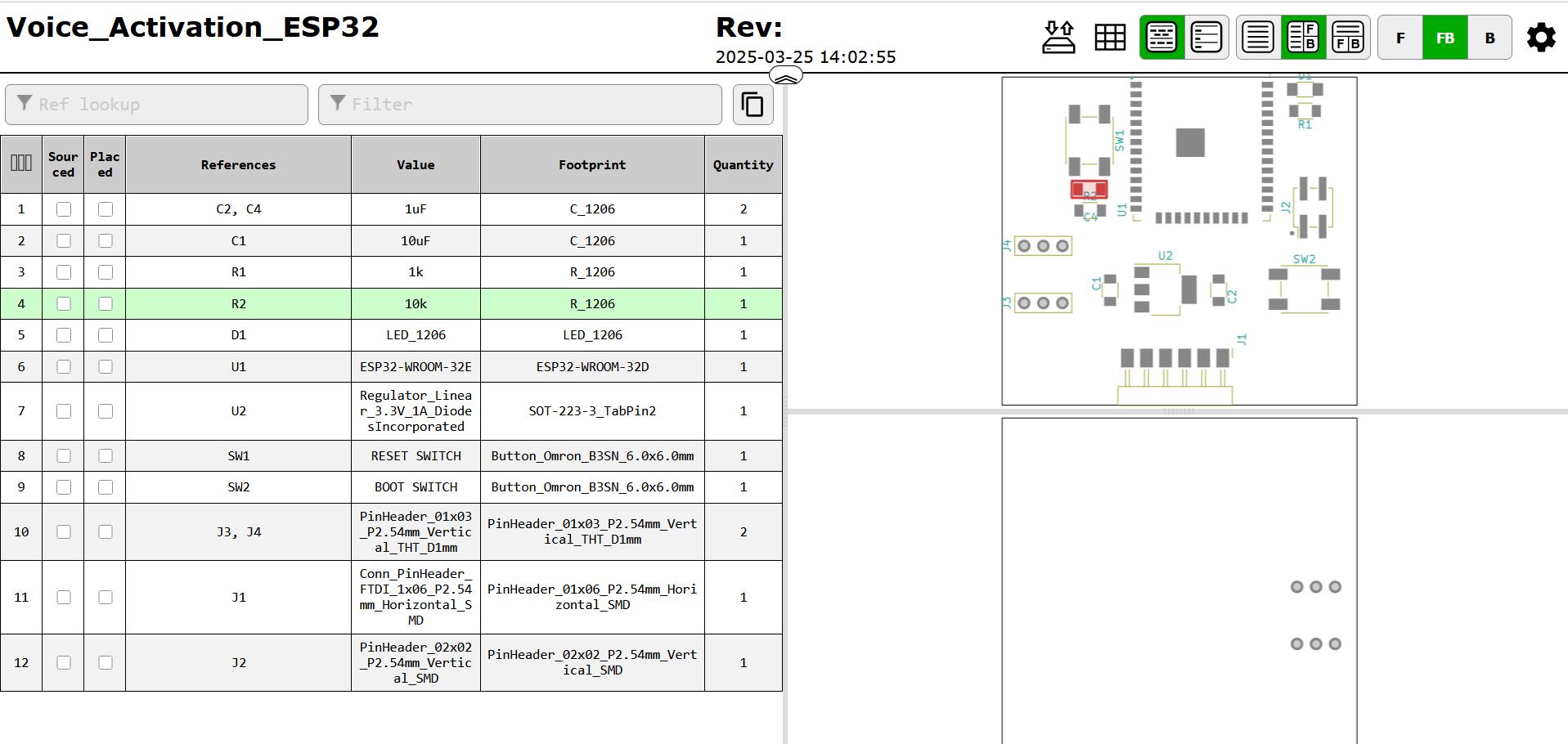
Design Files
Click here to access the design files