Week 8: Electronics Production
Objectives
These are the tasks for this week
- Group assignment:
- characterize the design rules for your in-house PCB production process
- submit a PCB design to a board house
- Individual assignment:
- make and test a microcontroller development board that you designed
- extra credit: make it with another process
Work Plan
Wednesday
- Class by Neil ✔
Thursday
- Class by Saheen ✔
- Group Assignment: Characterising PCB Design Rules on Milling machine ✔
- Documentation till Milling PCB (Individual Assignment) ✔
Friday
- Continue Documentation for Milling PCB (Individual Assignment) ✔
- Individual Assignment: Milling a PCB
- Individual Assignment: Soldering & Testing
- Complete Documentation for Individual Assignment
Saturday
- Week7: Cut peg, assemble, take photos
- Complete Documentation for Individual Assignment
- Complete Documentation for Group Assignment
Sunday
- Final project Design PCB and integrate OLED display driver
- Update in Assignment and Final Project Documentation
- Make laser cut DXF of final project
Monday
- Group Assignment: Characterising PCB Design Rules on Vinyl cutter
- Complete Documentation for Group Assignment and any pending documentation
Group Assignment
These are the design rules for tracing widths and spacings that we obtained through our group assignment.
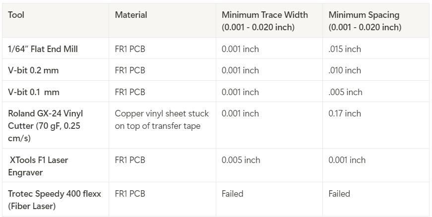
Here is the link to the group assignment
Individual Assignment
Make and test a custom development board
About the Machine
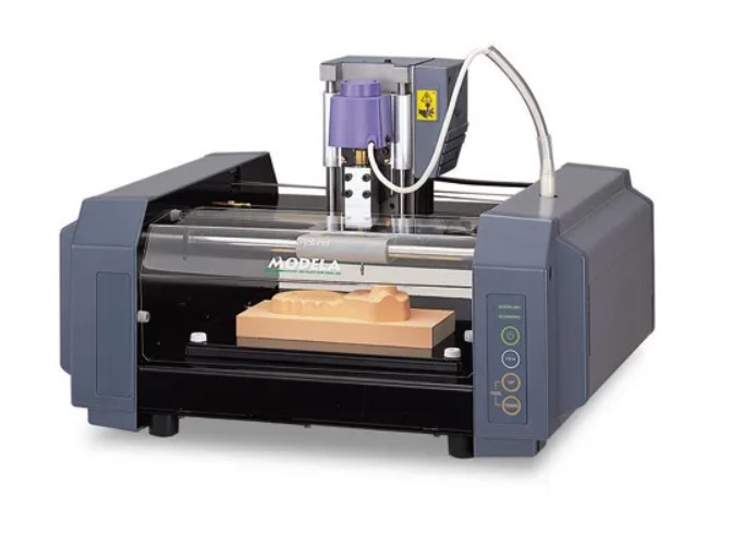
We are using the Roland MDX-20 3D Milling Machine is a compact desktop CBC milling machine that has been modified to mill PCBs with high precision in our lab.
Exporting Design Files
First I went to KiCAD and exported my design as Gerber files
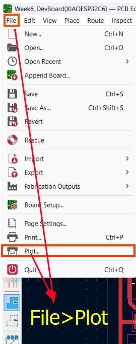
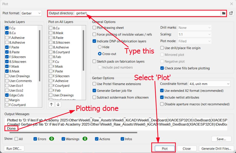
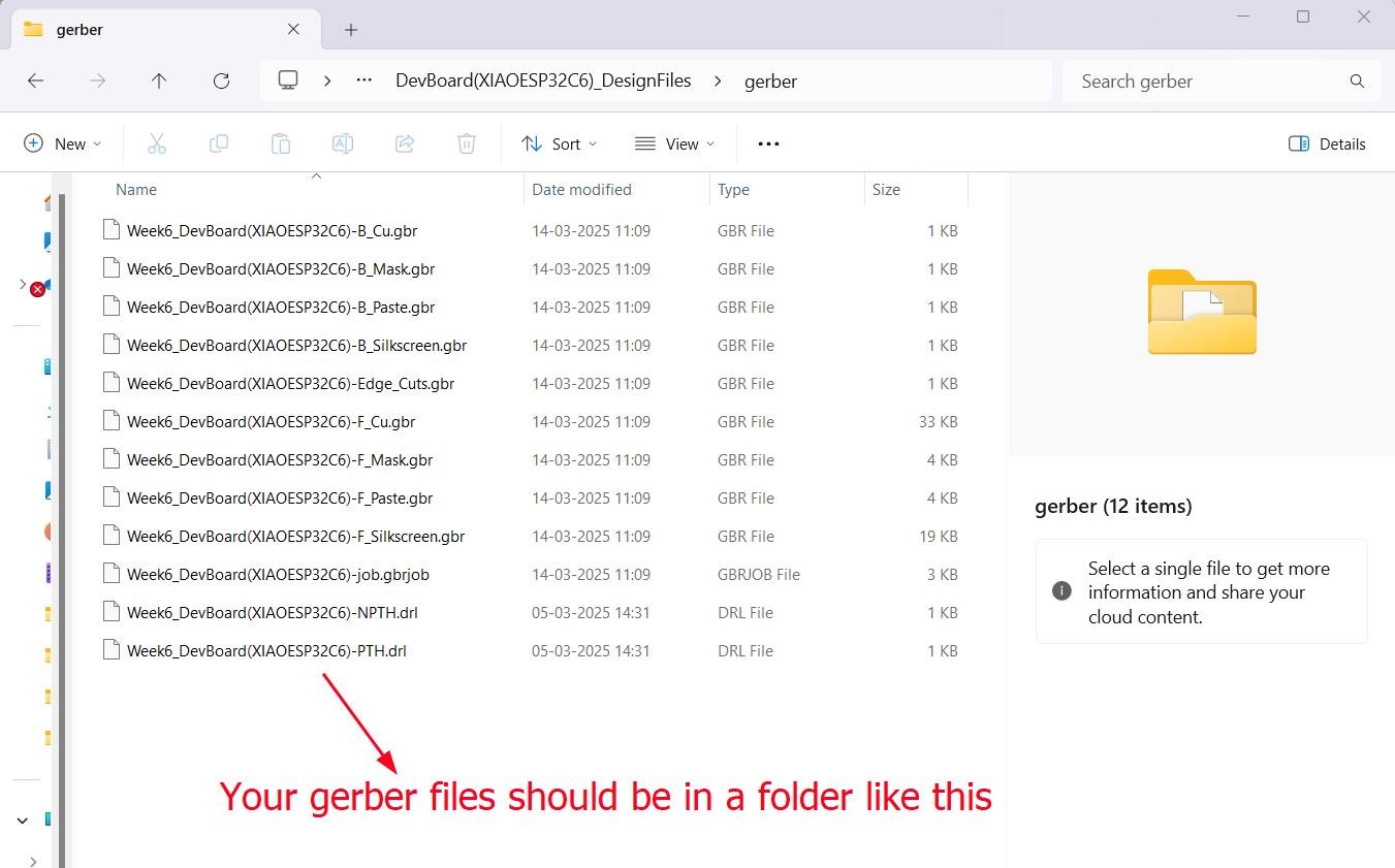
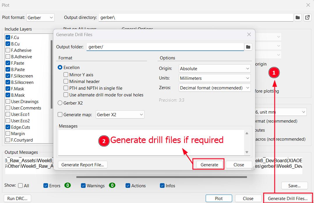
You can also generate drill files if there are holes in your design that require holes to be drilled.
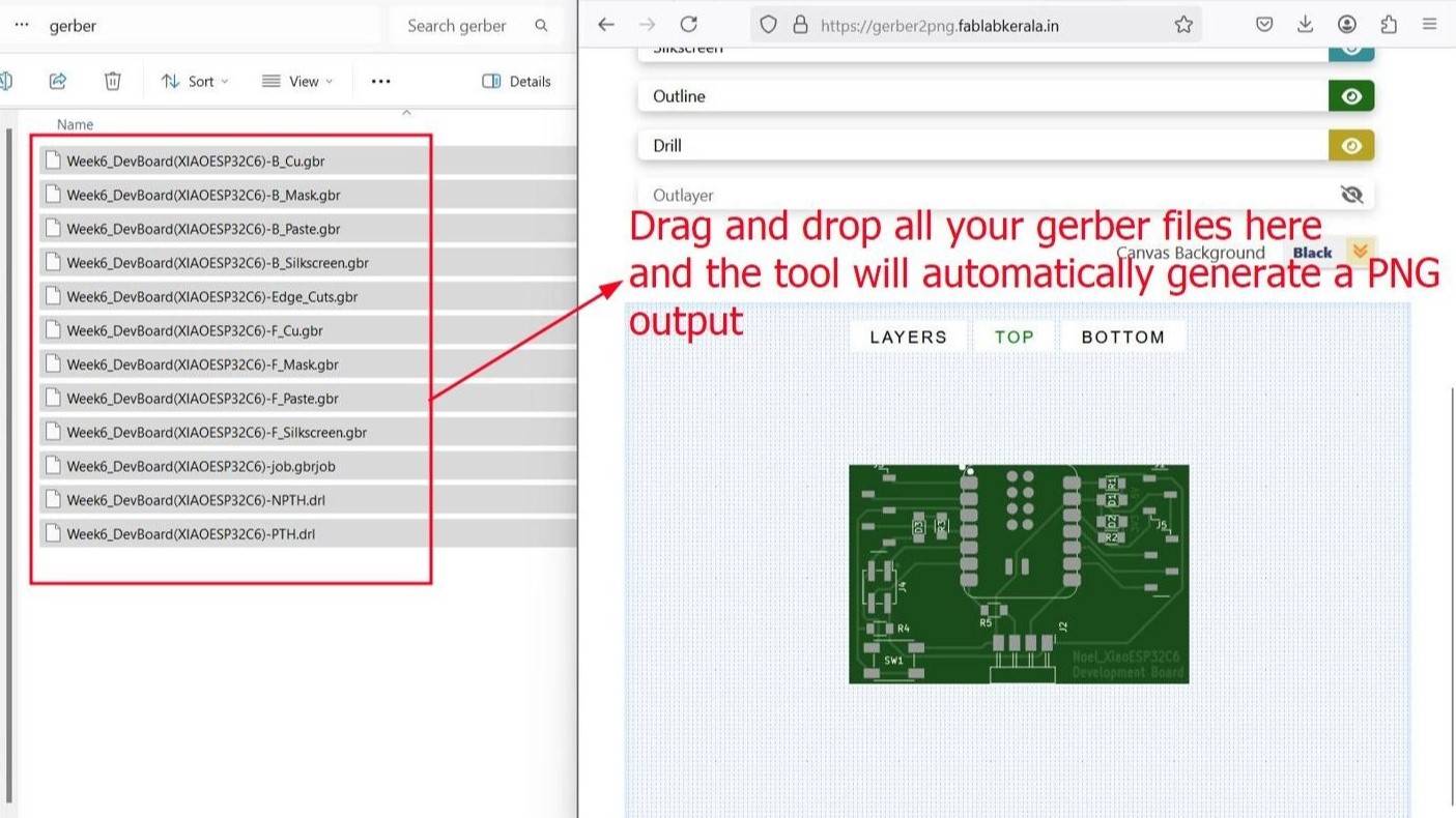
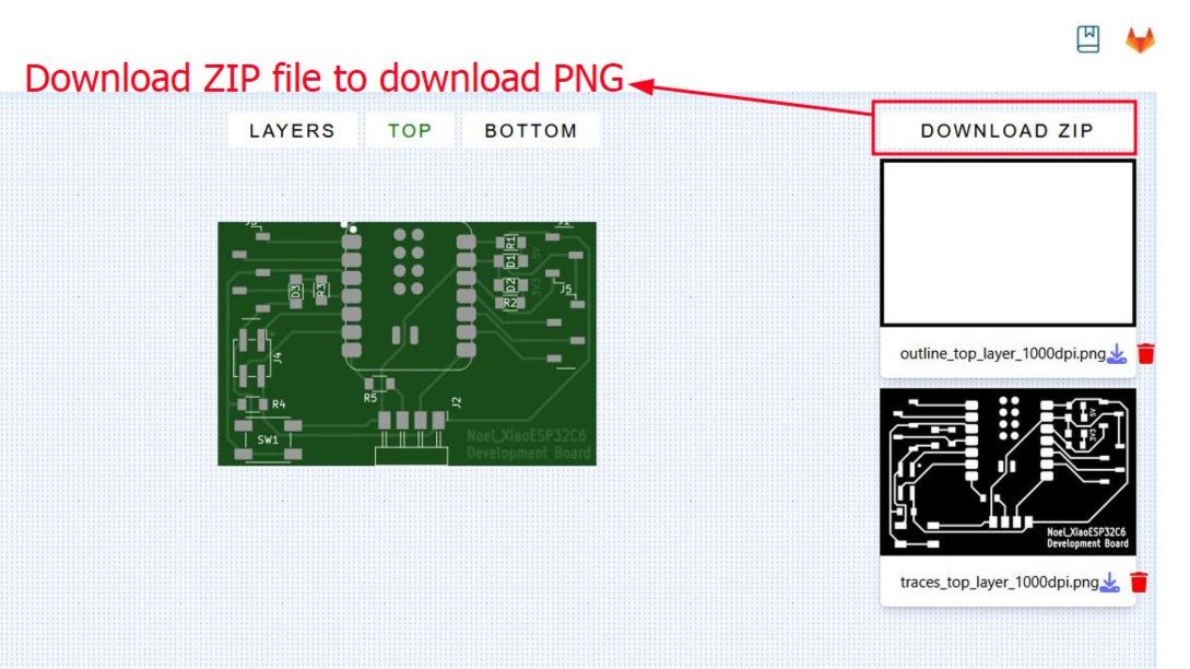
Our lab has made a free to use online Gerber-to-PNG converter tool called Gerber2PNG. I used that convert my Gerber files to PNG files
Preparing the Board
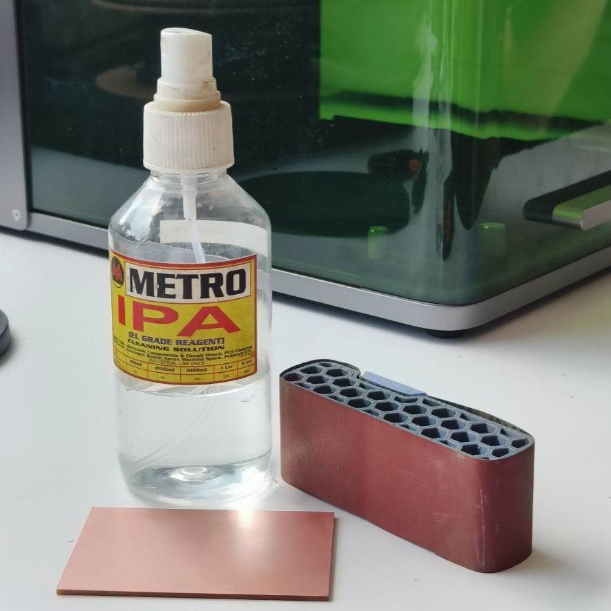
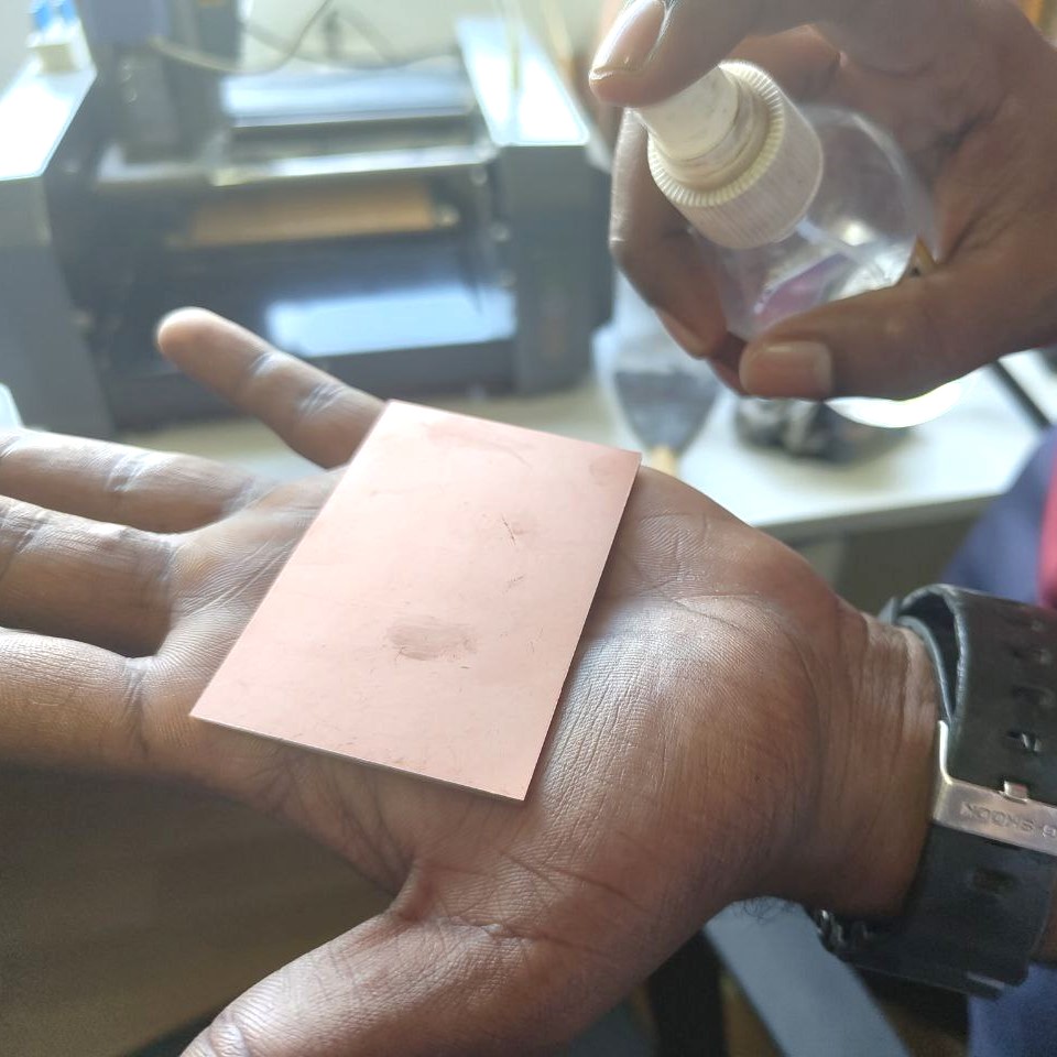
First we remove any smudges using isopropyl alcohol and any preexisting oxidation by sanding
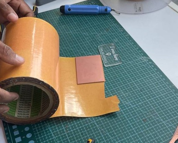
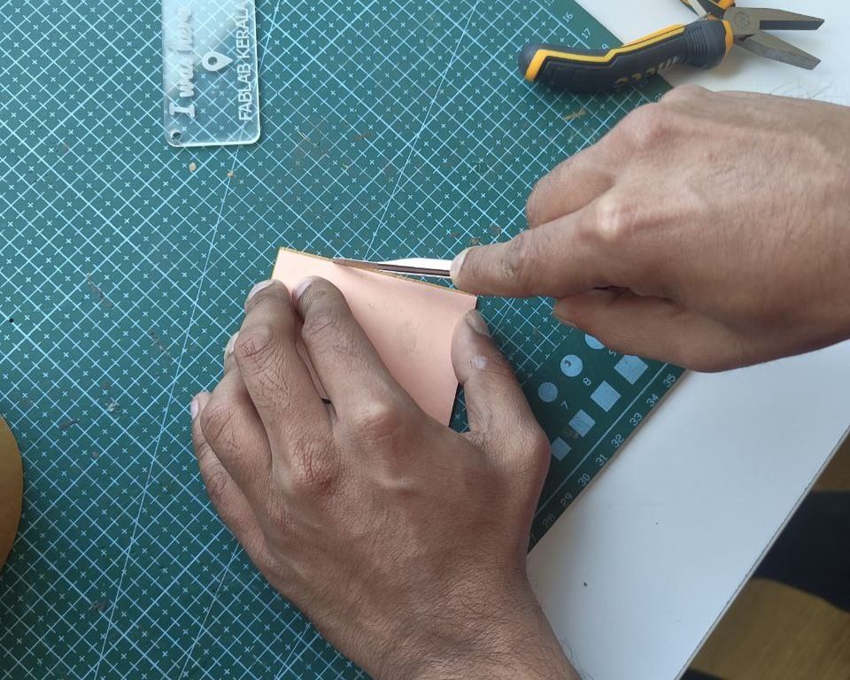
Then we add double sided tape to the back of the PCB and cut it according to the dimensions of the PCB
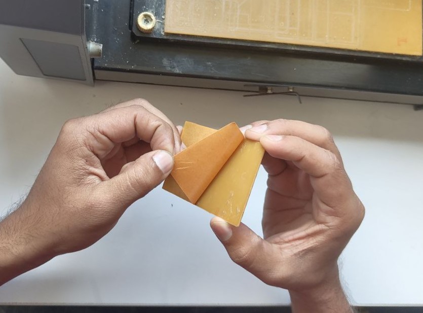
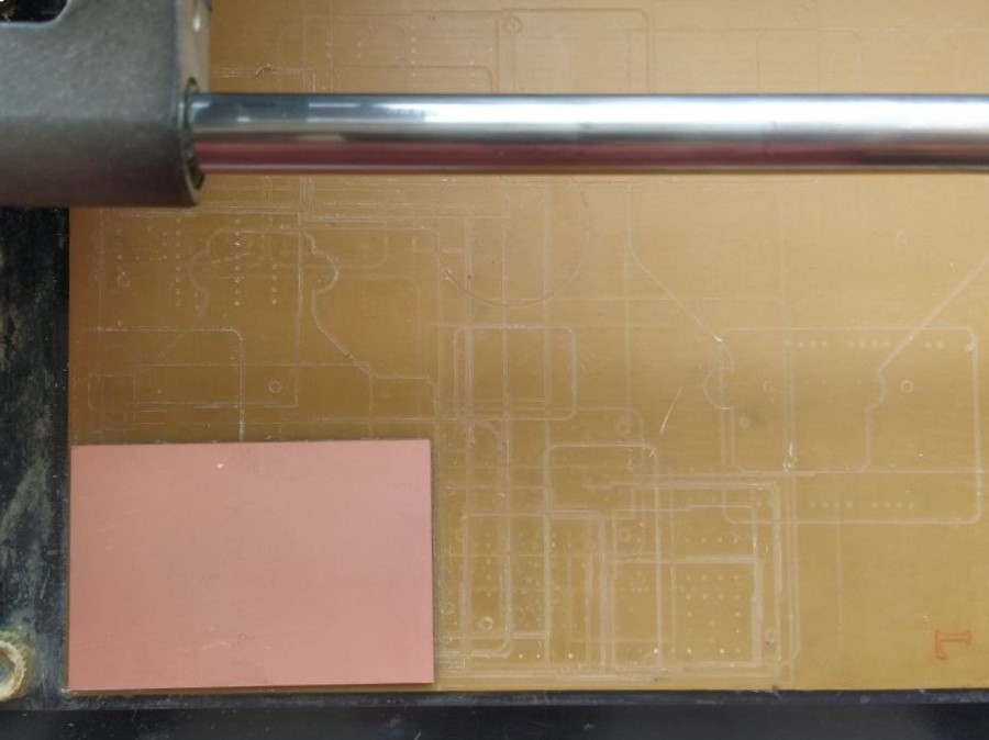
Then we place our board onto the sacrificial layer. The sacrificial layer will be required for cutting to prevent the bit from damaging any other surfaces or getting damaged. The sacrificial layer we use is just some old boards that are not usable.
Using MODS
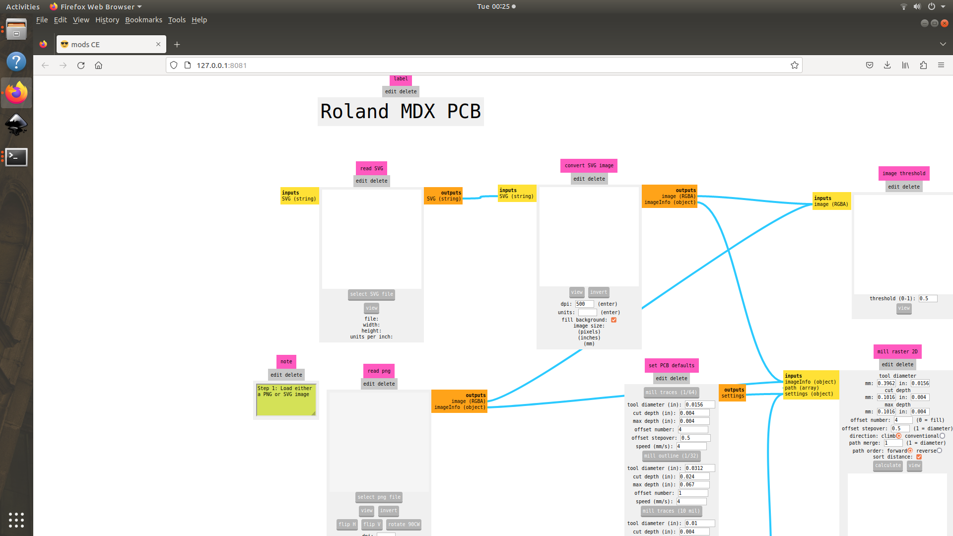
We will be using MODS to mill our PCB. To do that, we first go to the Desktop of the system connected to the milling machine and open the mods_master folder in the terminal and type bash start servers and hit Enter, which lets us get redirected directly to the mods webpage.
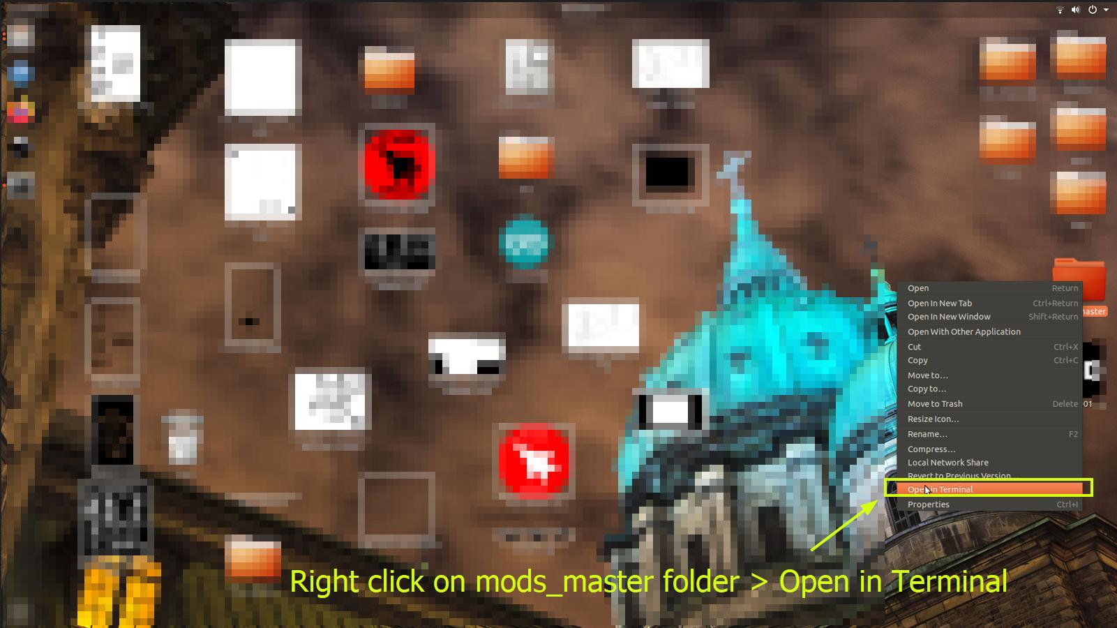
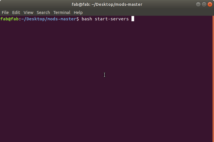
Then we right click anywhere on the page>Program> Open program> PCB under MDX mill
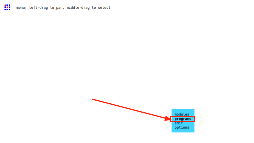
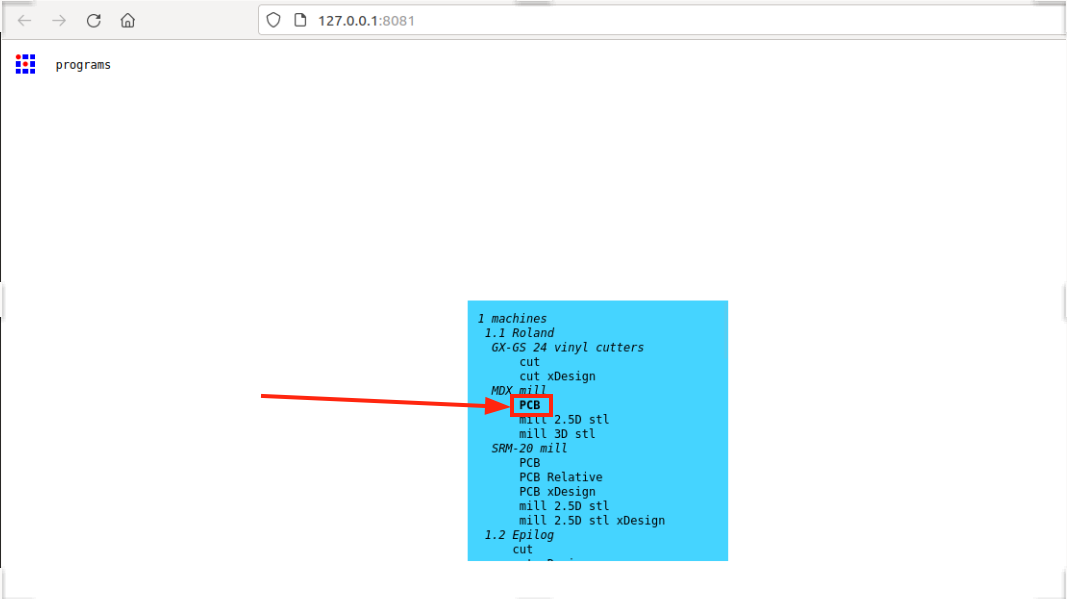
The MODS page has been sucesssfully set up
Milling Traces
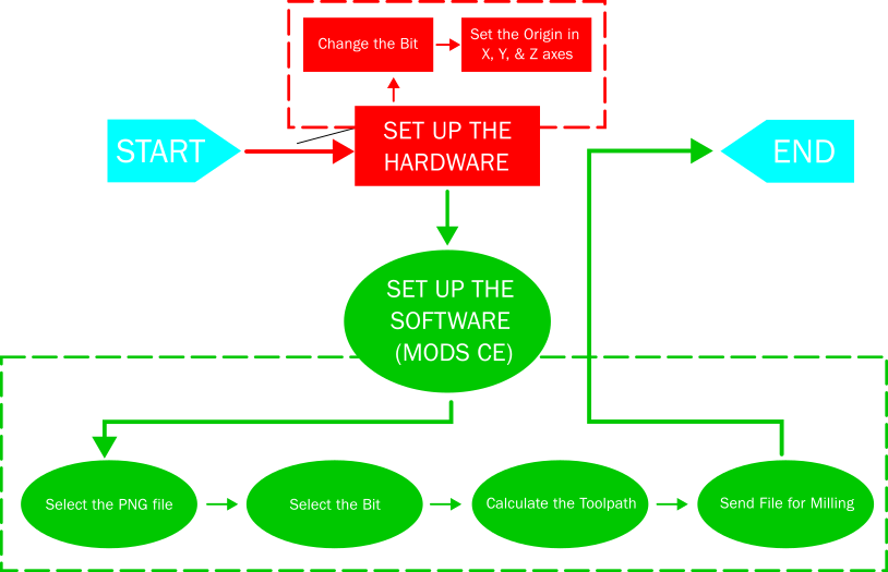
To mill a PCB, I use the following workflow.
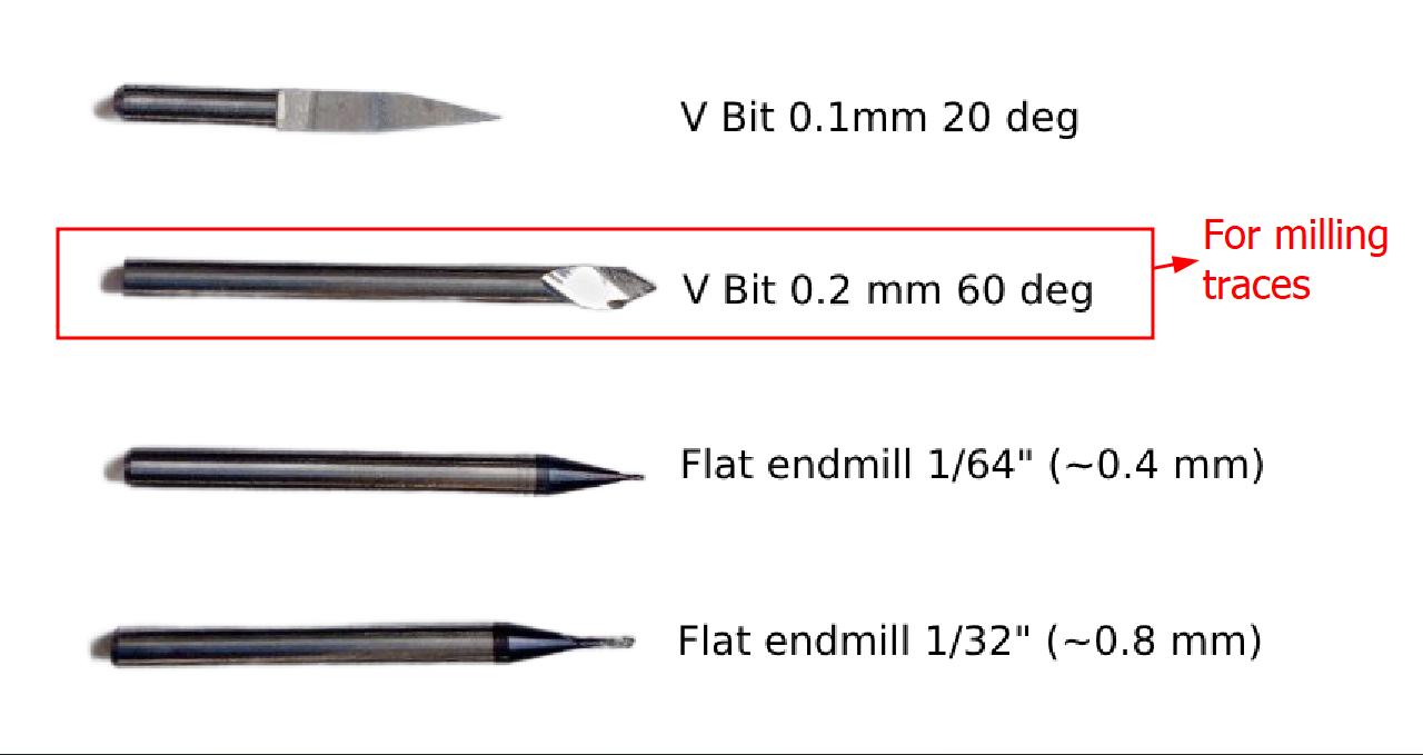
For tracing we prefer using the 0.2 mm V bit becuase it is cheaper than the flat end mills and can make finer cuts as shown in the group assignment.
We press position to replace the bit to 0.2 mm V bit and calibrate out origin position in X and Y axes.
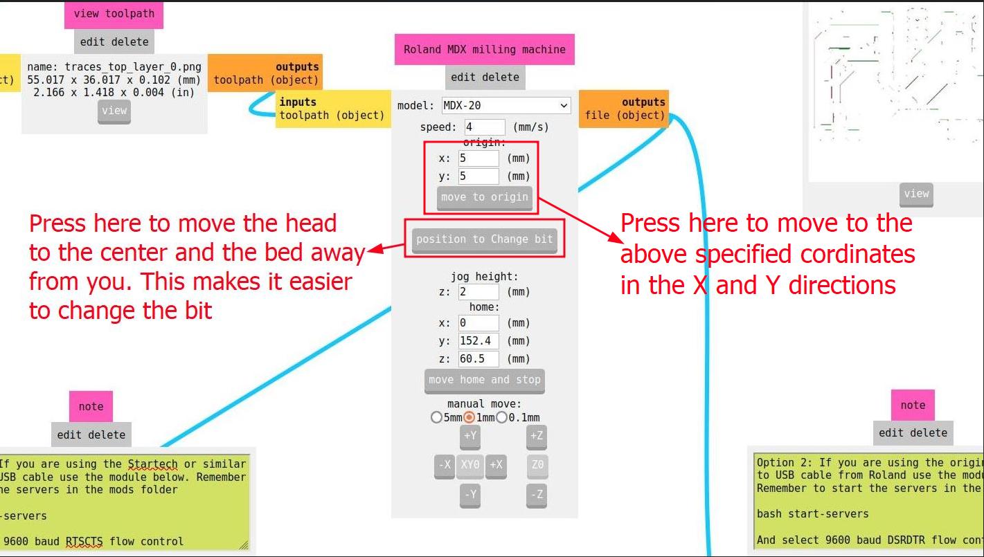
Once the tool reaches the required position, we loosen one of the screws on the spindle using Allen key
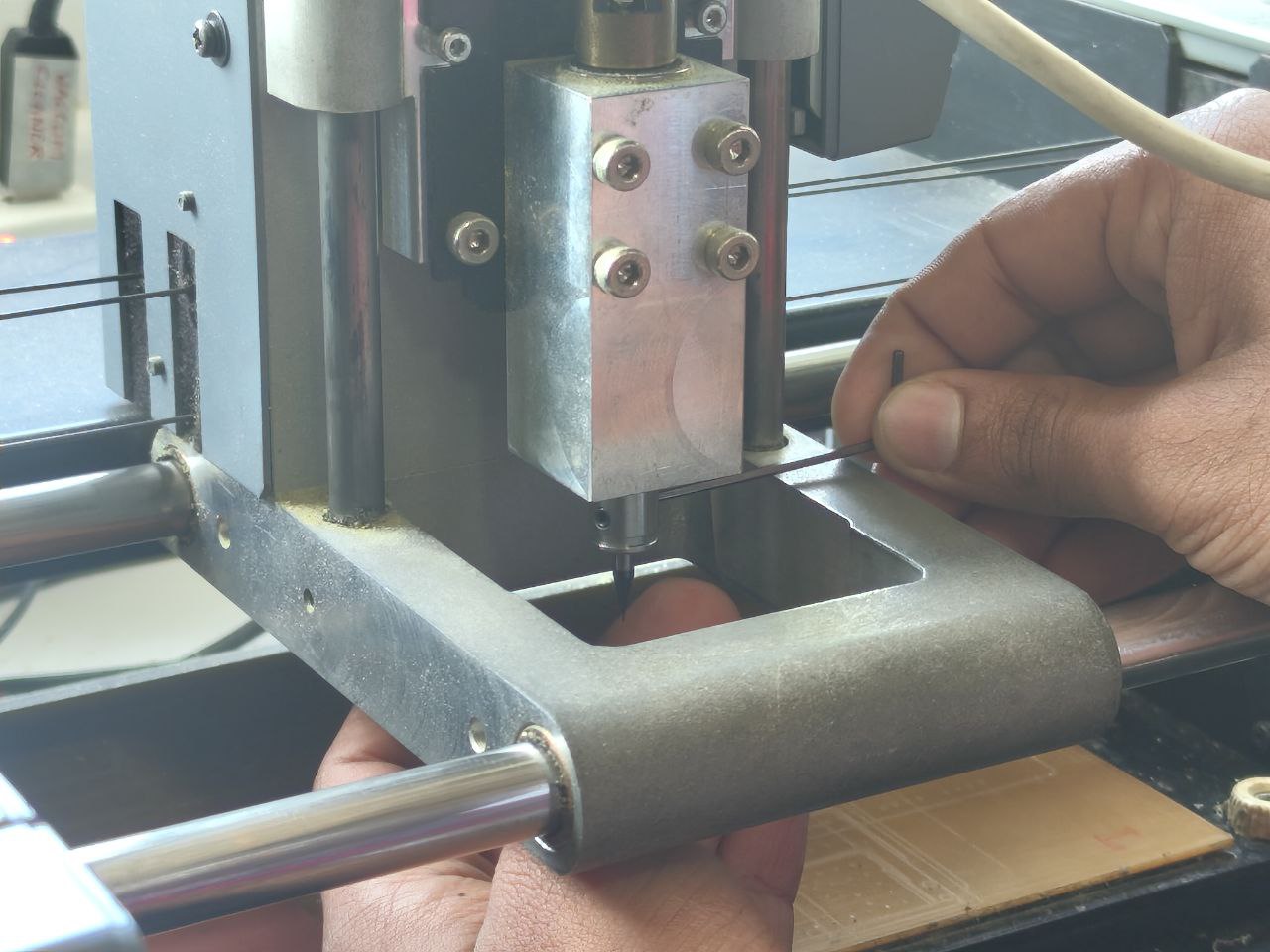
Then we set the Z axis by adding the X-Y coordinates for the origin and pressing 'Move to Origin'. Then we loosen the previously tightened screw using the Allen key while keeping your other hand just below to catch the bit and not let it drop onto the PCB due to its own weight to avoid damage to the tip. Once the bit is lowered slowly and touches the PCB, we tighten both screws on each side of the spindle. We confirm that both screws are tightened before starting the cutting operation to avoid tool breakage due to loose fitting during milling

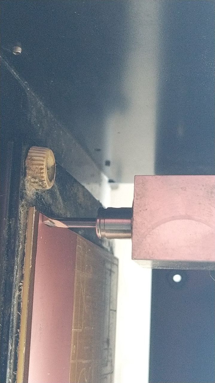
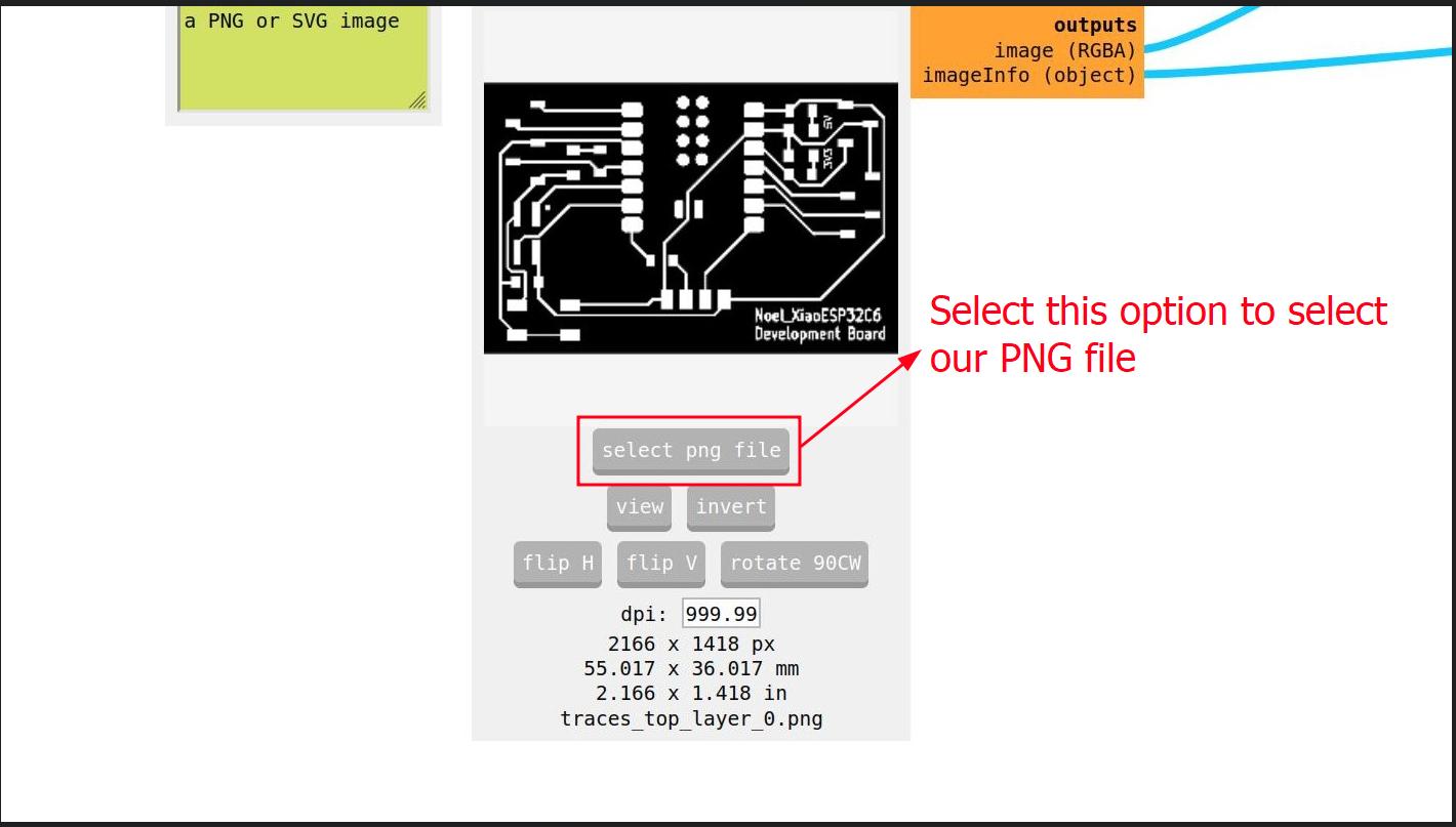
Then we import the PNG file
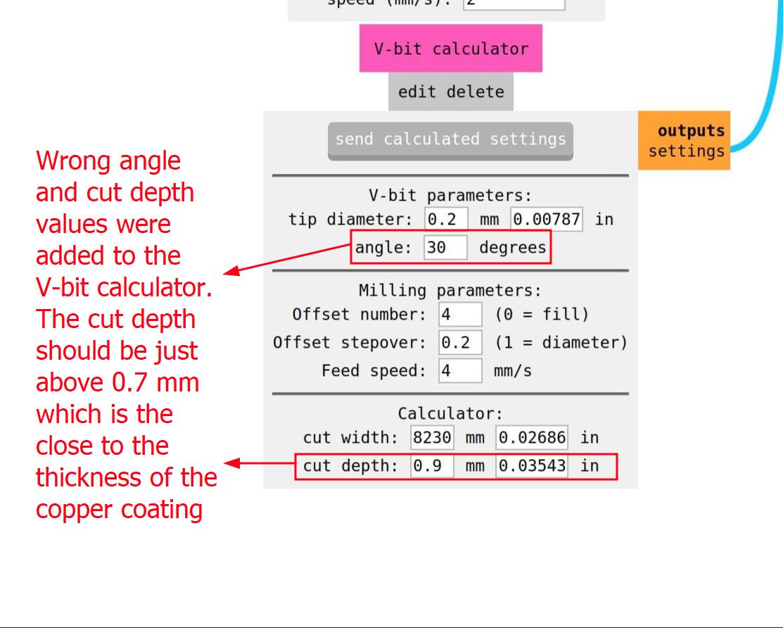
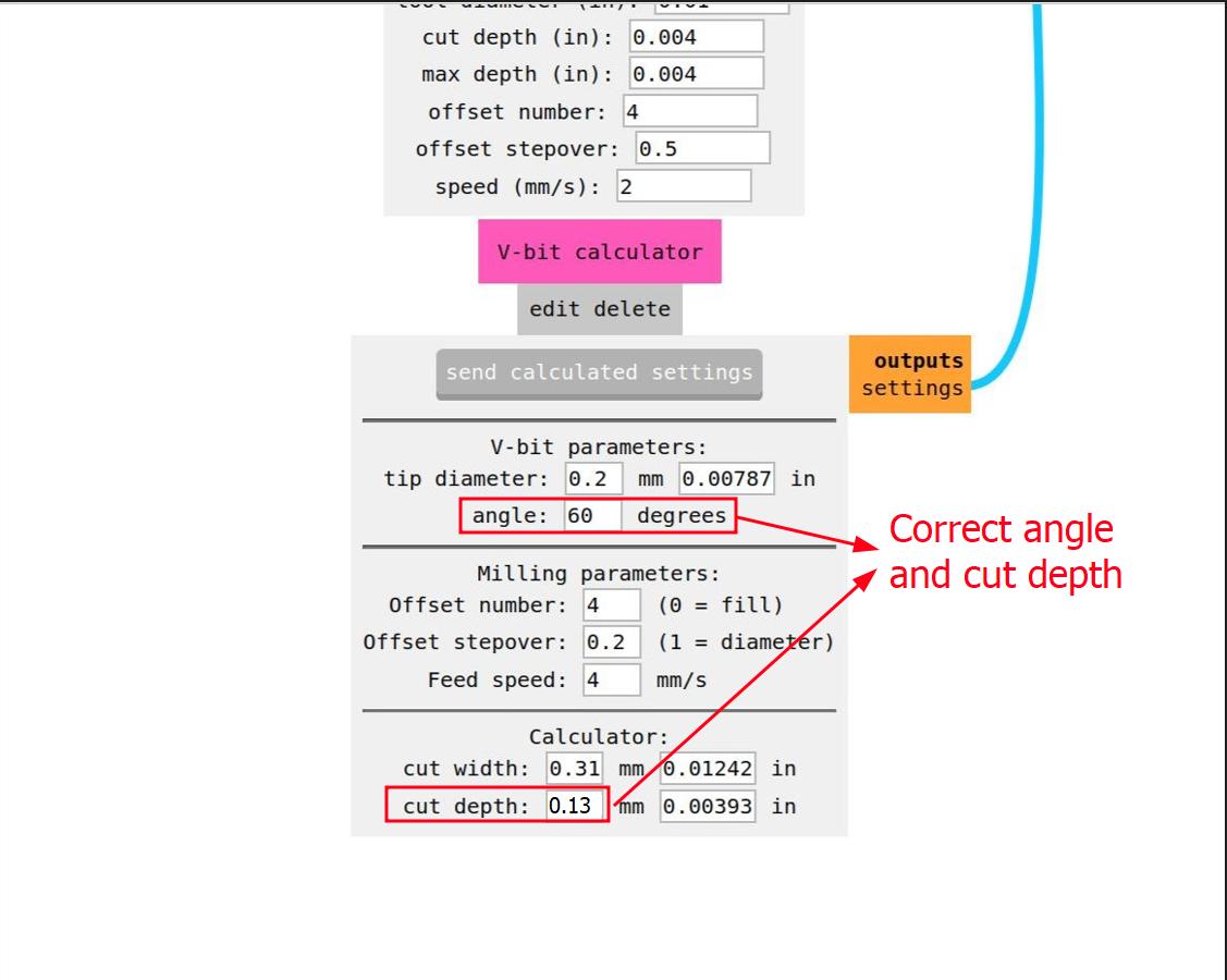
Set the bit presets for the V bit. At first I made an error with the angle of the bit and the cutting depth, which is supposed to be 60 deg and just above 0.07 mm respectively, so the calculated toolpath did not go over many of the features, especially the text. This error was then corrected.
.jpg)
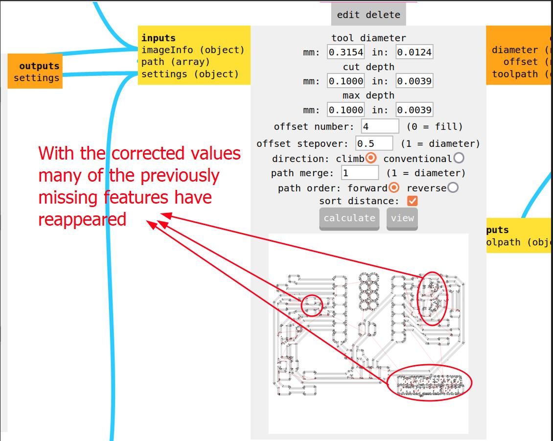
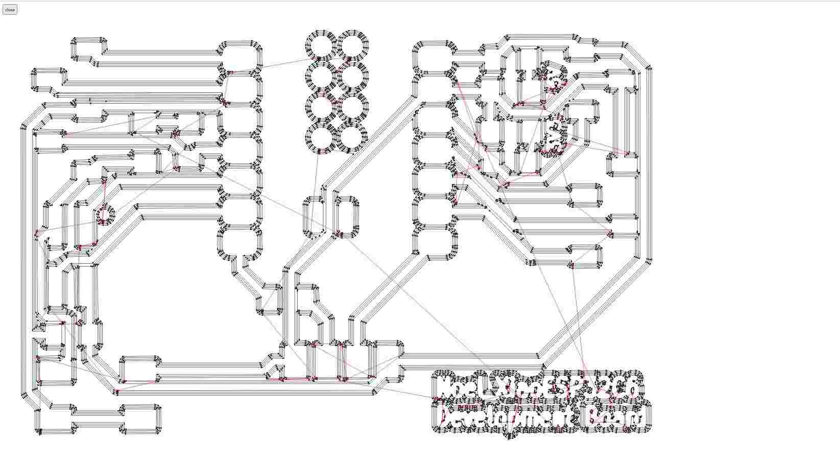
To make sure that the toolpath is correct, I verify it by clicking 'View' in the Toolpath Calculator
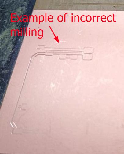
I faced problems with the bit not cutting deep enough to create proper traces, which was fixed by adjusting the 0 of the Z axis and tightening the bit, and also increasing the cut depth to 1.3 mm in the software under V-bit calculator again
Once this issue was fixed the tracing operation worked fine
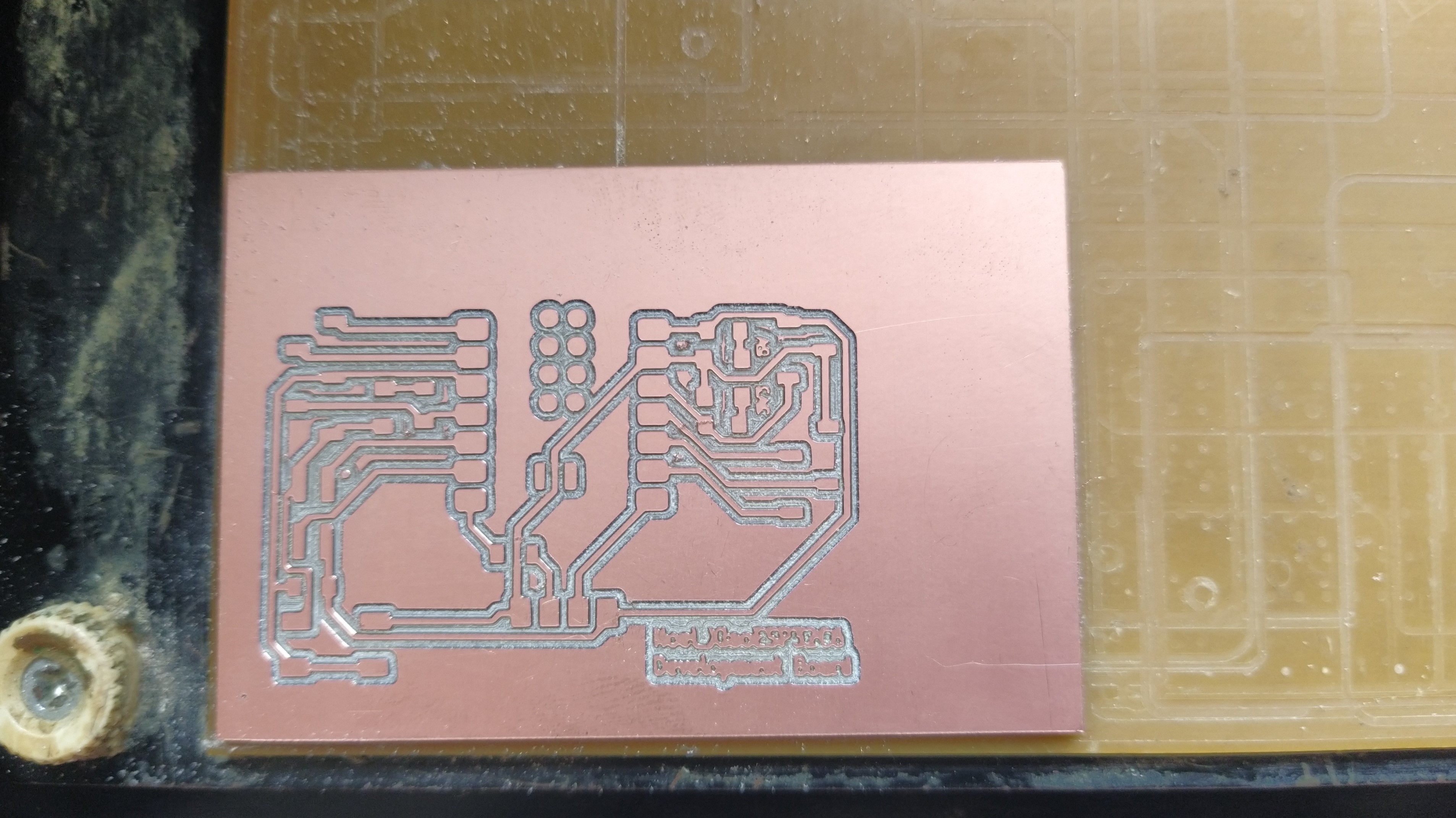
This is how the board looks like after milling traces.
Cutting Board Outline
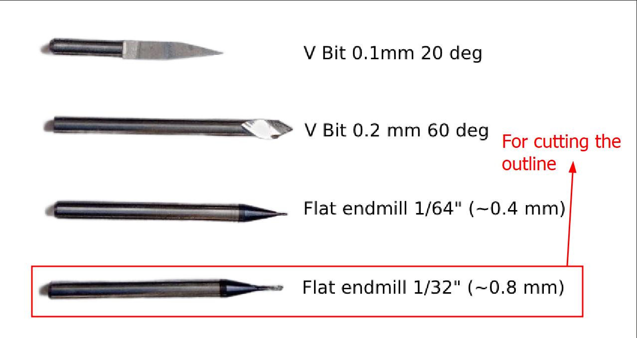
Once the traces were made, its now time to cut the outline of the board. For cutting the board, we will be using the 1/32" (~0.8 mm) flat end mill.
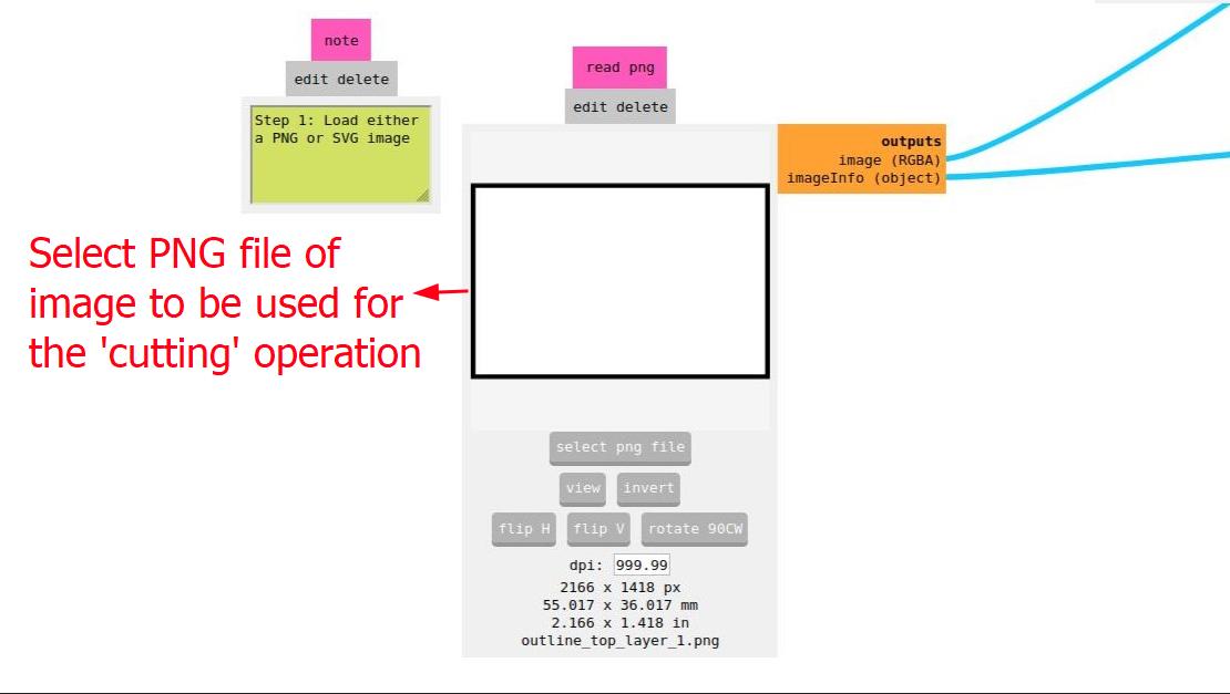
We repeat the same process as before with some minor changes. First we import a different PNG file containing just info on the outline.
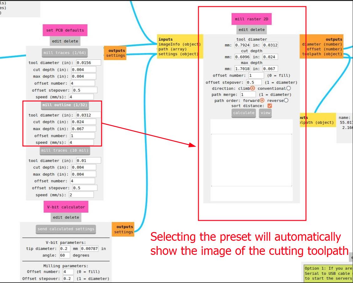
Then we choose the preset for 1/32" (~0.8 mm) bit, before sending the data to calculated in our toolpath viewer
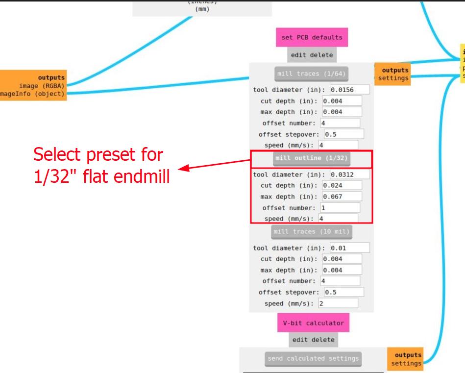
Then we confirm the offset and the stepover cut depth and width. Once confirmed, we send the file to be cut as before
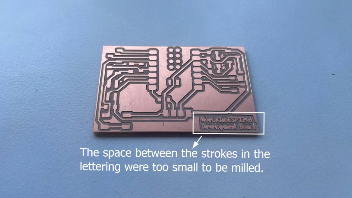
Once done milling, use the vaccum cleaner to clean the surface. Then use the scraper to remove the board and any remaining portion. Then I removed the sticky backing from both pieces and the sacrificial layer. To clean the PCB I use isopropyl alcohol again to. This is how my board looks like after milling. As you can see the width between strokes was too small to be milled.
In case you need to pause at any point in the process, Click 'View' button on the machine. This is a toggle button. When the light above View button is ON, it means that the milling machine has been paused. To continue, you simply have to click View once more, and the lights turns OFF, indicating the machine is now running.
If you make an error during the milling operation and need to restart, you do the following:
Click View to pause the machine and inspect to see if you need to restart the milling operation from scratch. If yes, then click 'Disconnect from socket' in MODS software, click both Up and Down buttons on the machine at the same time to clear all the data. The lights will flash to indicate that the data is being removed. Once the blinking stops, the process has been completed. Then you press 'View', followed by 'Connect to the socket in the MODS page. You can now restart the process.
Bill of Materials (BOM)
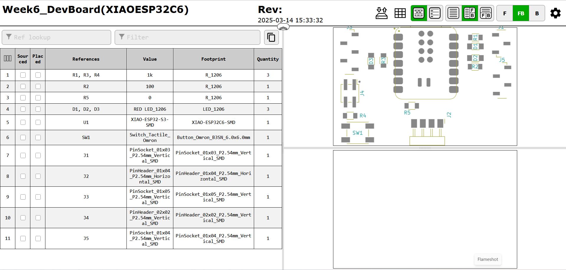
I added an interactive BOM plugin in KiCAD to help automatically generate a BOM of my PCB design.
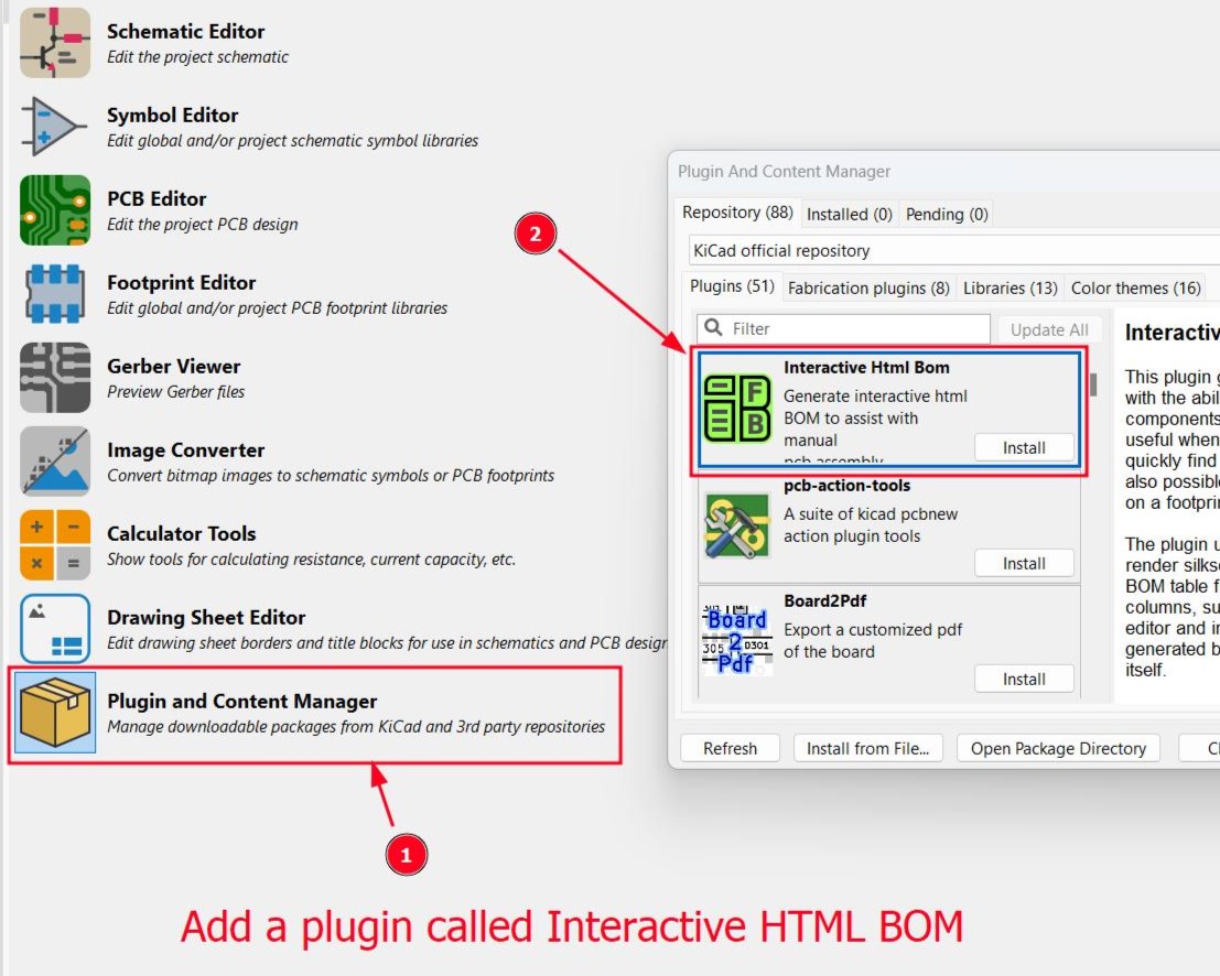
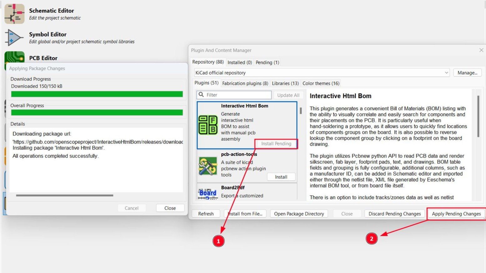
Then go to PCB Editor > Interactive BOM > Generate PCB. Your BOM will be automatically generated as an HTML page that can be saved and shared with others
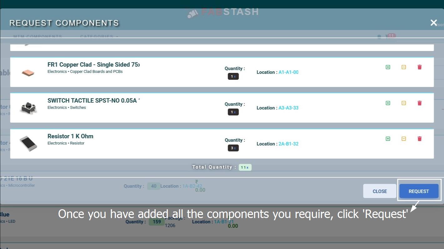
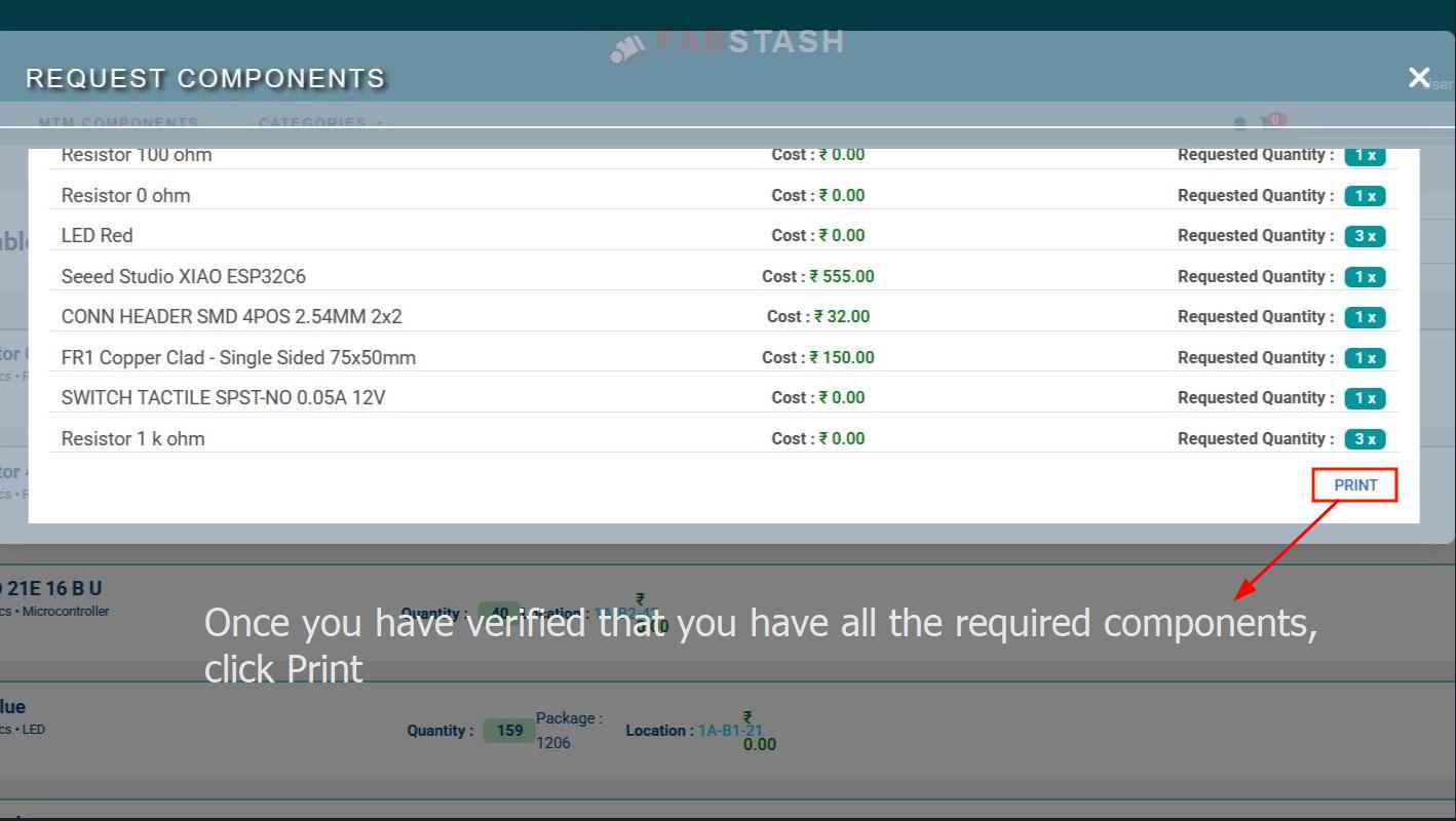
Then we go to Fab Stash, our inventory page at Fab Lab Kochi. I requested all the components I need and printed it out on an A4 sheet. Since the site is still under active development, I faced problems while printing using Mozilla Firefox and Google Chrome, but it worked fine on Microsoft Edge
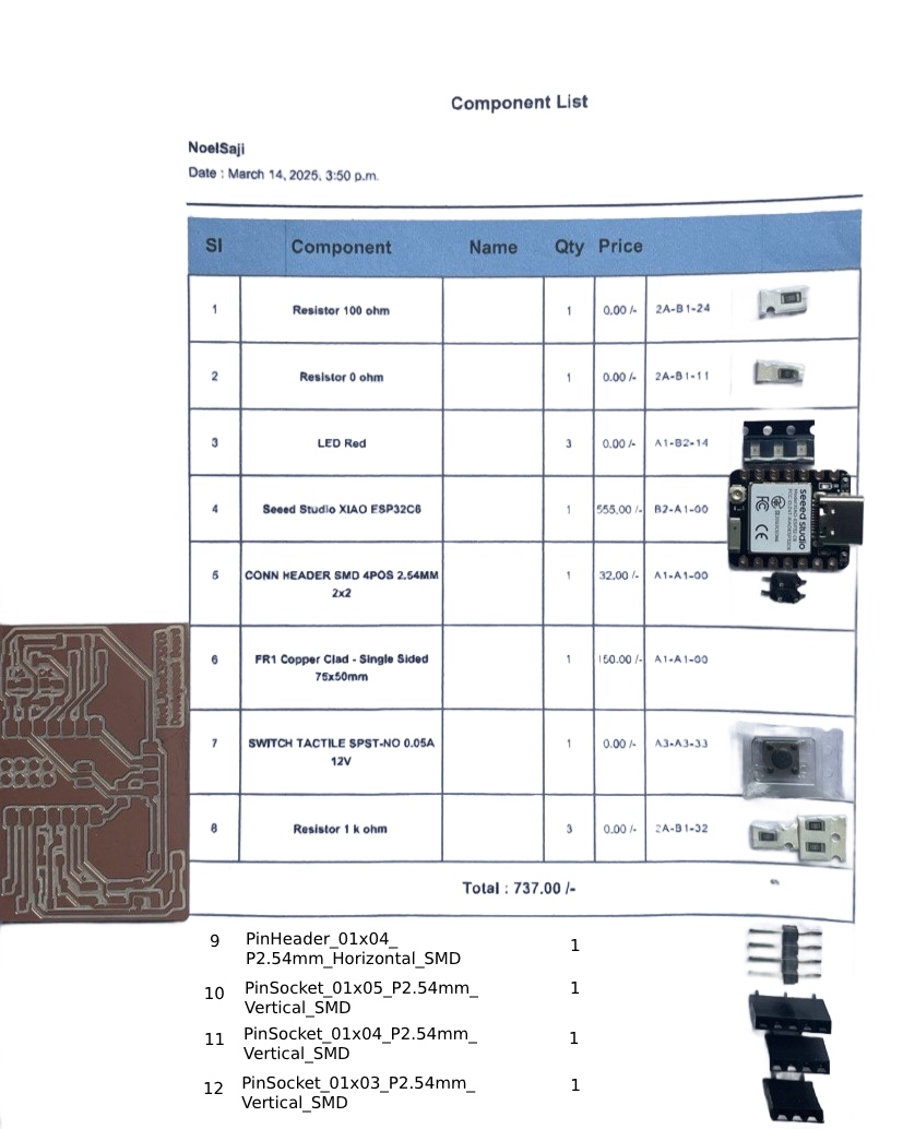
Once my BOM sheet is printed, I add sticky tape to one column, take items from the inventory and stick them on the sticky tape.
Soldering
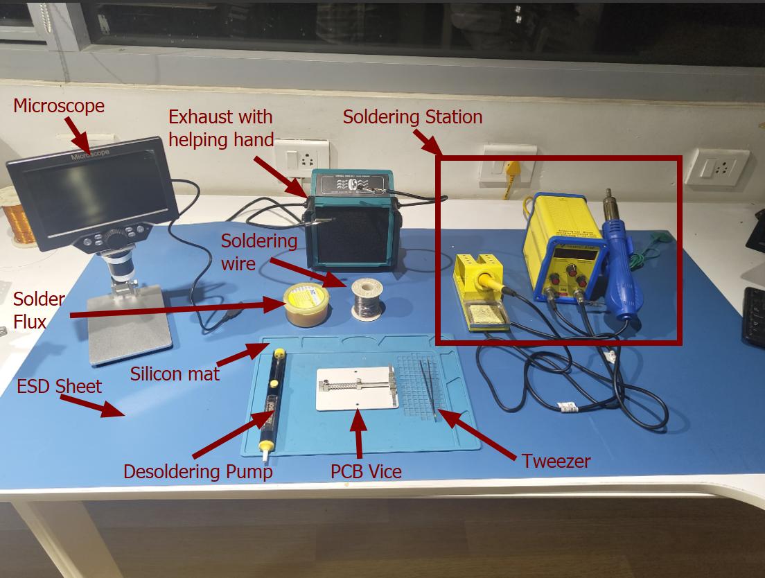
It is important to use a mask while soldering since the fumes are posionous. Also we 'tin' the end of the iron every time before we start using it to help with making proper connections.
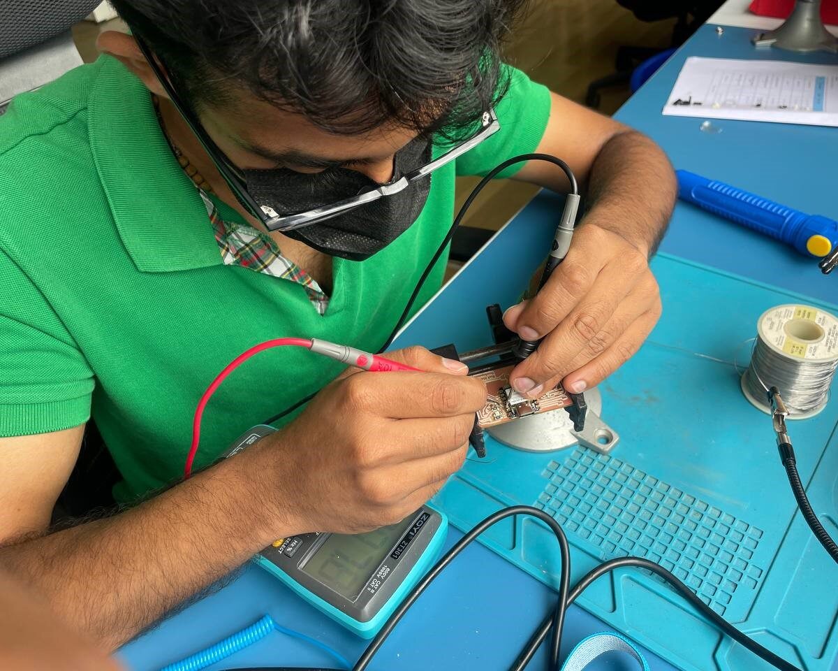
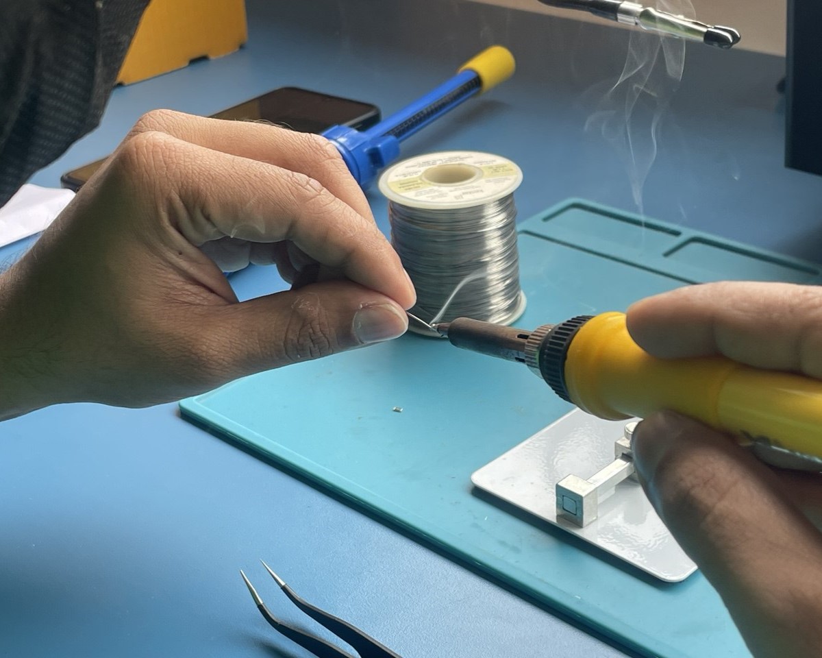
There is an order we follow while soldering components to ensure easy assembly. First we start with the smallest components like the resistors & diodes. Then we go for flat components over tall compennts because of is easier to solder them later, for example the Xiao Board itself. Then at the last we solder the connectors because theye are the tallest.
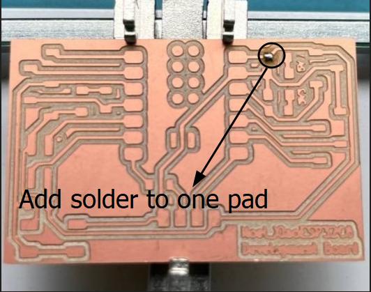
First we have to add solder to one of the pads, then add the resistor, then heat using iron to form connection.
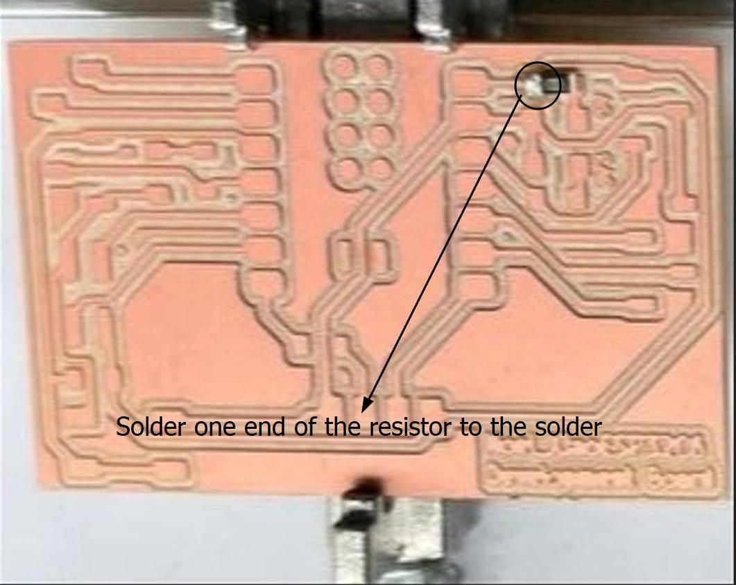
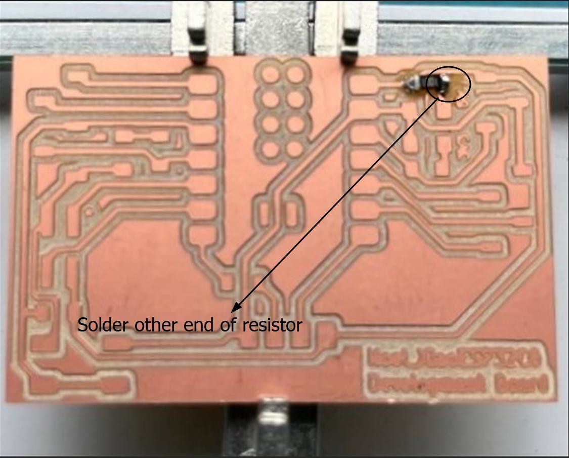
Tips to follow while soldering
- Leave space for each pad to be exposed for good soldering
- Hold the tweezers carefully, don't drop them to avoid damaging the tips.
- Hold the tweesers in the left and the iron in the right in your right hander, keep rotating PCB to be oriented
- Holder solder in left and iron in right, keep rotating PCB to be oriented
- Start with the smallest components and work your way larger
- After adding solder to one pad, place the resistor next to bead and push instead of placing on top. Once on top pad, heat the top of the resistor
- I used the pinmapping to confirm the PWR and GND connections using the Pinmapping diagram
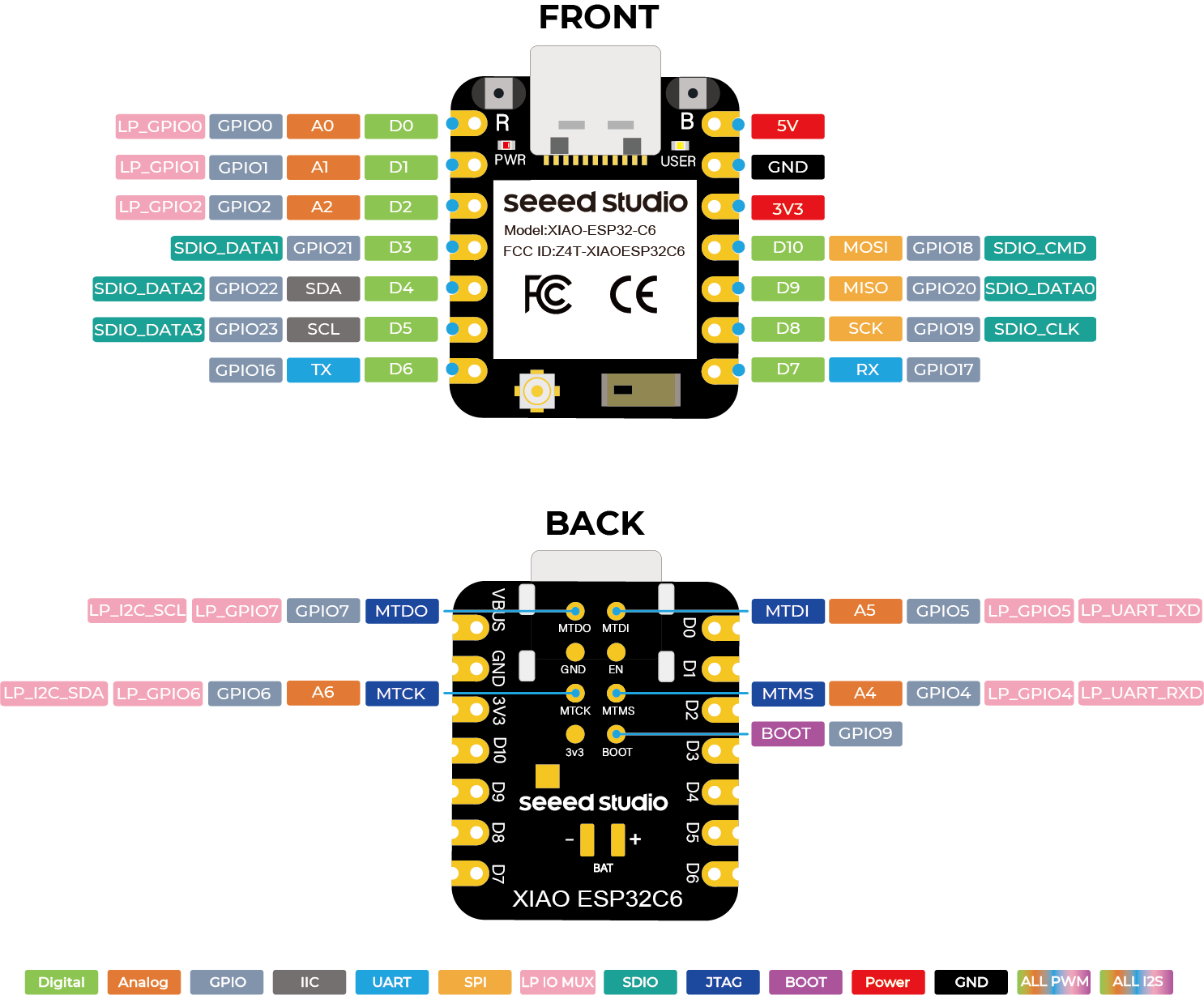
Difficulties I faced while soldering
- Soldering diodes was harder because their terminal connections that I can touch with the iron were smaller
- Make sure to verify the placement of each component before and after soldering the first pad. Made a mistake with diode and resistor placement, have to desolder later before all connectors have been placed
- Tweezers pressing too hard causing components tl fly off
- For switch connect one corner, then opp corner, then rest 2 panels
- Have to adjust vice to allow proper placement of XIAO
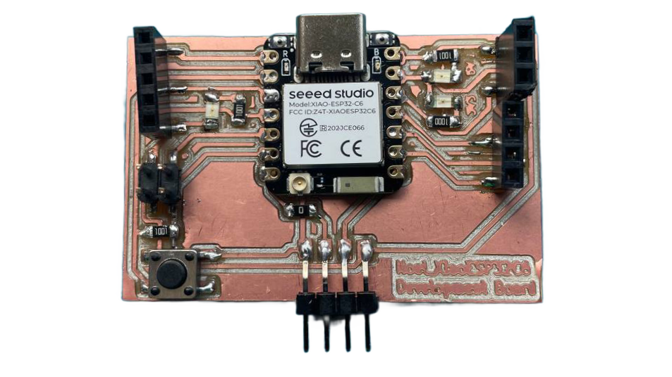
Now I just have to repeat the same process for the rest of the components. This is how my PCB looks like once done
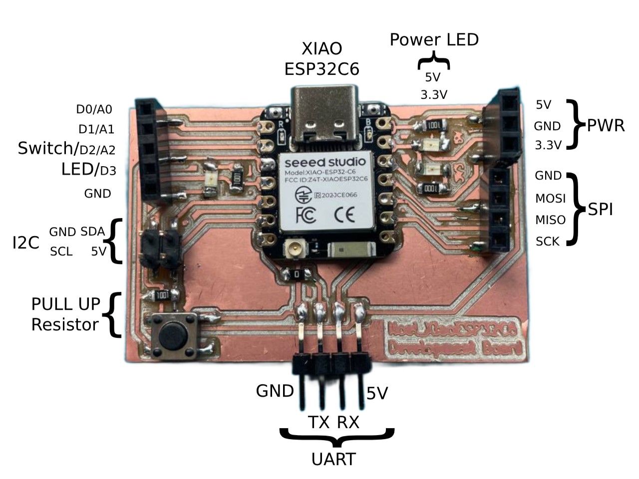
Verification
First we confirm the quality of our connections using a microscope.
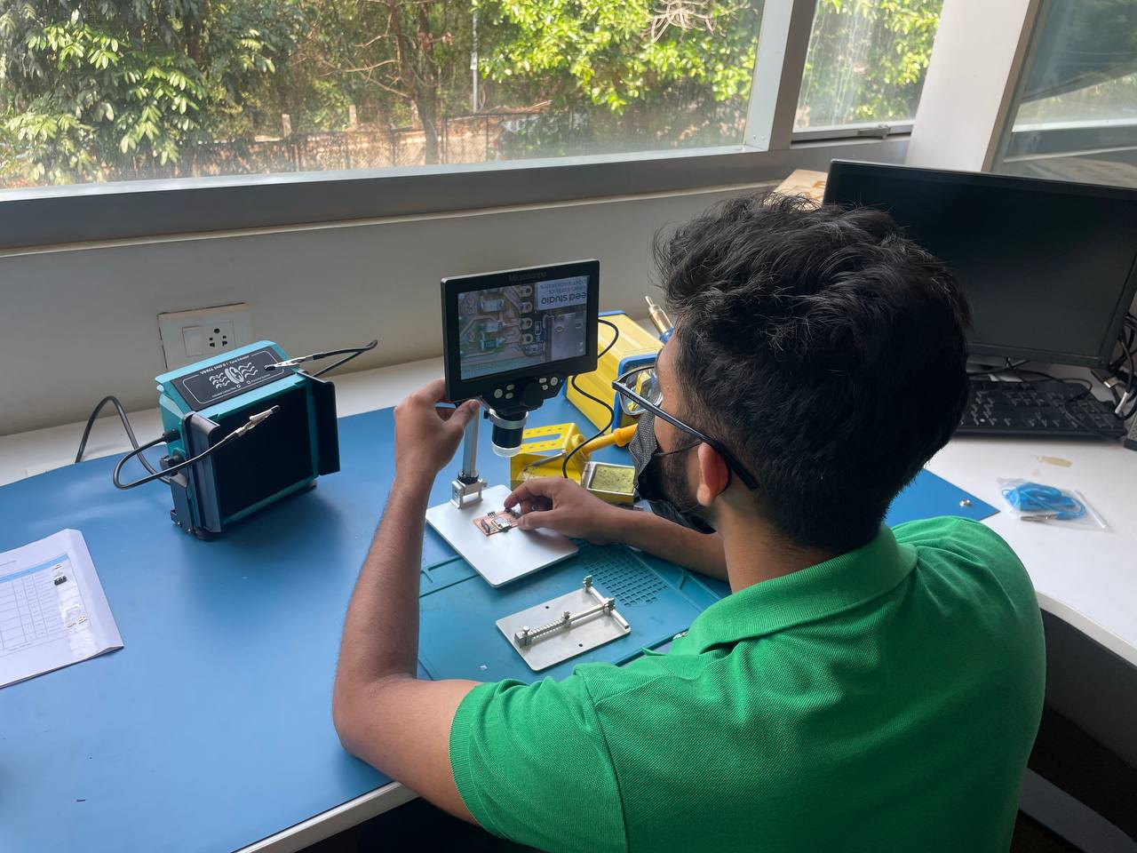
So these are the following errors I saw in my board
.jpg)
.jpg)
.jpg)
.jpg)
Programming
Once all the connections have been checked and and errors in soldering have been corrected, it is now time to test if we can program the board using the Arduino C++ LED Blink program. I followed this article by Xiao Seeed Studio to program the board on Arduino IDE. To know more read my documentation in Week 4: Embedded Programming
Program 1: Xiao On-board LED Blink
First tested onboard LED on Xiao using Example Blink program
Program 2: Develeopment On-board LED Blink
Now to test LED I have put on my dev board. Using schematic and pinmapping diag- LED is connected to pin 4 (also called GPIO21, or D3)
Here is my code working on my self-designed PCB development board
    #define LED D3

    void setup() {

    pinMode(LED, OUTPUT);
    }

    void loop() {
    digitalWrite(LED, HIGH);  // turn the LED on (HIGH is the voltage level)
    delay(1000);                      // wait for a second
    digitalWrite(LED, LOW);   // turn the LED off by making the voltage LOW
    delay(1000);                      // wait for a second
    }
Program 3: Controlling an LED using a Switch
    #define LED D3
    #define Switch D2
    int Sval;

    void setup() {
    pinMode(Switch, INPUT);
    pinMode(LED, OUTPUT);
    Serial.begin(9600);
    }

    void loop() {
    Sval=digitalRead(Switch);

    if (Sval==1){
        digitalWrite(LED, HIGH);
    }

    else if (Sval==0){
        digitalWrite(LED, LOW);
    }

    Serial.println(Sval);
    }
Program 4: Controlling an LED via Serial Monitor
I used the board I made to control an LED via Serial Monitor. Serial Monitor is a software application usually found in Integrated Development Environemnts to read and write data with microcontrollers using a serial connection.
                            #define LED D3
                            char user;

                            void setup() {
                            pinMode(LED,OUTPUT);
                            Serial.begin(9600);
                            }

                            void loop() {
                            user = Serial.read();

                            if (user == '1') {
                                digitalWrite(LED, HIGH);
                                Serial.println("ON");
                            }

                            else if (user == '0') {
                                digitalWrite(LED, LOW);
                                Serial.println("OFF");
                            }
                            }
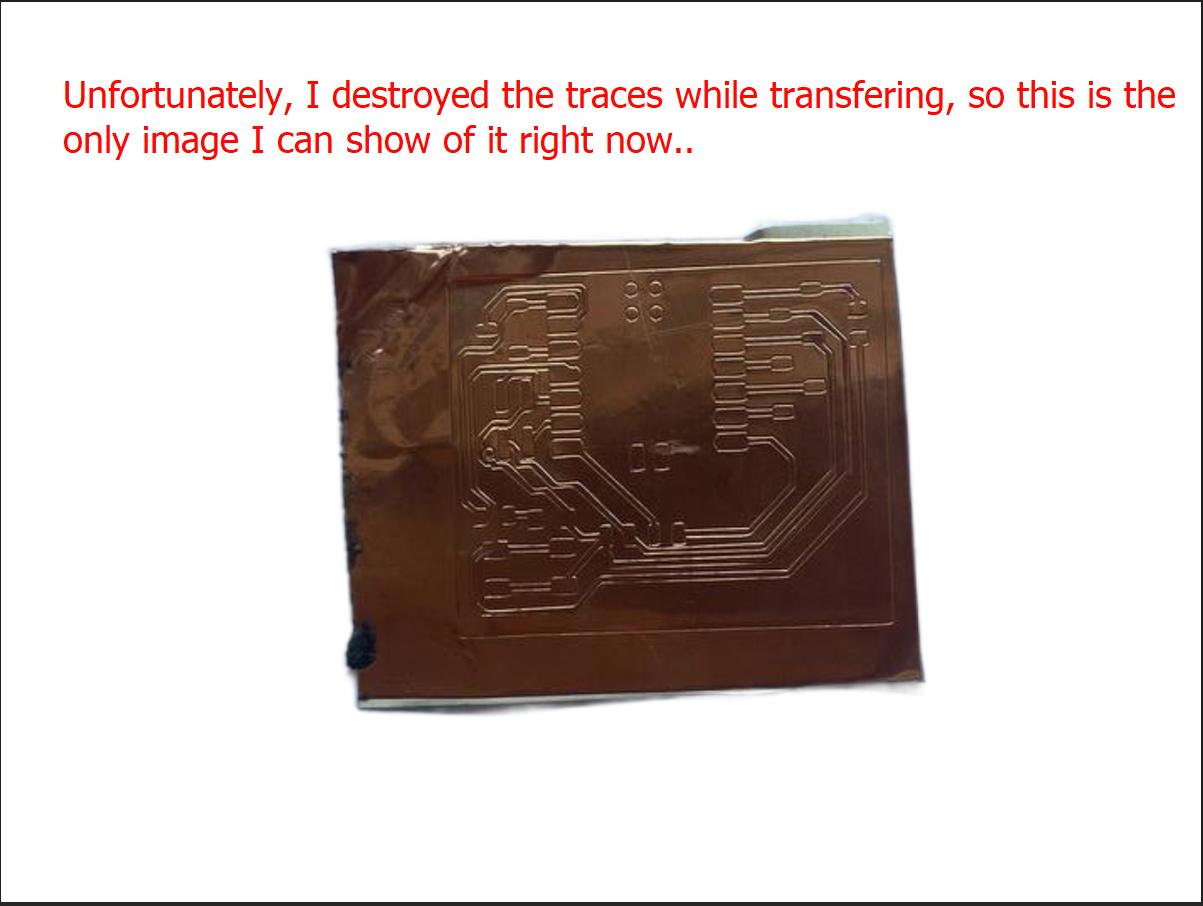
Make the custom development board using another process.
Make a flexible circuit using vinyl cutter
Conclusion
This week we learned the following:
- To characterise the design parameters of different machines for the purpose of making PCBs.
- To order PCBs from PCB houses
- To fabricate our own circuits as PCBs; including milling, soldering, and testing
Mistakes and Solutions
- Errors with V-bit calculator: the angle of the bit and the cutting depth, which is supposed to be 60 deg and just above 0.07 mm respectively, so the calculated toolpath did not go over many of the features, especially the text. This error was then corrected.
- Errors with Z position of milling bit: I faced problems with the bit not cutting deep enough to create proper traces, which was fixed by adjusting the 0 of the Z axis and tightening the bit, and also increasing the cut depth to 1.3 mm in the software under V-bit calculator again
- Using FabStash in Edge: Since the site is still under active development, I faced problems while printing using Mozilla Firefox and Google Chrome, but it worked fine on Microsoft Edge
- Soldering SMD resistors: After adding solder to one pad, place the resistor next to bead and 'push' instead of placing it on top. Once on top pad, heat the top of the resistor
- Checking connections: Made a mistake with diode and resistor placement, have to desolder later before all connectors have been placed. Make sure to verify the placement of each component before and after soldering the first pad.
- Leaving gaps between the component terminal and pads: Leave space for each pad to be exposed for good soldering
- Follow an order while soldering components: First we start with the smallest components like the resistors & diodes. Then we go for flat components over tall components because of is easier to solder them later, for example the Xiao Board itself. Then at the last we solder the connectors because they're are the tallest, hence they will cause the most issue in soldering components if they were placed before
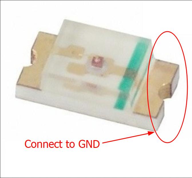
- LED polarity: Connected LEDs in the reverse bias position, the green line indicates GND
