6. Electronics Design
Objectives
This week's assignment tasks are listed below:
- group assignment:
- use the test equipment in your lab to observe the operation of a microcontroller circuit board
- individual assignment:
- use an EDA tool to design a development board that uses parts from the inventory to interact and communicate with an embedded microcontroller
- extra credit: try another design workflow
- extra credit: simulate your design
- extra credit: design a case around your design
Group Assignment
For our group assignment we used the following test equipment in our lab to observe the operation of a microcontroller circuit board
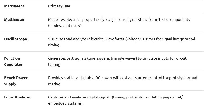
Here is the link for the group project
Training
28-02-2025: Our instructors organised a class with Midhun Joseph (FA 2024) to learn how to use KiCAD by designing a demo PCB.
KiCAD Project Creation
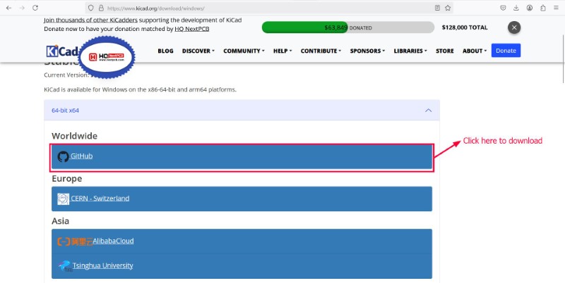
First we must define what an EDA tool is. According to this article, the full form of EDA is Electronic Design Automation. An EDA tool (lik KiCAD) is any tool that is used to create CAD models of electronics system like PCBs. First I downloaded KiCAD Version 9. To download click here.
First we were taught to add symbols and footprints for PCB components in case it is not available natively in KiCAD. For this, we used a site called Snap Magic EDA.

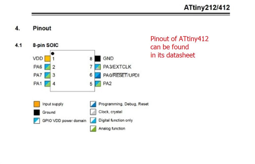
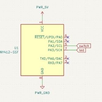
Since the symbol for Attiny1614 is not available, we made our own using the help of the datasheet in SnapEDA.
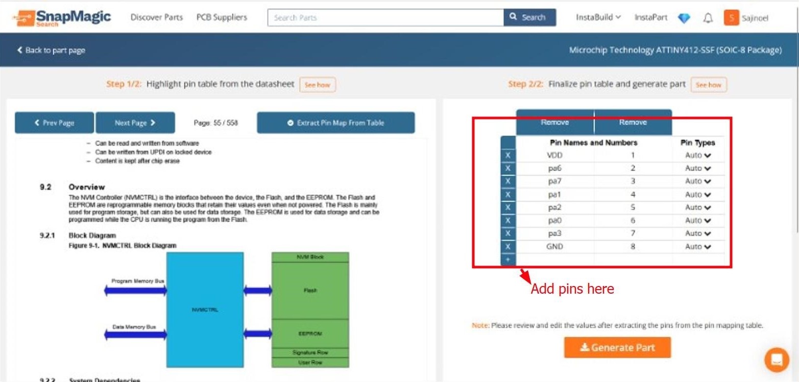
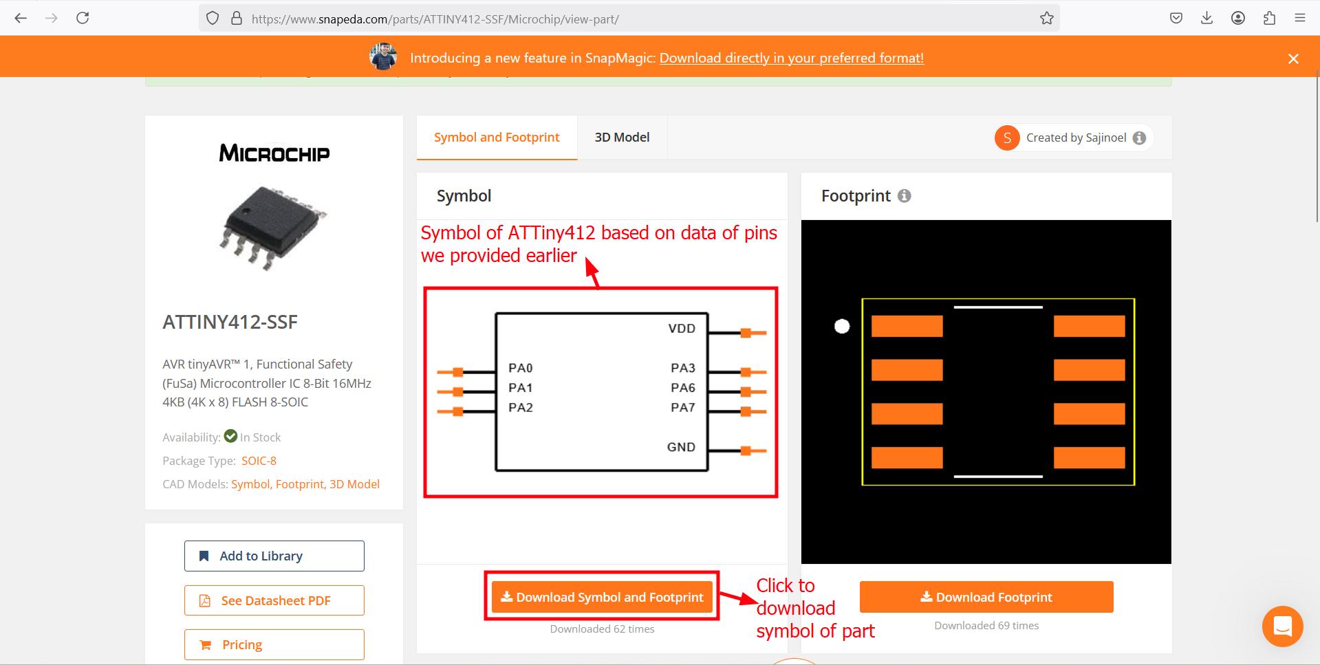
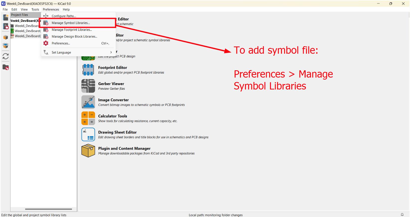
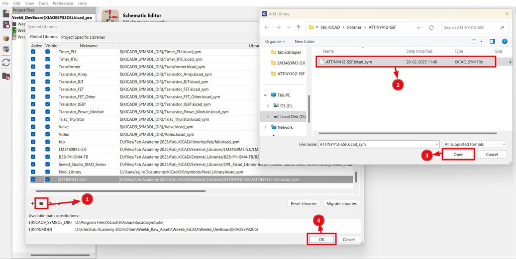
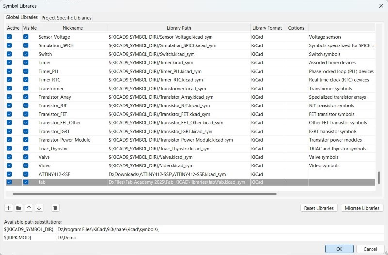
You can only add symbols and footprints after you extract the folder. To add the symbol file, we go to Preferences > Manage Symbol Libraries > Select 'Folder' icon (Add existing library to table) > Select the 'ATTINY412-SSF' Folder > Select the corresponding .kicad_sym file. > Select 'Ok'
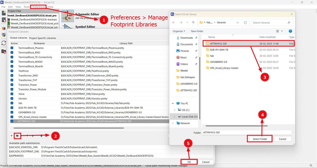
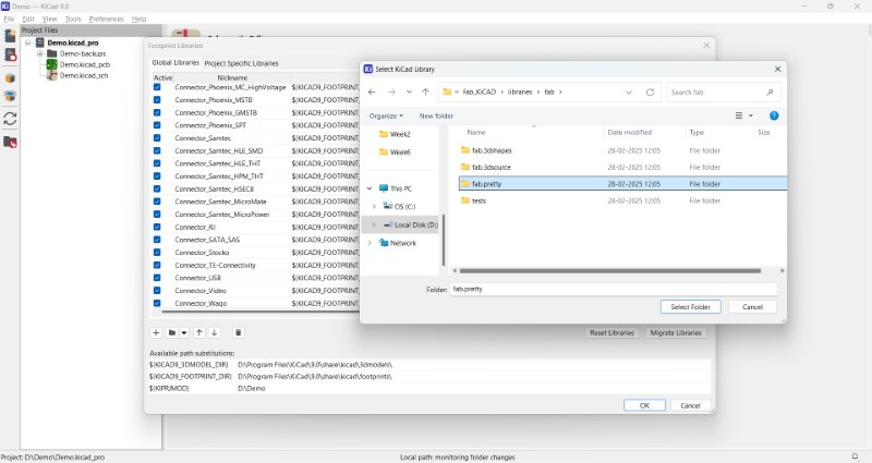
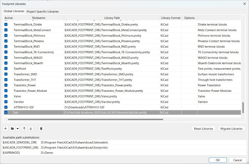
To add footprint folder, go to Preferemces > Manage Footprint Library > Select 'Folder' icon (Add existing library to table)> Select the 'ATTINY412-SSF' Folder > Select 'Ok'
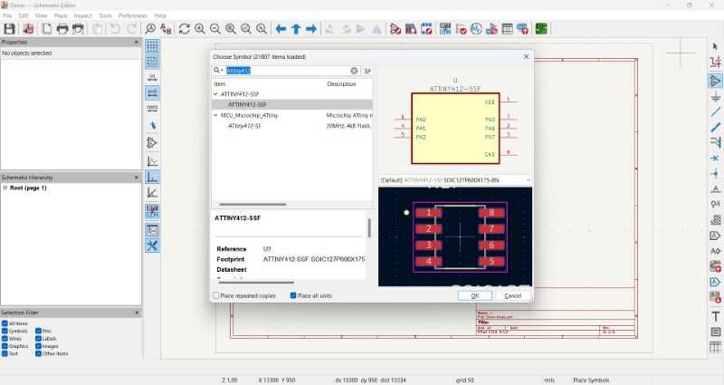
To add the symbol to our schematic, we press the shortcut key 'A', select the desired component and place anywhere inside the page
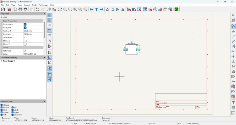
With this I have learned to add symbols and footprints for components not already available to us.
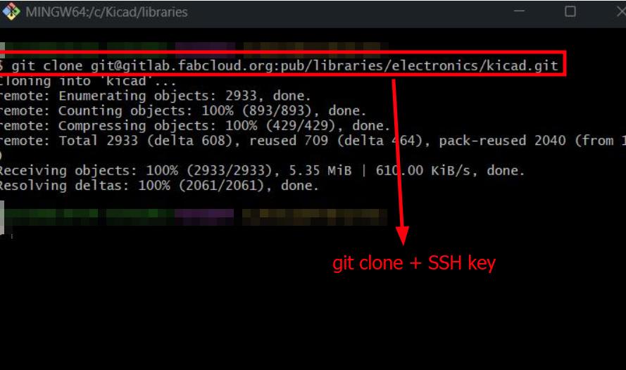
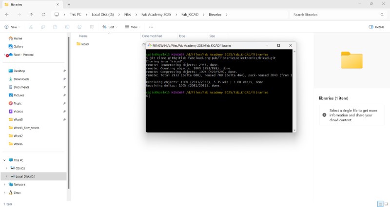
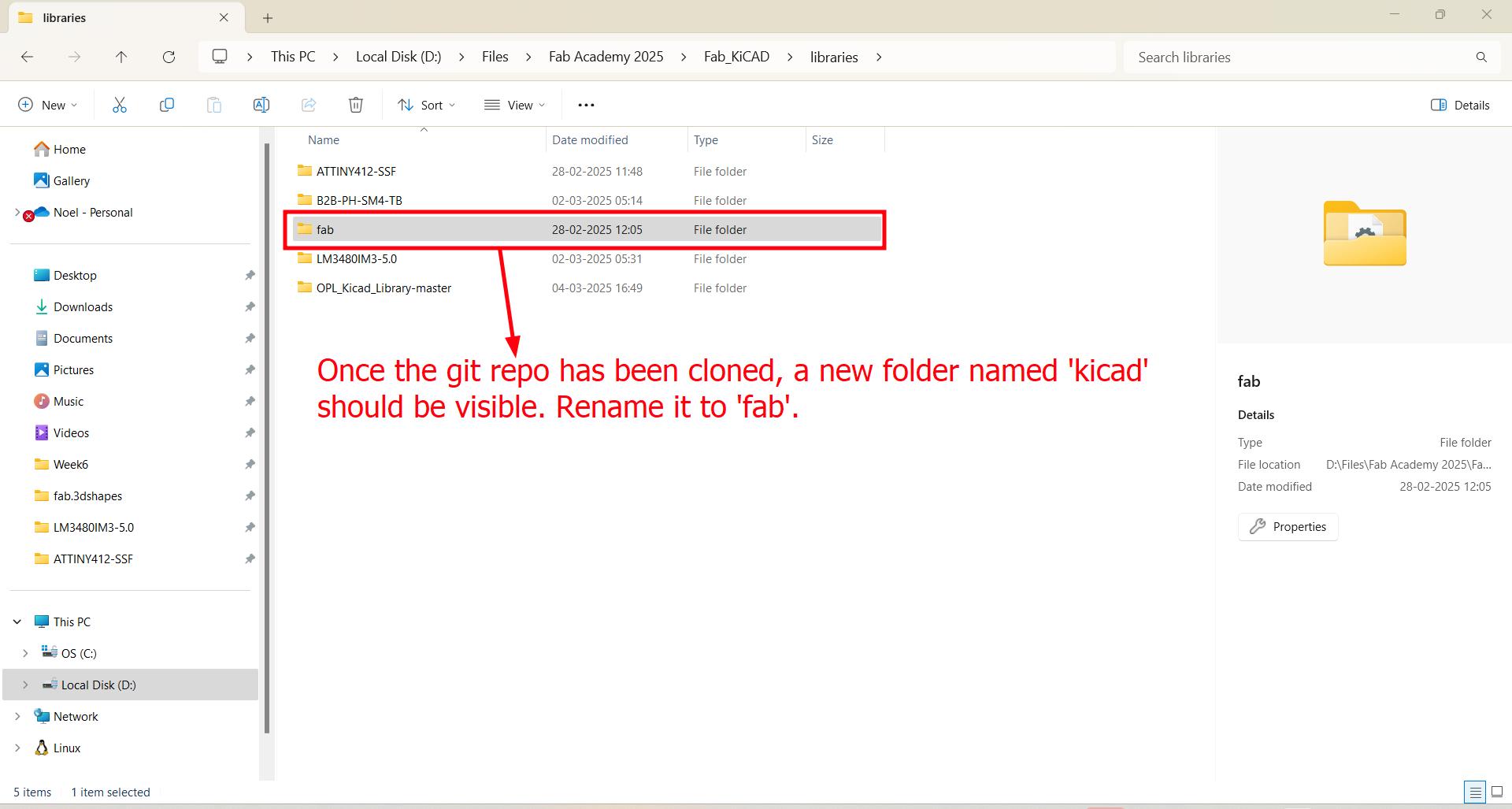
Then I learned to add Fab KiCAD library to the software. For that, I need to clone repo of Fab KiCAD library. First I go to gitlab documentation page. I copied the url that allows me to clone with SSH key, come to the File Explorer, create a folder named 'Fab Academy_KiCAD', make a subfolder named 'libraries' and cloned the repo. I rename 'kicad' folder in library as 'fab'.
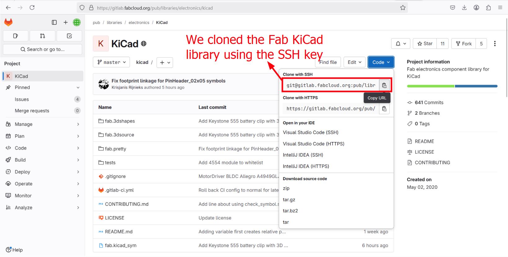
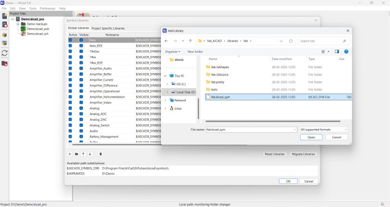
Then just like before, I add symbol and footprint folders to KiCAD.
Schematic Editor
A schematic diagram is a 2D representation of a circuit using standardized symbols showing the functionality and connectivity between different electrical components. It acts as a map while designing, building, and troubleshooting electrical circuits.
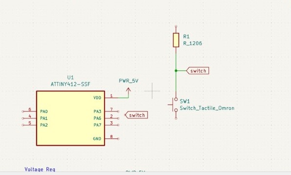
Now I am going to add a 1206 SMD package resistor, a pushbutton switch and then connect them in series to common power line and common ground to make a pull up resistor from the fab KiCAD library. To prevent floating input, I am going to 'pull' it to a logic 'HIGH' state. To move the components easily, the shortcut key M can be used. To rotate by 90 degress, use 'R', To draw connections between components, use 'W'.
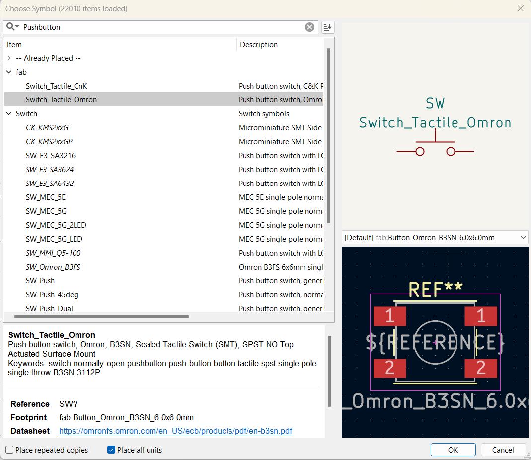
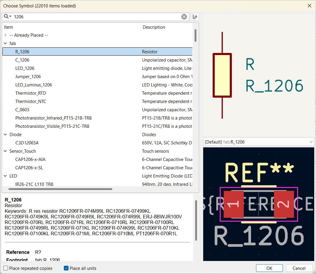
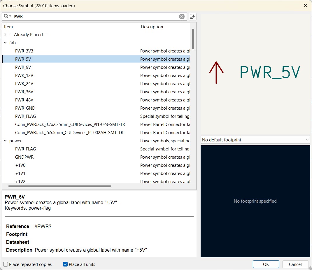
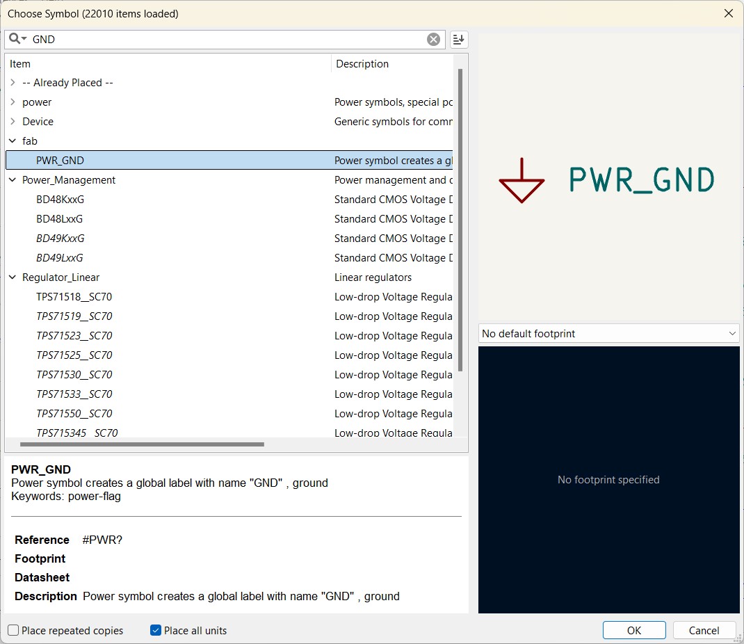
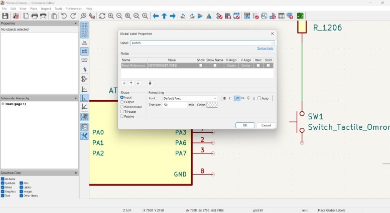
Now I am going to add global labels like 'switch'. Here, two parts of the circuit with 'switch' will be connected to each other.
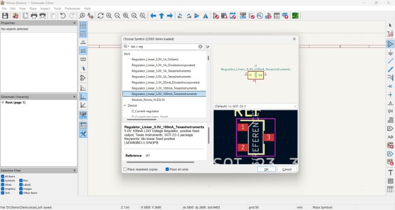
Based on the datasheet, I know the chip can handle 1.8 to 5.5 V, so I added a 5V 100 mA regulator
20-03-2025: I used the help of ChatGPT to understand why two capacitors are required.
Prompt: Why do we need capacitors in parallel with linear regulator?
1. Input Capacitor (Cin)
Function: Stabilizes the power supply before it enters the regulator.
Why needed?
- Filters out noise and fluctuations from the power source.
- Reduces voltage dips due to supply line resistance and inductance.
- Ensures a stable input voltage, preventing oscillations in the regulator.
2. Output Capacitor (Cout)
Function: Maintains a steady voltage at the output and improves transient response.
Why needed?
- Provides charge during sudden load increases (acts as an energy reservoir).
- Reduces voltage ripple and noise at the output.
- Prevents instability and oscillations, especially in low-dropout (LDO) regulators that rely on proper capacitive loading.
Why Not Just One Capacitor?
- If only Cin is used: The regulator might still experience instability due to rapid load changes at the output.
- If only Cout is used: The input voltage might fluctuate, causing improper regulation.
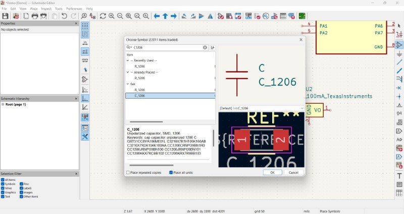
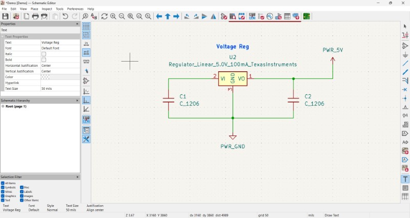
To add text to label each part of the schematic, I use the command T
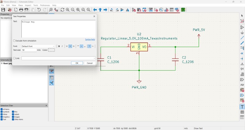
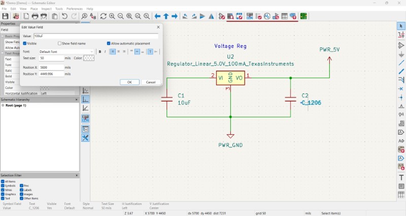
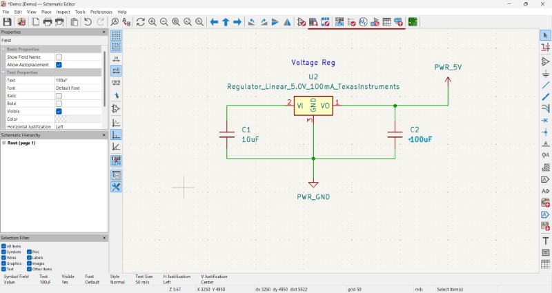
To add values, you simply double click the fields you want to edit
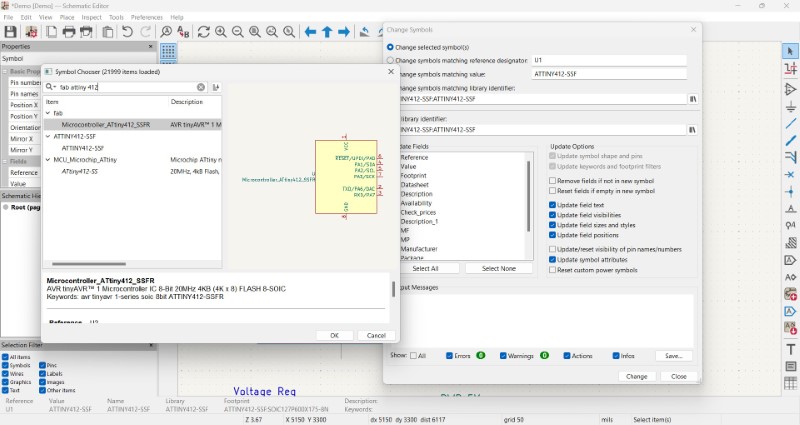
Later we also replaced the symbol with the Fab symbol for ATtiny412
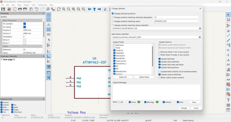
With this I have created a minimum circuit
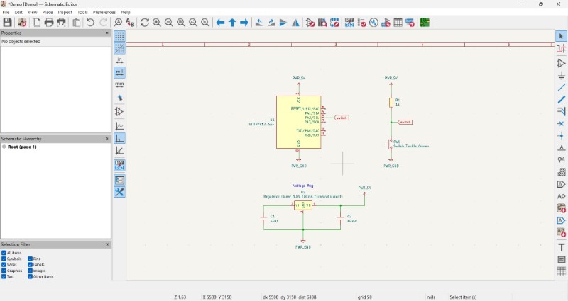
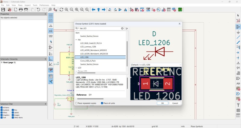
Now I wanted to add two circuits for onboard LEDs, one that can be controlled from one of the digital I/O pins, and the other a power LED
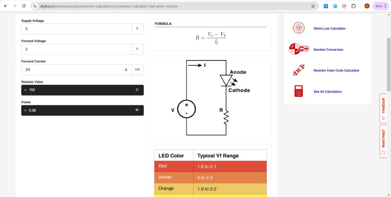
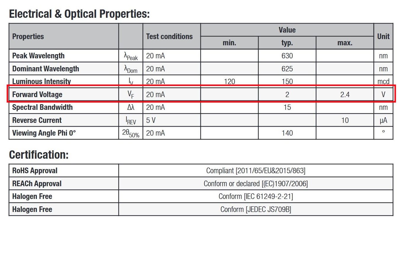
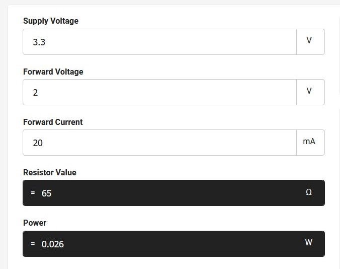
To calculate the value of the resisor, we look at the datasheet and find the relevant forward voltage. current, and also the supply voltage (5V) and input that into the LED resistance calculator to calculate the value of the series resistor that should be added
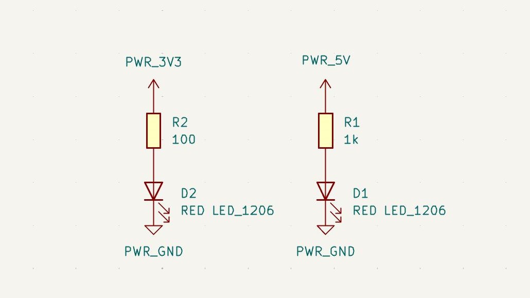
Once I made one circuit, I made another one for an onboard Power LED with increased series resistance value for reduced current draw and reduced brightness as a result
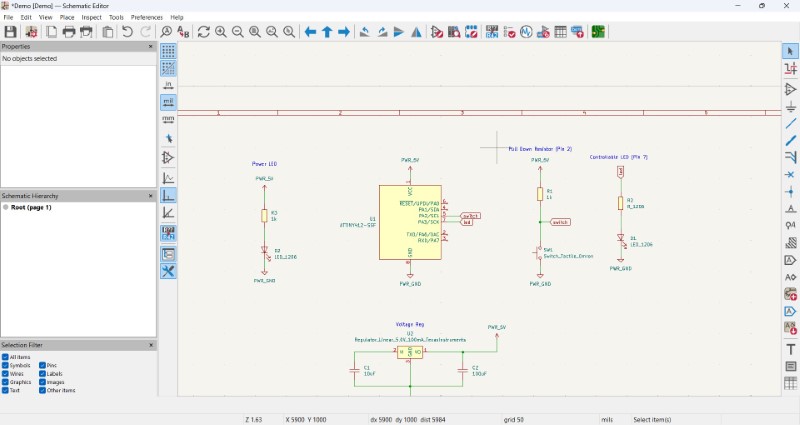
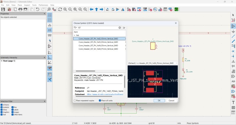
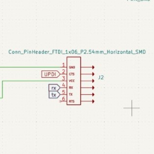
Now I came back to the power supply part of the board. I first add a JST connector, and then a FTDI connection for the programmer and debugger. VCC and VDD denotes positive power supply for digital and analog circuits respectively.
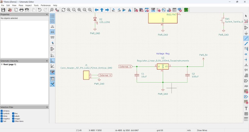
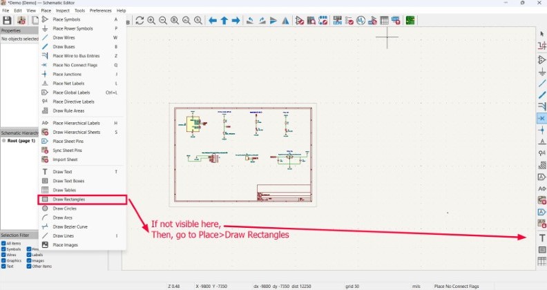
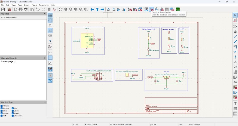
The tx and rx are switched in header FTDI. I then added 'No Connect' Flags to unconnected pins. Also I drew rectangles to keep the schematic neat & tidy
Electric Rules Checker
I then used the Electric Rules Checker to check for and correct errors
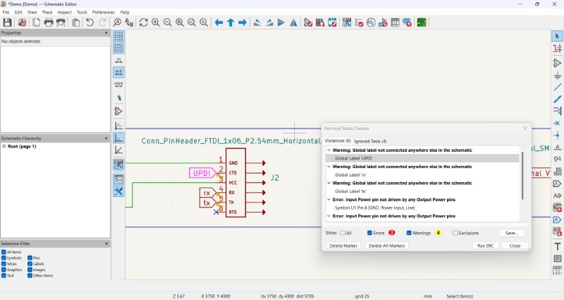
I corrected warnings related to UPDI, tx, and rx global labels.
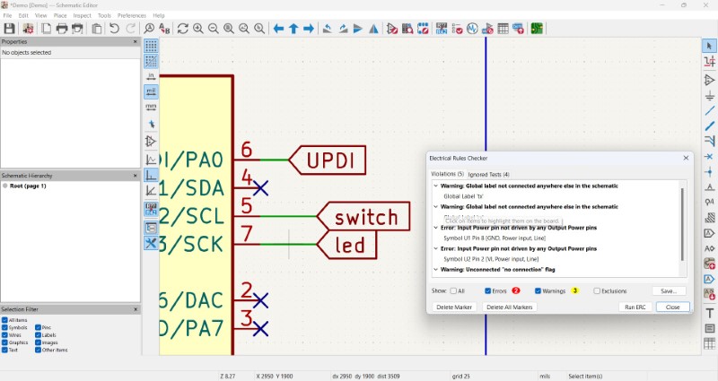
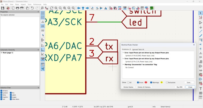
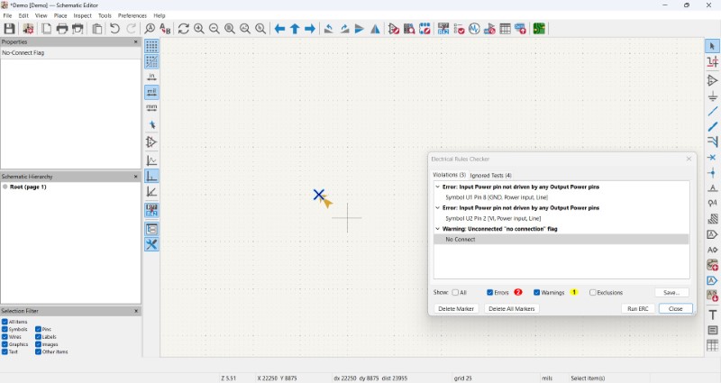
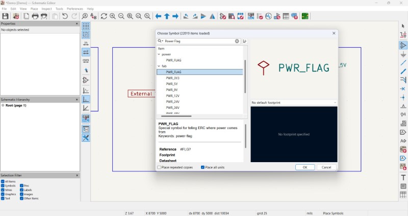
I also corrected warnings related to 'no connection' flags. PWR flags are given to tell the software to consider them as power inputs/outputs. In this way the other two errors were solved
PCB Editor
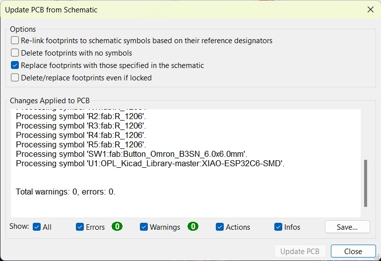
Now we have cleared all the warnings and errors, so we move away from the Schematic Editor to PCB Editor. First I update schematic to bring in PCB components from Schematic Editor
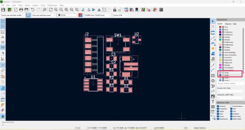
To disable all text components to be able to reduce the clutter while arranging we disable F Fab and B Fab
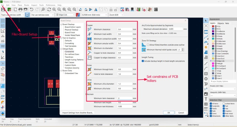
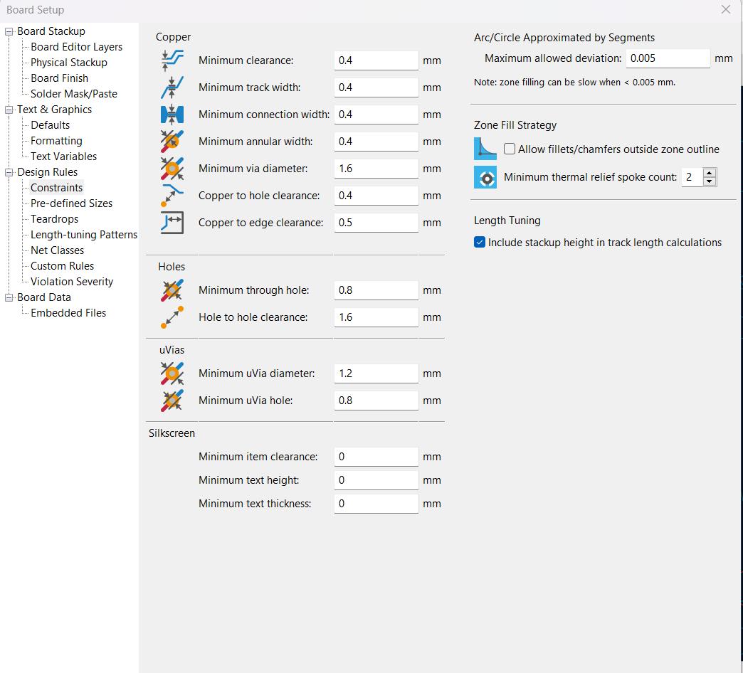
Now we update the constraints based on our milling machine. The values were provided by our instructor
Now we need to place each component in such a way to reduce the number of knotted airwires. To see which component is which, I select, and then Alt Tab to switch between selected PCB component. The pins on FTDI and the JST connectors should always face outside away from the center of the board.
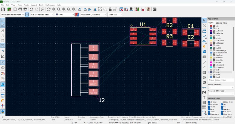
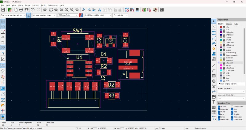
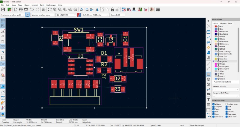
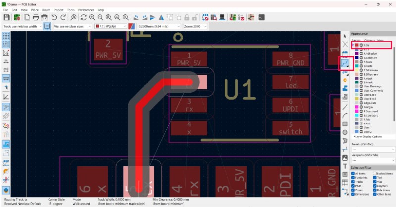
Once placement is done, I draw a edge cut rectangle path (White colour). Once done, its time to draw traces. I select F Cu and draw traces using X command.
Some tips to to be followed while making traces
- Only traces for ground and power at the last, after all other connections have been made.
- You can draw traces in between resistors
- Avoid 90 degrees in traces, add cruves using D command
- Using tilde key to see all connections of one terminal
- Using D to edit traced paths
- Unroute selected to remove entire traced path
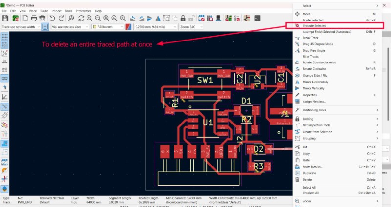
Design Rules Checker
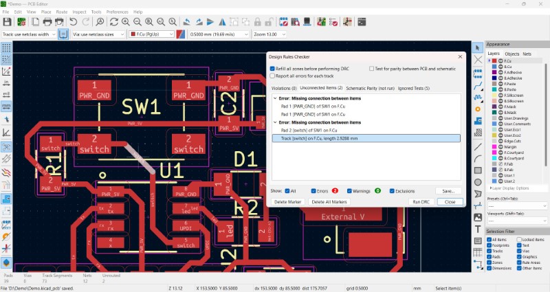
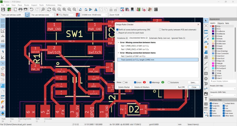
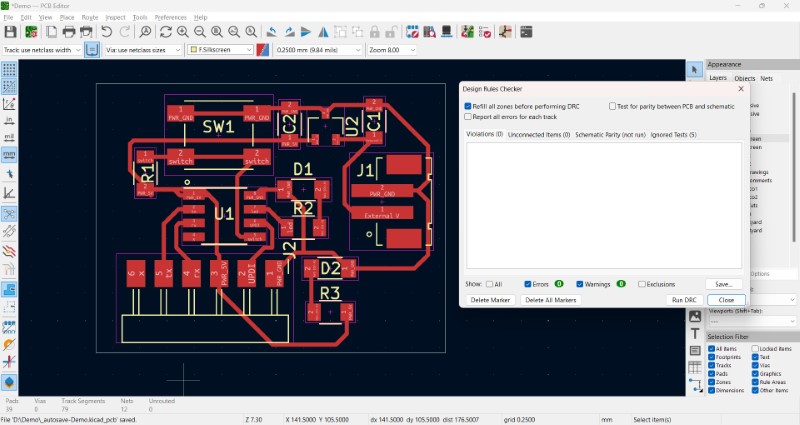
Once done, press Design Rules Checker to understand if you have made any errors including any missing connections. While I did not get any errors of this kind initially, I did get them later once I modified the design.
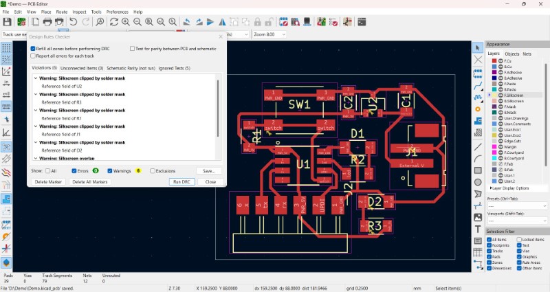
Instead I got errors related to labels being clipped by traced path. Later I got an error due to an unconnected end while moving components
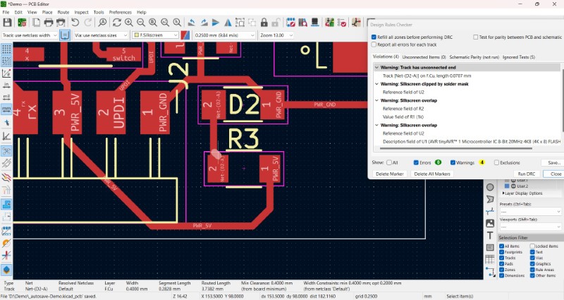
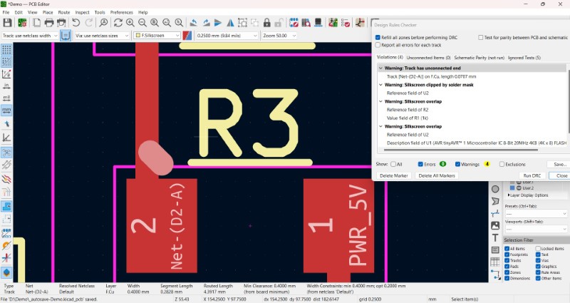
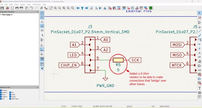
You can use a 0 ohm resistor like a highway bridge when there is no space to make traces. I also got errors related to traces in the switches. These can be ignored since they are connected internally, but I choose to make traces regardless to clear the errors in the dialog box.
3D Modelling
Once I cleared all the errors in the Design Checker I can now go onto the third part of the designing process; add 3D models. Since the links are broken we will need to manually relink the file paths of the STEP files under 3D models
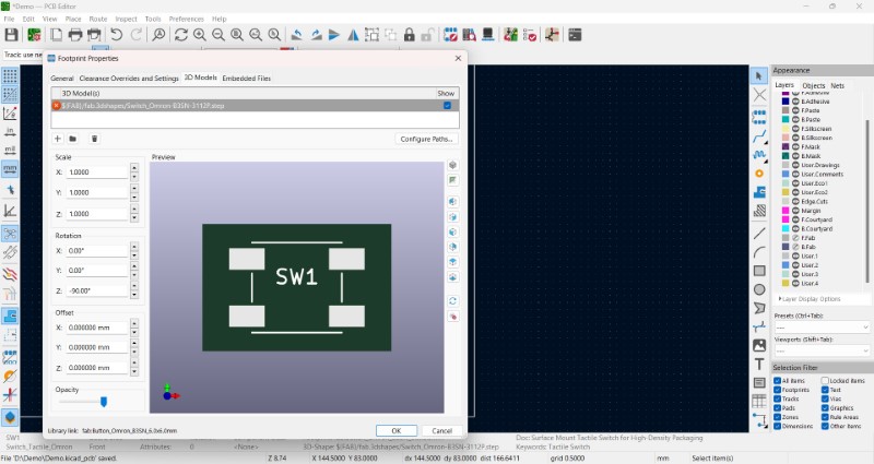
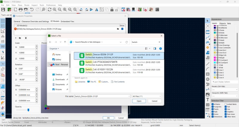
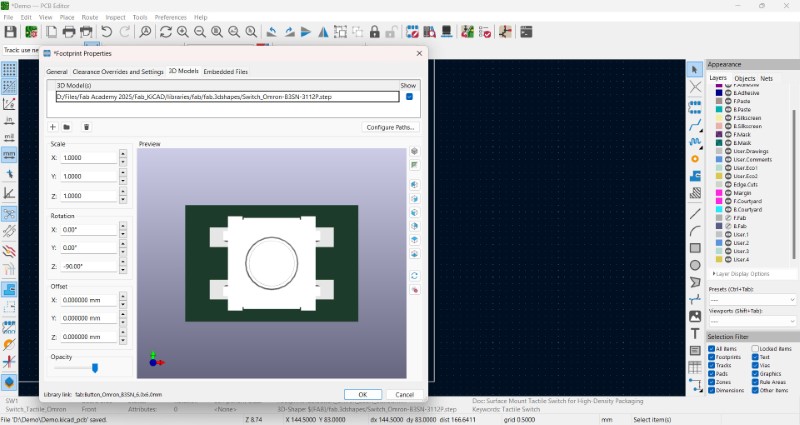
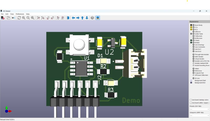
On sucessful relinking, you will be able to see the 3D model in the preview window. You can use the Shortcut Alt + 3 to go to the 3D viwer to see the entire board in 3D. Even though the STEP files for each SMD resistor or capacitor is the same, you need to relink all of them individually, which I found a bit inconvenient. As you can see above the 3D models of the Voltage regulator and the JST connector do not exist in the Fab KiCAD library, so they have to be imported from an external source, just like before
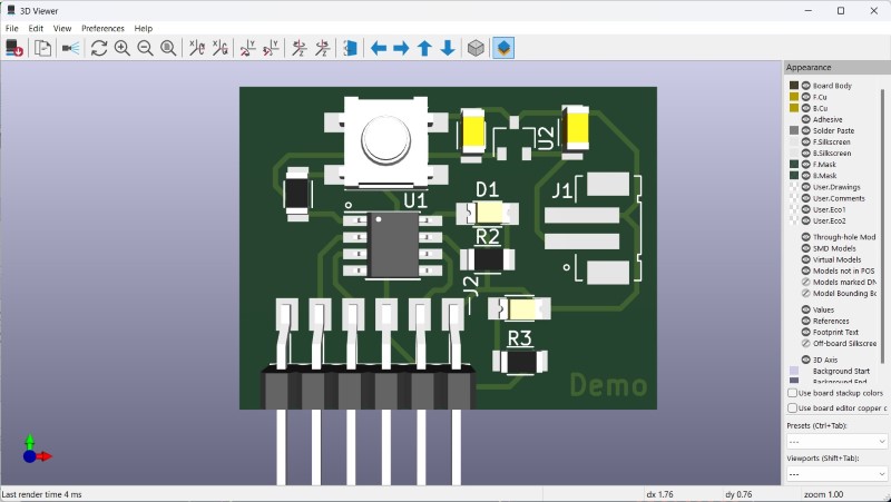
02-03-2025: So I went back to the schematic editor and copied the name of the JST connector component. I wasnt able to get the required search result on copy pasting the exact name as is. I tried changing the name multiple times but to no avail. So I decided to try with matching the part number instead.
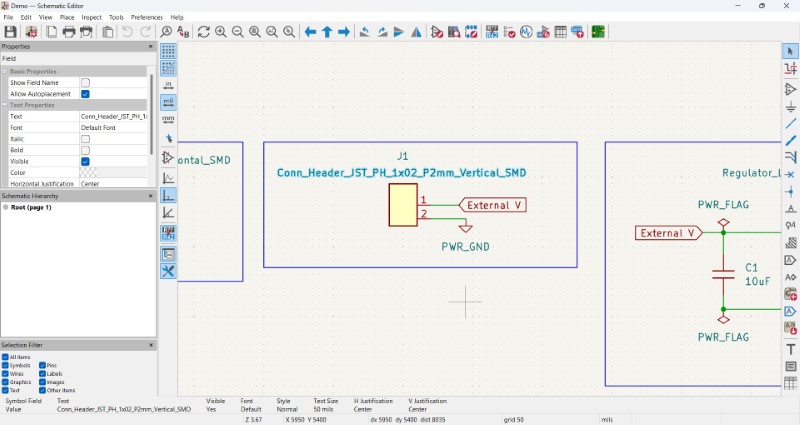

It took some time to figure it out, but I was able to find the model number and get a match for it in Snap Magic
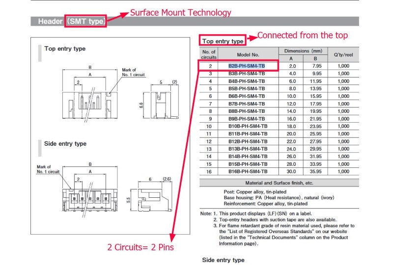
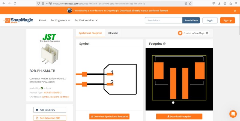
I downloaded the zip file of both the symbol and footprint and followed the same steps just like how I did for ATtiny412.At first I tried changing just the 3D model and nothing else, but that did not work. So I decided to change the footprint folder and see if that would work. It works better than just using the 3D model, but im not sure that it is perfectly aligned, but for now it will do.
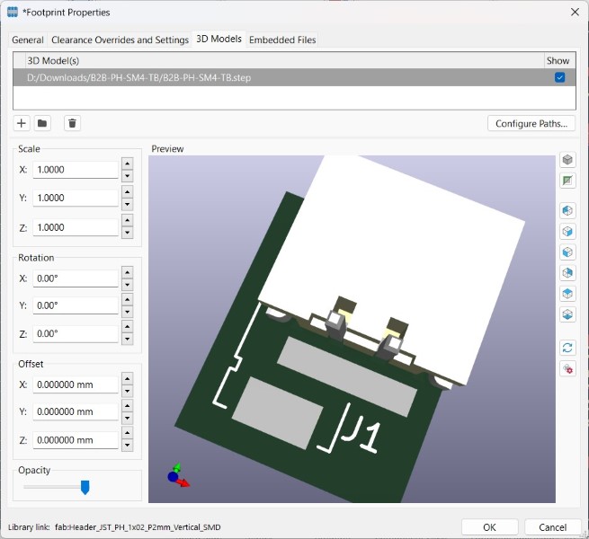
I had only later noticed that changing the footprint also changed the orientation and removed the trace connections to the part, so we had to add connections to it. I unrouted some selected traces and used the tilde key to highlight all the pieces to be connected by traces. Then I made new traces for the same.I also ran the Design Rules Checker (DRC) and corrected minor issues with the silkscreen labellings which won't be printed anyway. I repeated the process for the voltage regulator, but this time I only downloaded the footprint folder including the STEP file.
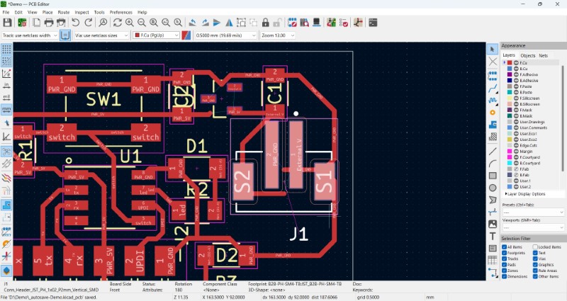
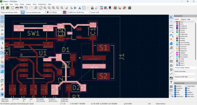
Once done I thought my CAD model was complete but there was an issue. The orientation of both these components looked wrong. Then I replaced both the symbols and footprints, which also did not work.
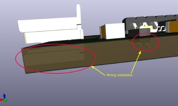
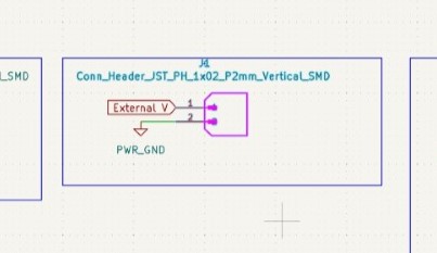
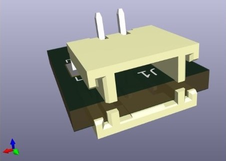
It was getting very late, so I will stop this for now and consult with my instructor on Monday.
03-03-2025: My instructor showed me how to rotate the models in KiCAD itself. I was a bit embarassed by how simple the solution was. I rotated both the JST connector and the voltage regulator
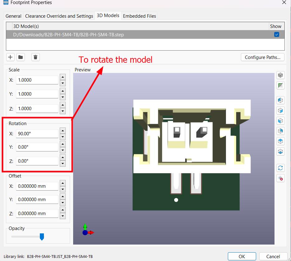
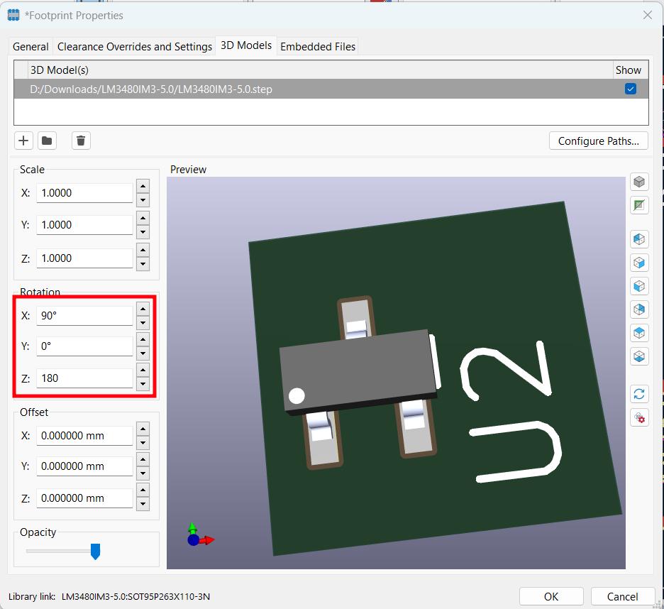
This is how my demo board looks like completed
Common Electronic Components
I have included details on different electronic components discussed in class and available in our lab
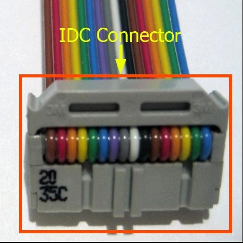
Ribbon Cable: Made of up of several flexible wires running in parallel. They are widely used in computers andd other electronics applications where space is limited.
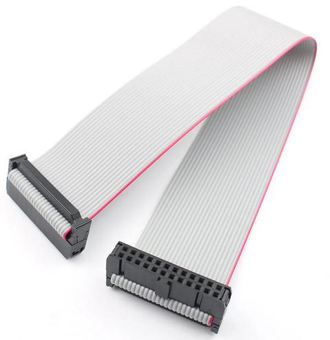
IDC Connectors: Abbreviation for Insulated Displacement Contact, is a wire to board connector that helps create strong connections by piercing the insulation and creating contact points between the wire and the metal contact.
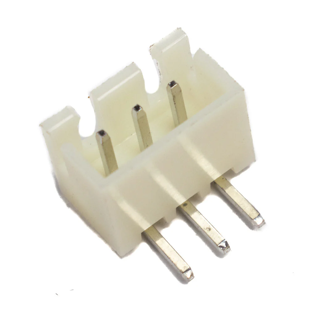
JST Connectors: Short for Japanese Solderless Terminal, another type of wire-board connectors
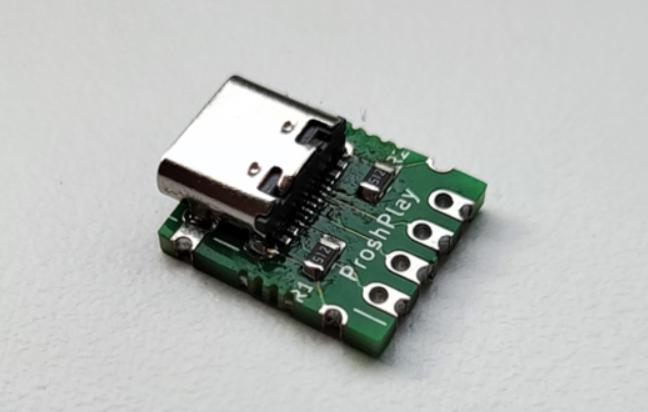
USB Connectors: Short for Universal Serial Bus interface standard . The USB standard was developed to simplify communication betweeen a computer and multiple different peripherals. The following image from PCBway shows us the wide variety of USB connections available. The following breakout board was made by our instructor, Saheen Palayi for the purpose of connecting to USB C cables easily.
Pushbutton switch: A device used to establish new or disconnect previously made connectiosn with another device
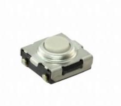
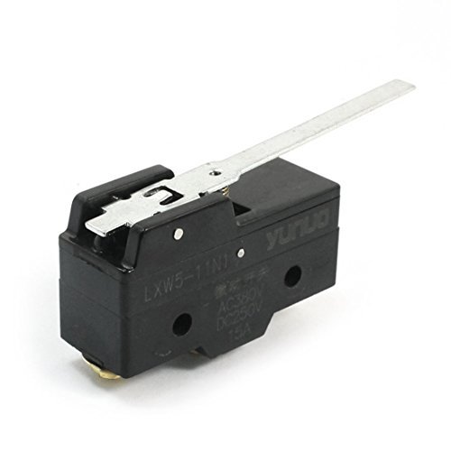
Limit Switch: A limit switch operates by the motion of a machine part.
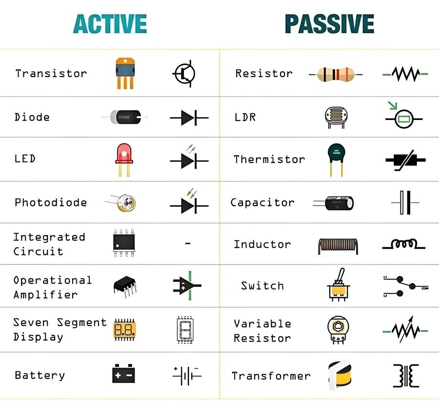
A resistor 'resists' the flow of current.
A transistor is a miniature semiconductor capable of controlling voltage or current flow in electronic signals and is also able to amplify and act as a switch for them. The most common types of transistors we use today are MOSFETs.
A capacitor is made of two conductive plates held close to but not in contact each other, which causes it to to act 'like' a battery, ie. it is able to store charge. But unlike a battery, it cannot store the charge for a long time, instead the electrical energy it stores is instantaneously dissipated into the circuit when there is no currrent flowing.
A diode is a semiconductor that essentially acts as a one way switch, allowing current to pass through in one direction, but blocking it from coming through the opposite direction. We mainly use germanium diodes
An LED is a light emitting diode, which emits light when current flows through one direction. LEDs must be connected in series in any circuit to allow it from blowing out due to accidentally reversig the polarity.
Individual Assignment
03-03-2025: For the purpose of our assignment, I am going to design a development board using the Seeed Studio XIAO ESP32C6. I am using Adrian Torres' documentation for reference while building my board
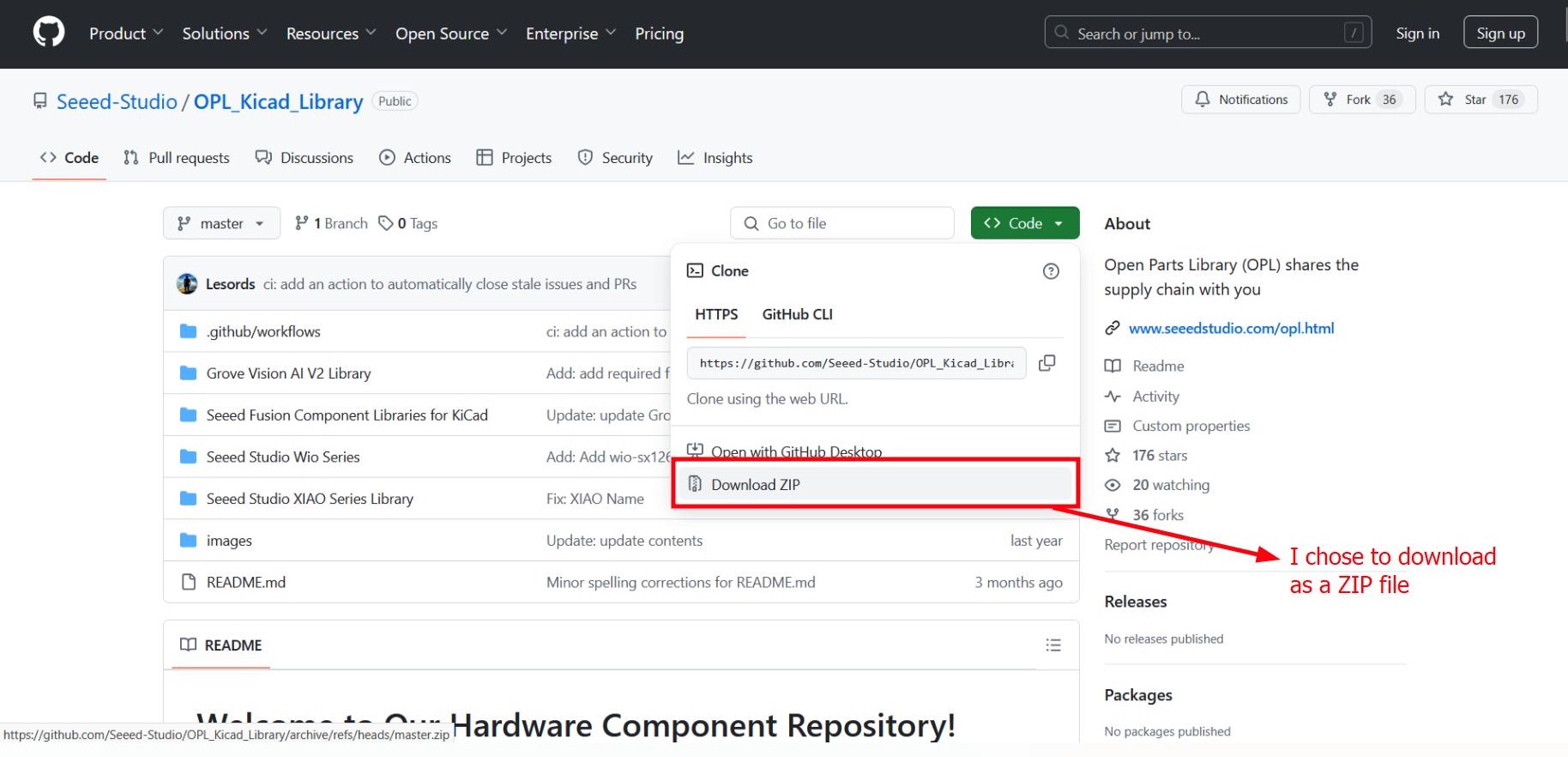
This is the github link to the libraries for the Seeed Studio OPL_KiCAD Library. I downloaded as a ZIP folder
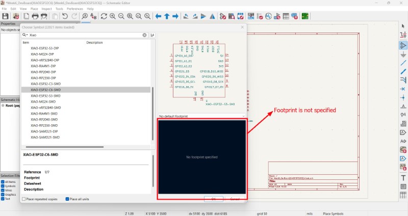
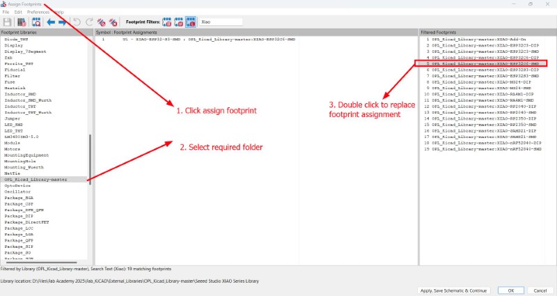
When adding the symbol for the MCU, you will see that it says no footprint specified.So I assigned footprints for it, click 'Apply' and select 'Ok
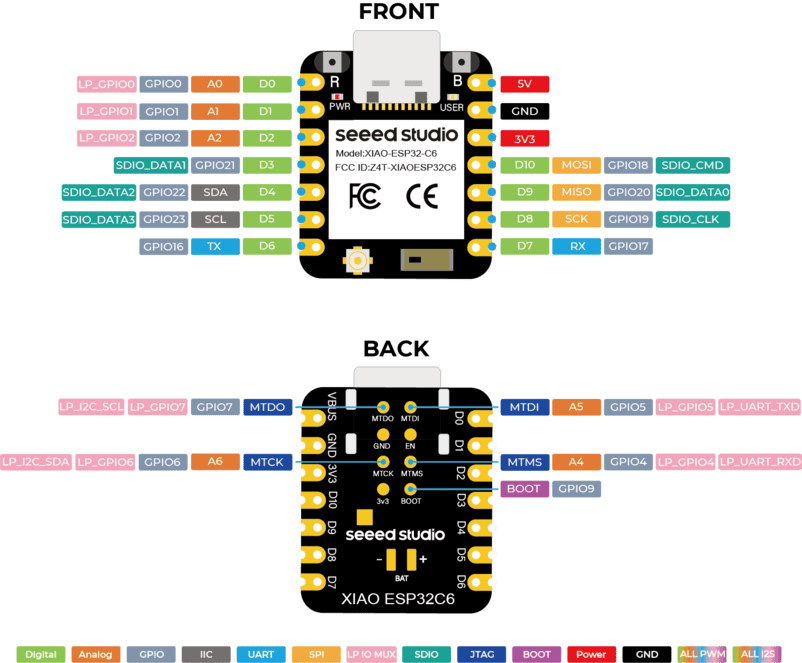
This is the pinout of XIAO ESP32C6
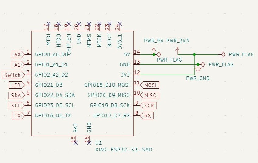
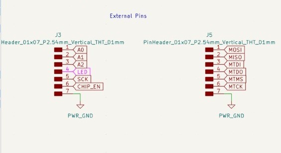
First I added global pins for many of the pins, and connections to GND for pin 13 and 3/5V for pins 12 and 14 respectively.Then I added connections from a pin header row to PWR and GND. The Serial Clock Pin (SCL) and the Serial Data Pin (SDC) pins are used in I2C protocol. The SCL pin sets the speed of data transfer, while SDC pin tranfers the data. An example where I2C is used is in OLED screens. You can read more about I2C protocol here.I got some instructor feedback saying I need PWR and GND connections for both UART (TX and RX pins) and I2C. Also the UART pins ideally should be horizontal, so I made those changes. Then I added vertical through hole header pins for all the external pins that are not already connected to some header pins.
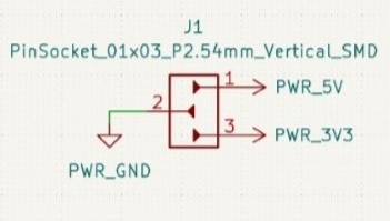
Now we add a Power LED for each voltage source to confirm that 3V and 5V power supply is working properly. To figure out the value of external resistor, we go to the datasheet and input the values in the LED resistance calculator. The minimum required resistance is 65 Ohm for a 3.3 V supply. I will be using a 100 Ohms resistor here, since that is the closest value of resistor we have here that is also greater than the required minimum resistance.
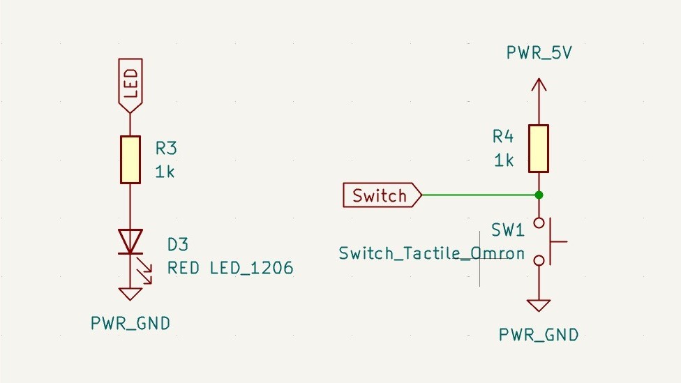
Then I added a controllable LED and switch connected to GPIO 21 and GPIO 2 respectively. I then added rectangles around them and click on Electric Rules Checker and corrected the errors I found
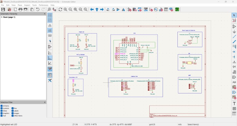
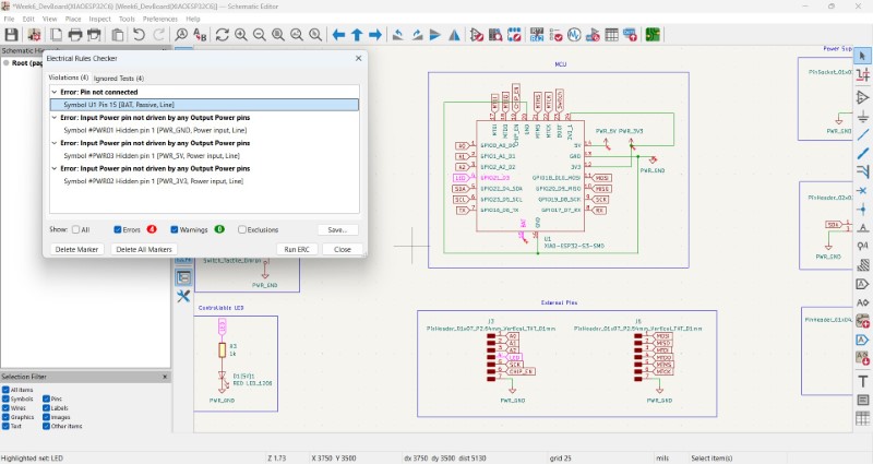
Now I go to the PCB editor. When updating the schematic, I got this error. So I went back to the Schematic Editor and assigned a footprint. Now it works and im able to get all my component footprints in the PCB editor.

For now I am stopping here. I will continue this tomorrow morning.
04-03-2025: I continued from where I left off yesterday. First I, changed the through hole header pins to SMD Pin Sockets since I will be plugging components into these sockets and I will be using only SMD components. Later I found out that a 1x07 2.53 Pin Socket already exists in KiCAD native library. If I have to edit the footprint, I have to edit it by clicking on the option in the Schematic Editor itself.
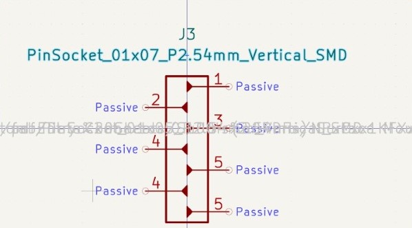
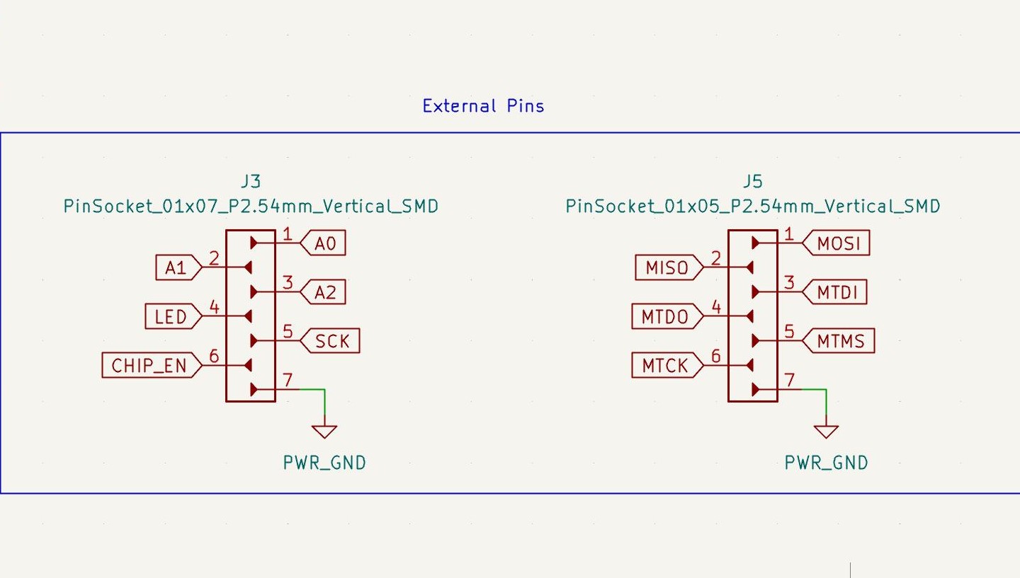
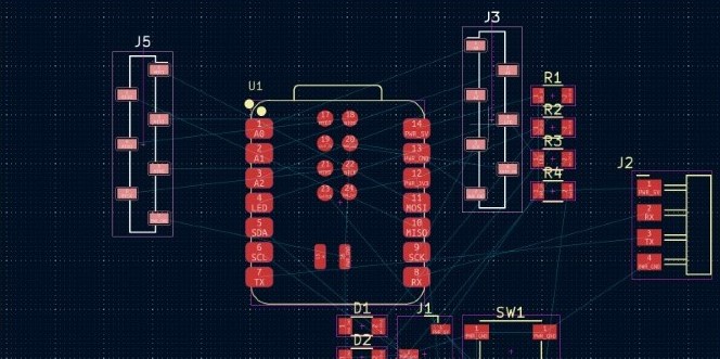
I have arranged all the components to fall into a box of maximum dimensions 80x50mm. To reduce tangling, I have swapped pins in header pins. This is how it looks like before tracing. I used the following constraints for tracing.
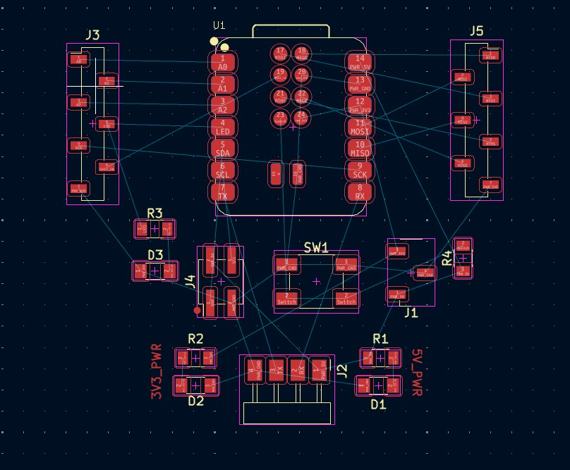

I used a 0 Ohm resistor when I needed to make connections over other traces.
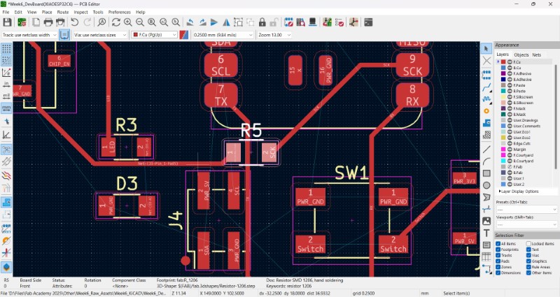
I was informed that none of the pins below the board were required so I proceeded to delete them
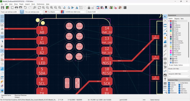
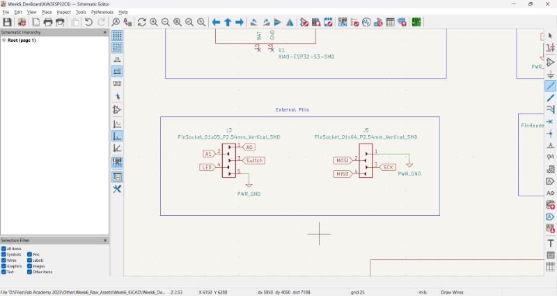
After multiple attempts, I was finally able to trace all the connections. Based on some general advice given by instructors in Local Review, I also made edge cuts to the PCB to expose the USB port for thicker cables. This is what the final schematic and PCB looks like
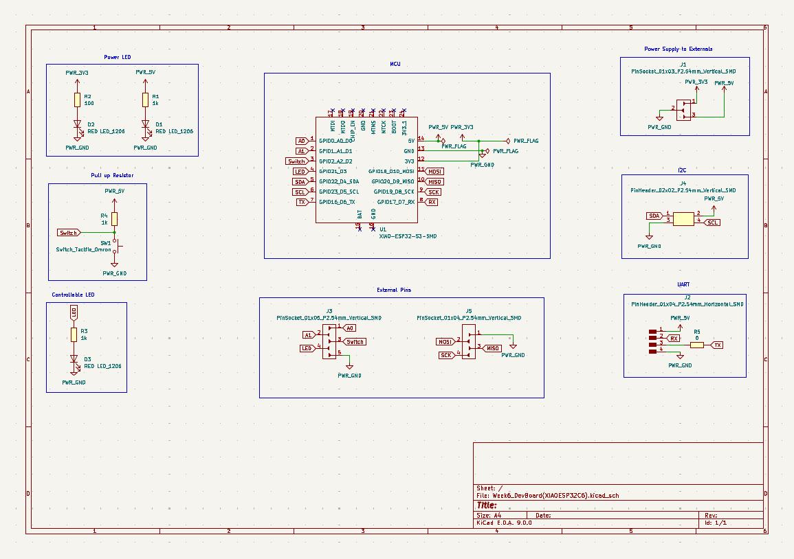
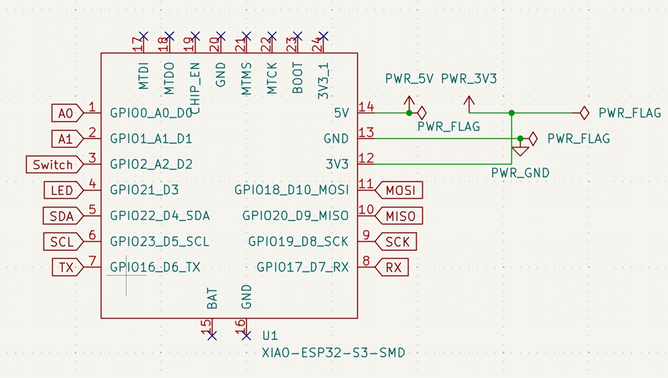
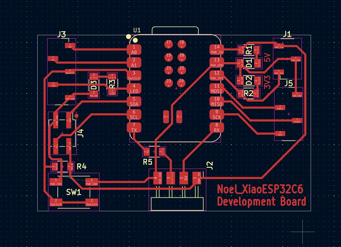
I ran the Design Rule Checker and corrected all the errors. Warnings related to clipped silscreen have been ignored since we are not going to be applying it, and errors related to missing connections between the two switch and two PWR_GND terminals are going to be ignored since they will be connected once I add the pushbutton switch component
For Seeed Studio Xiao ESP32c6 can be obtained from GrabCAD. I then brought into the 3d viewer, adjusted the angles and the offset to get it into position.

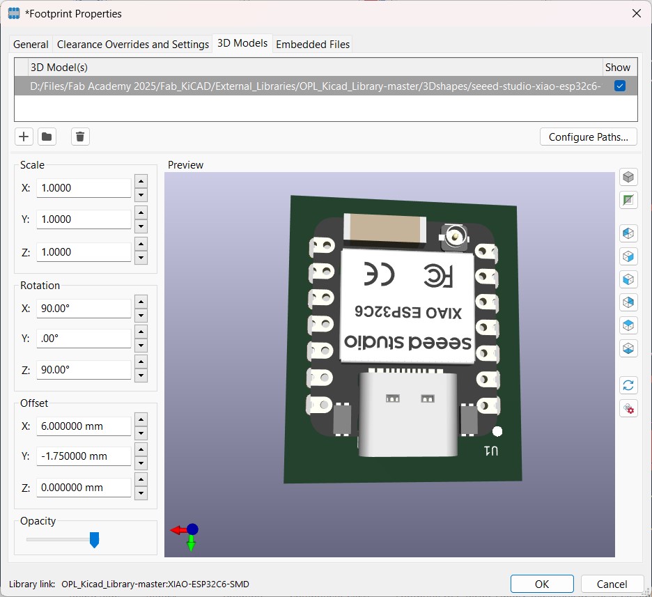
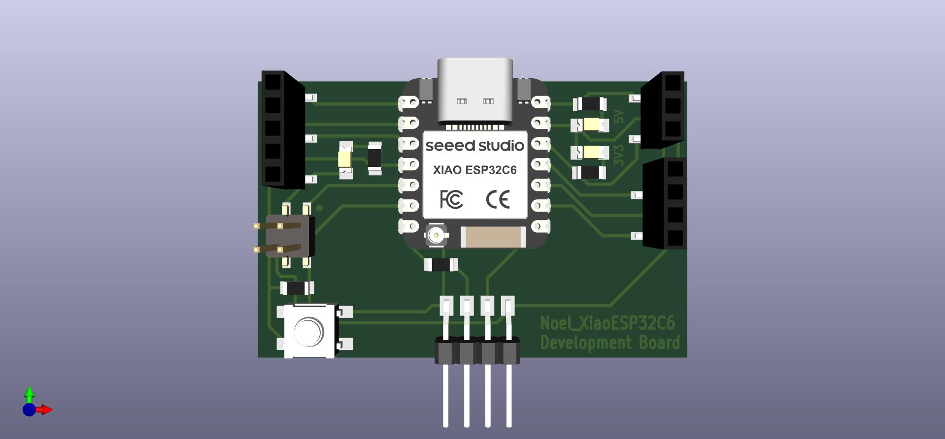
This is how the final output looks like:

Final Project Work
02-03-2025: Now that I have some basic idea of how to use KiCAD, I wanted to make a development board for my final project. This Youtube video by Robonyxfeeaturing the building of a self balancing robot with an expressive display was very impressive and I wanted to incorporate the wheels and the self balancing into my design, In the build, they used an ESP32-DevKitC, and since I did not enough of an idea of the specifics, I decided to build my board base on this design.
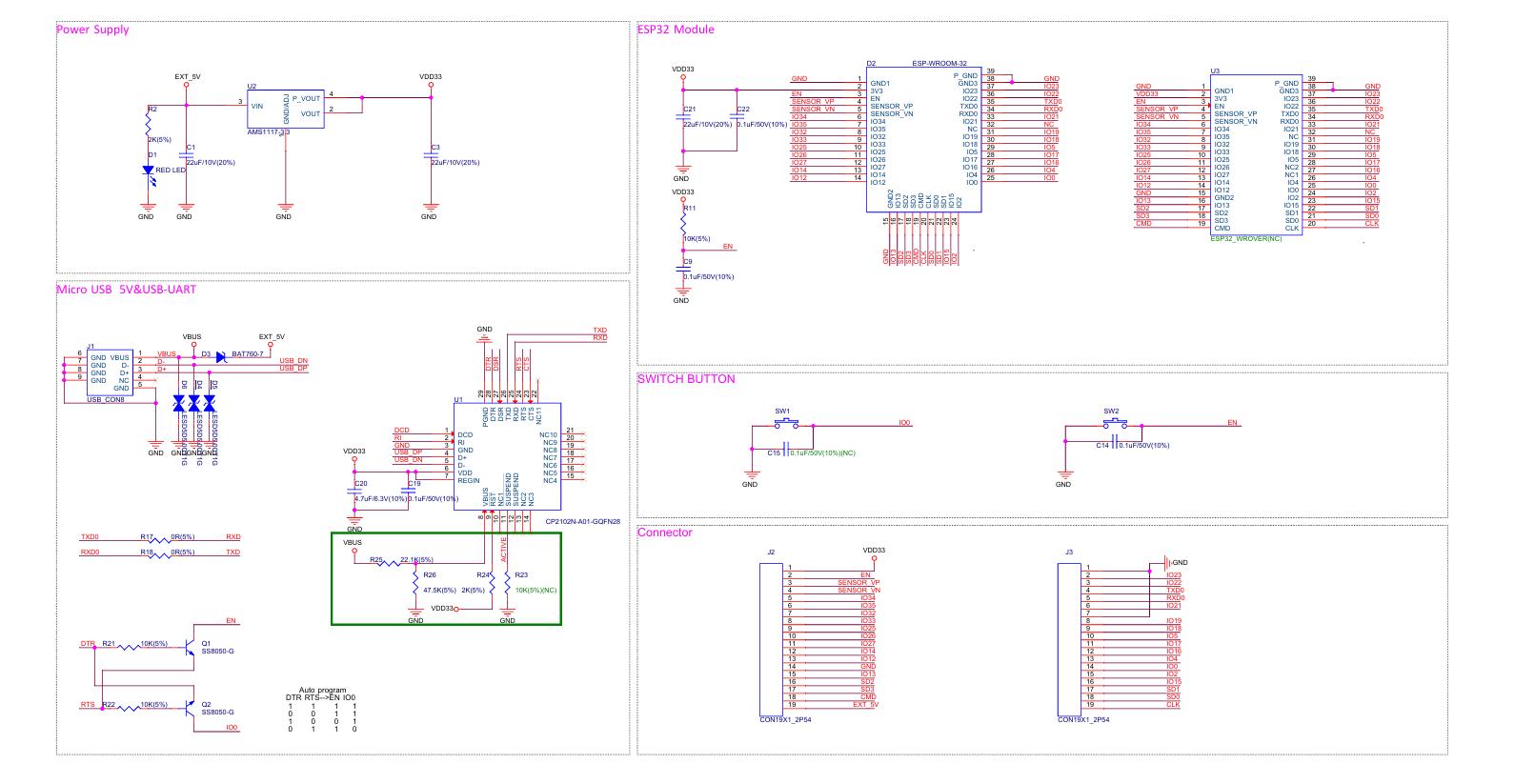
Then I crosschecked that the ESP32-WROOM-32E module is available through our lab's inventory site. I am not sure if this is the exact same module that was used, but I am going to wing it for now and figure it out as I go.
Since I have no background at all in this subject, I am using the help of this instructable to build a basic development board with at least the most important parts. The article was prepared for the 'Clouduino Stratus' development board using the ESP8266, so some things will be modified in my design. Now we start designing
So we open KiCAD as before and add a symbol for the ESP32-WROOM-32E. I cross checked betweeen the datasheets of the component in the fab KiCAD library and our inventory to confirm that I am using the correct symbol.
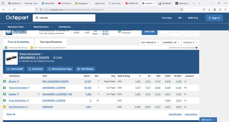
The datasheet mentions that the typical operating conditions of this MCU is 3.3 V and 500 mA, so our regulator needs to match these conditions. For our purposes I use the LM3480 which is currently not listed in the inventory, so I used Octopart search engine to find out more about their availability. I then followed what I did before and made a Voltage Regulator Circuit with the same capacitor values I used for the Demo PCB schematic.
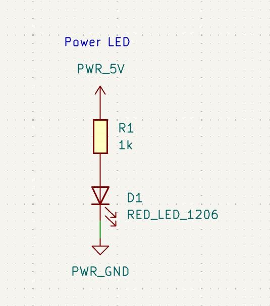
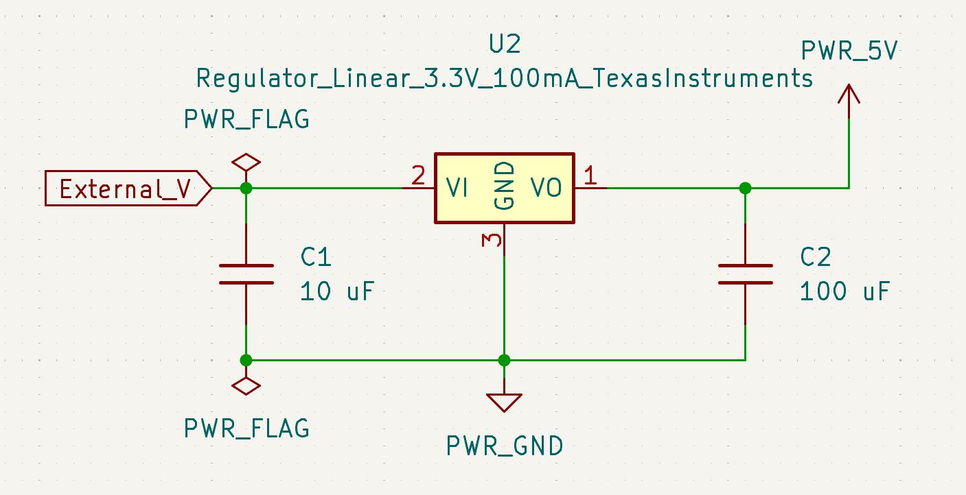
I then added a circuit for a Red Power LED just like before and added text labels. Since the calculation for the resistor was done before itself while making the demo, I will not be repeating it.
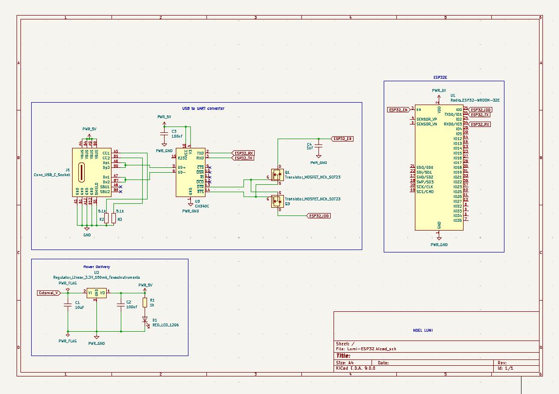
I need to make a USB C type to UART converter using the CH340 which is currently available in our lab, but I didn't understand so I split the USB to Serial interface into two parts:
- CH340C to ESP32: For this, I will use the help of this article I found that listed how to write to ESP 32 from a micro USB
- USB (C) type to CH340 C: For this part, I will use the help of Sparkfun USB(C)-to-Serial adapter based on CH340C IC
1.CH340C to ESP32
To make this part of the circuit, I am using Kohacraft's schematic
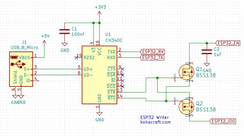
Pins of CH340 have been listed here (extracted from the datasheet)
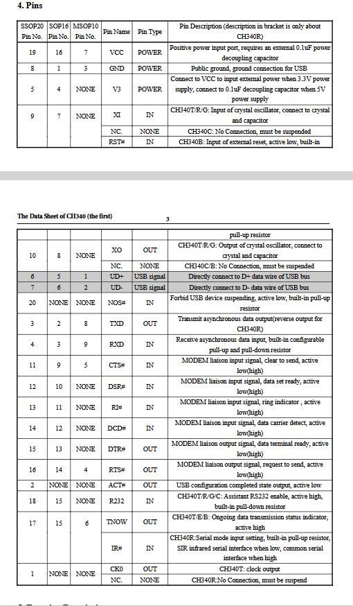
Pin 16 and 4 will be connected to 5V supply in combination with a 100nF (or 0.1uF) capacitor. According to decoupling capacitorsconnect between the power source and ground
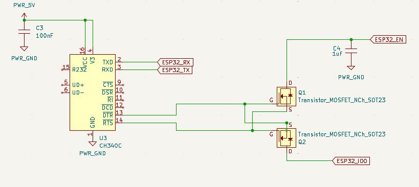
Pin 13 stands for Data Terminal Ready (DTR), which provides a signal to the modem that the server(?) is ready to recieve a connection.Pin 14 stands for Ready To Send (RTS), which meanswhen the pin is set to HIGH, the system instructs the modem to send or receive data, and when it is set to LOW, it instructs the modem to stop sending data.
In the example shown, they are using a BSS138 MOSFET (an N channel MOSFET). We do not have this specific type, instead we have NDS355AN and AO3400 MOSFETs available. I have chosen these two since they are N-type and have the same SOT23 package, which is a surface mount package for transistors, diodes, and voltage regulators.. Based on my reading, SOT23-3 and SOT23 have the same dimensions. I have chosen the NDS355AN for my schematic since I the symbol is available in fab KiCAD library
Both pin 13 and 14 are connected to MOSFETS, both connected to the gate (G) or the source (S) terminals of each MOSFET. The Drain (D) terminals of each MOSFET should be connected to Enable Pin (Pin 3) or GPIO0 (Pin 25) of the MCU respectively
This is how my schematic looks like now. one concern I have is that I think I am only able to write and not debug with my current connections.
2.USB(C) to CH340C
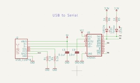
I found the schematic of SparkFun Serial Basic CH340C Breakout Board. A point of note is some connections of the CH340C, eg; Pin 4, are different from Kohacraft's design. I currently do not have the knowledge to asses which is better, so I'll ask about it to the instructor tomorrow.
There are two options for USB_C, both with different number of pins. Based on the pins in the Sparkfun's design and another Breakout board made by my instructor, I took a guess that the option 'Conn_USB_C_Socket' was the correct option to choose.
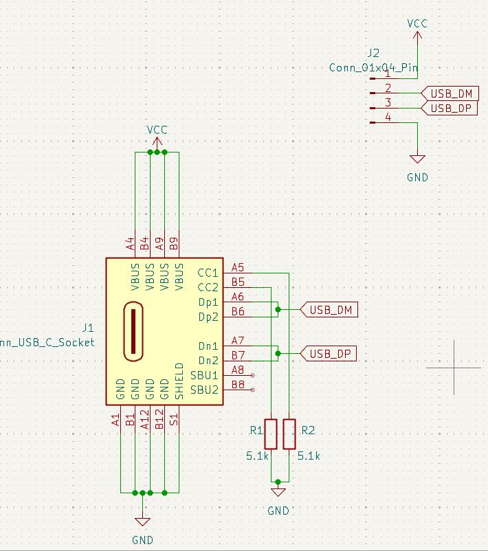
Didnt really understand the documentation for this symbol, so I just followed Saheens example and connected Dp1 and Dp2 as D+, and Dm1 and Dm2 as D-
I will be stopping with this for now. I'll continue with this later today.
03-03-2025: I was reminded to first look for a minimum circuit for the MCU. Then, I have to define the features and then make the board to satisfy those requirements.
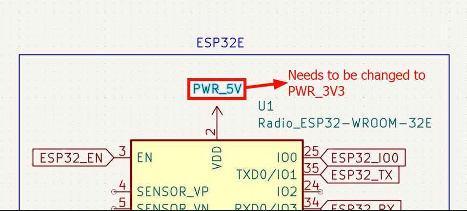
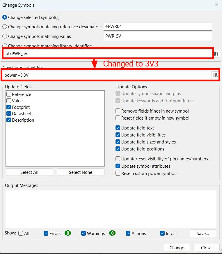
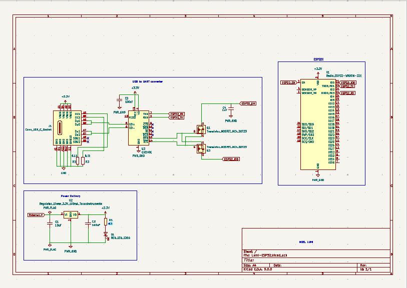
I realized the power symbol added should be 3.3 V and not 5V, so I proceeded to change all of them. Since 3.3 V was not included in Fab library (closest is 3V), I added a 3.3 V symbol from the native library but changing them did not work, so I manually replaced all of the PWR symbols.
In the schematic a 22uF/10V capacitor is used that we do not have in our inventory. Ideally we should the capacitance of an alternative should not change
For now I am stopping here. Right now theoretically, there is a voltage regulator circuit making sure that the MCU receives only 3.3V. Also I can communicate with my MCU using a USB A to C type connector. I will continue to refine this design as the weeks progress.
Conclusion
This week we learnt the basics of electronic CAD. I learnt to use various testing instruments and KiCAD to design PCBs for my projects.