This page will showcase the process and development stages towards my final project.
Presentation Slide
The slide was created in canva . The render of the model was done in fusion 360. I wanted the look of the slide
to have the the aesthetics of retro 8/16 bit game font and styles.
Many nice graphic elements were available in the canva library such as the iconography and speech bubbles of
games.
Presentation Video
This is a rough teaser video to act as the placeholder until the final video is done. Again here too, i wanted
the retro/arcade game aethic to be present throughout. i am still trying to figure out the structure of the entire
video.
The video was edited in can . Under the video category in canva there were many motion graphic templates
available under the retro game category. I mixed and stitched various elements to create this video. An animation
of the cad model was inserted as the intro clip along with the title. I had a video demo of my macropad PCB which
was seen at the end.
What tasks have been completed, and what tasks remain?
Overview of Completed Tasks
For the Node Module
CAD Model
PCB production
Pogo Connectors
Flexible PCBs
Connector PCB
Keycap Molding
3D printing the body and keyplate.
Programming
For the Master Module
CAD Model
PCB production
Making the knob
Making the slide switch
Remaining Tasks
Making the Display screen
To make the master module and one node module and make them communicate:
Programming - I2c communication and integration of all functions
To paint the outer body
Making 3 more node modules
Atomizer module
Spiral 1
To make the master module and one node module and make them communicate.
Making the Node
Module
CAD
I did the CAD modelling of the node and the master modules in Fusion360.I started off by designing the node module
.
I wanted to keep the dimension of the node to be that of a module that can be held in your hand. I went back and
forth with the electronics design to make sure everything fit with each other.
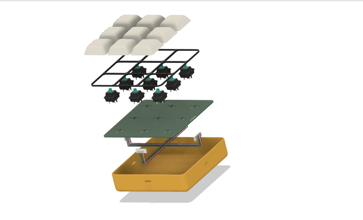
The parts of this module consists of :
The body:The main body will house the entire electronics part. There will be a main PCB that will have the
microcontroller and the switches .
The Keycaps : the buttons are inspired from the minesweeper tiles . I wanted the physical buttons match the
appearance of the digital counterpart
The keyplate: to keep the the keycaps and the PCB in place.
The electronics placement was alos integrated into the CAD models. I designed the PCB in Kicad and exported as
STEP file ,which was then imported into Fusion360. By doing this step it helped me visualize and make the overall
dimensions of the PCBs and its relative position to the body.
Initially the housing for the connector PCB was rectangular then after many other iterations it was changed to
mounting screws as the rectagular housing may hinder the flexible pcb positions
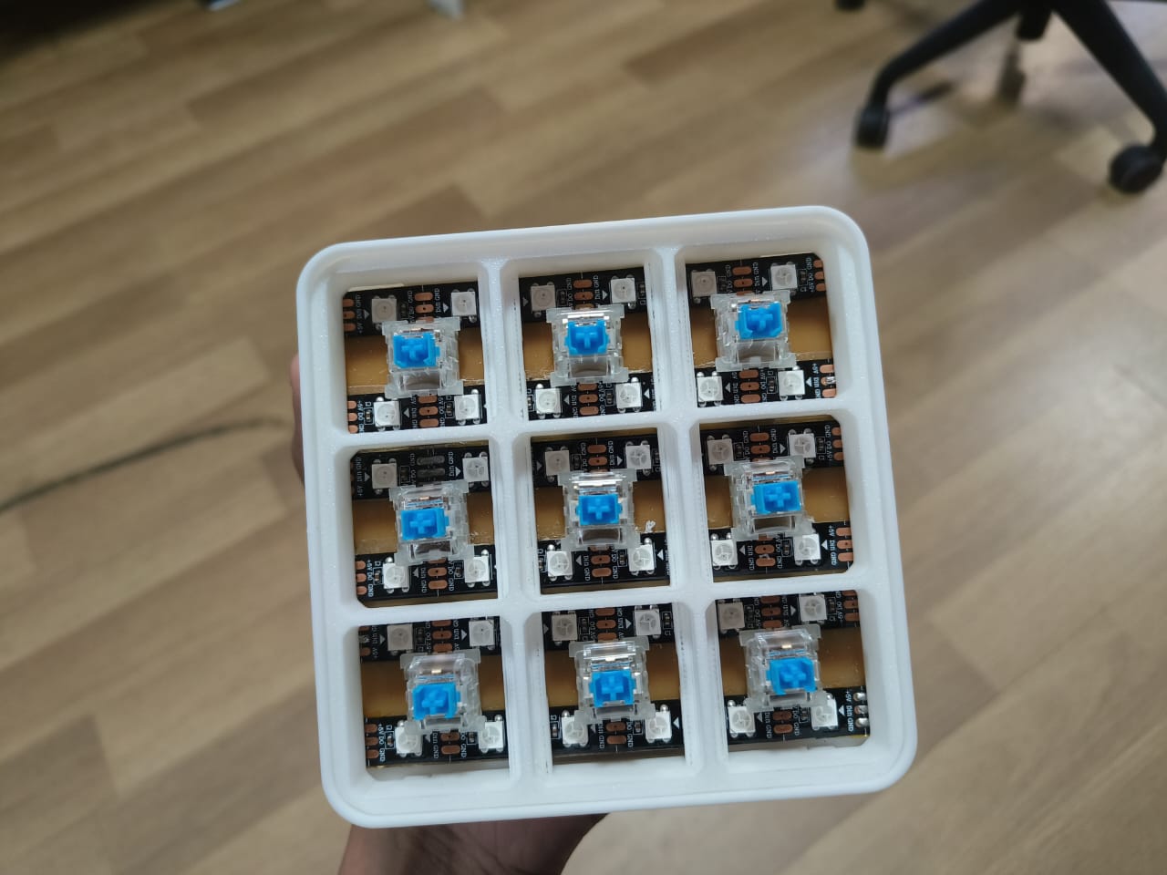
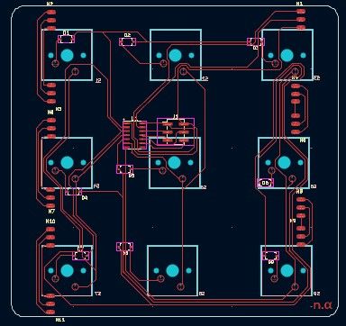
PCB Design and Production
PCB Mockup.
I started the electronics production of the project with the node module.
Components in a node module are:
ATTINY 1614
9 x Mx switches
9 x Diode
9 x Diode
Neopixel pads
2x03 Vertical Pinheader
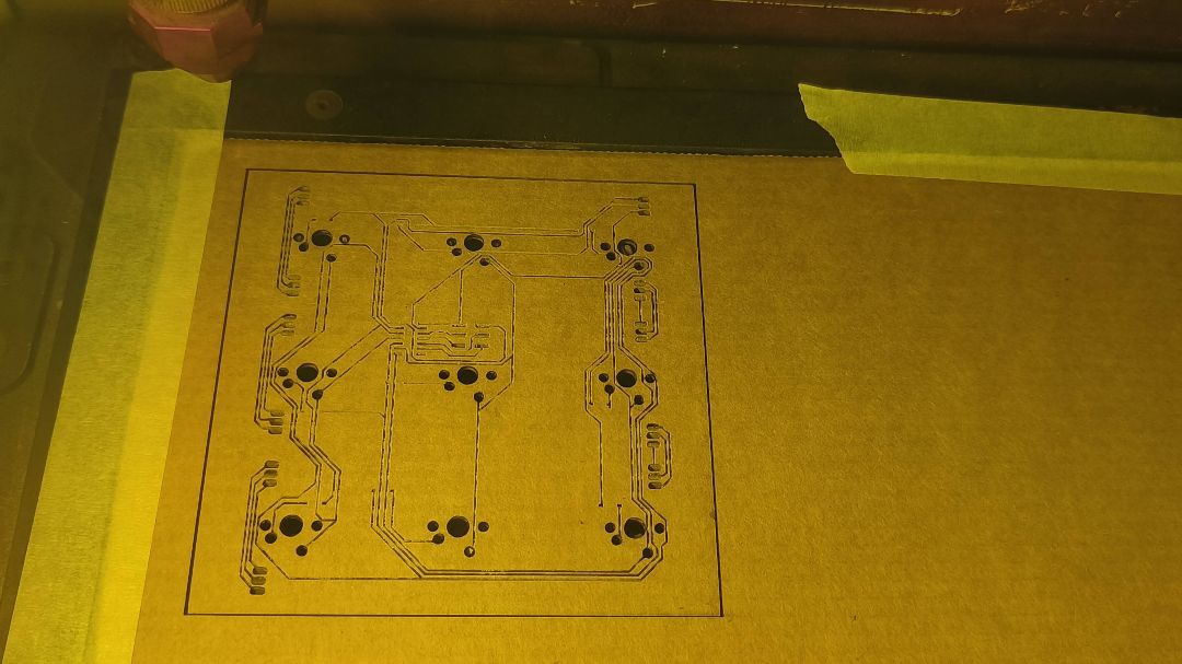
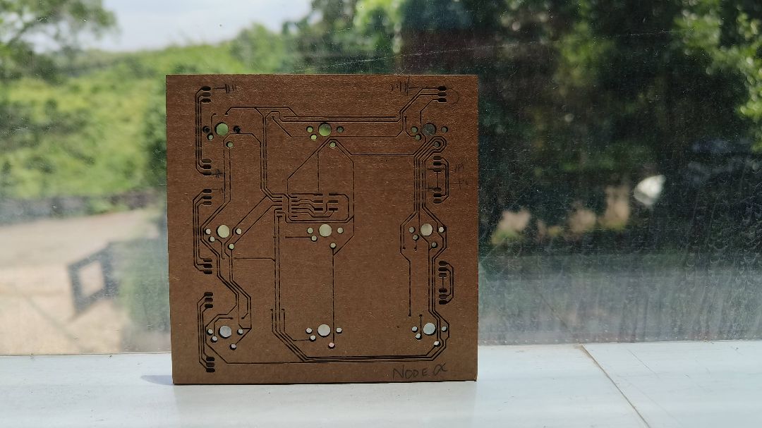
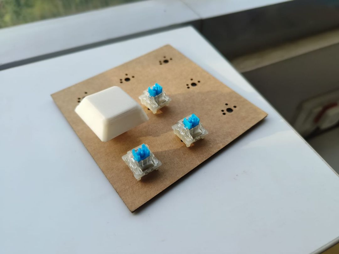
I had some doubts regarding the placement of the neopixel pads as they had to be wrapped around the pcb and the
solder part sould sit perfectly on the pads.Since the the pcb iam making is quite large , i did not want to waste
an entire copperplate incase something goes wrong. So i thought of making a mockup of the PCB on cardboard see if
everythng aligns well
I kept the pixels in place and found some misalignments.Thet were later corrected in the kicad editor.
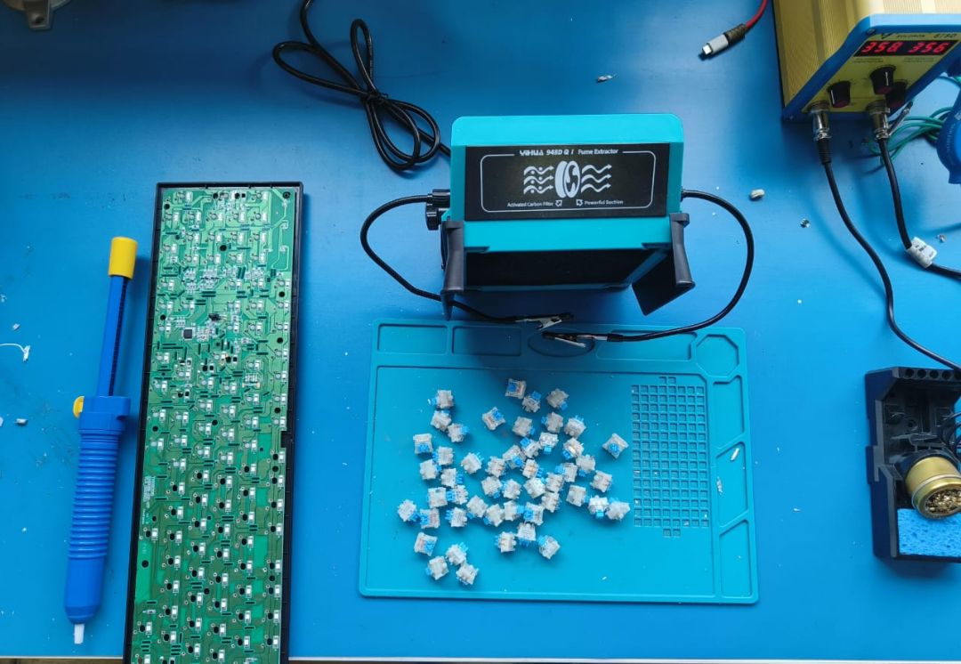
Keyboard Disassembly
As I required a lot of switches for my project , it seemed more feesible to buy a mechanical keyboard and take out
the keys rather than buying individual switches as that would add more to the cost. After making the purchase I
realised that the switches were not swappable , whih meant that each of the switches had to desoldered according to
my requirement.
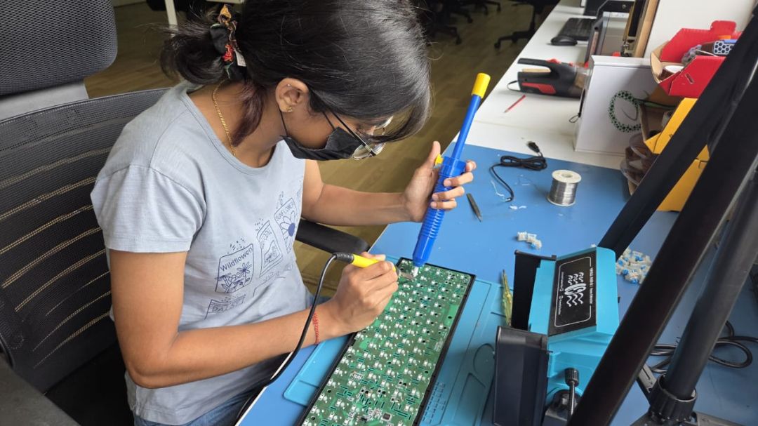
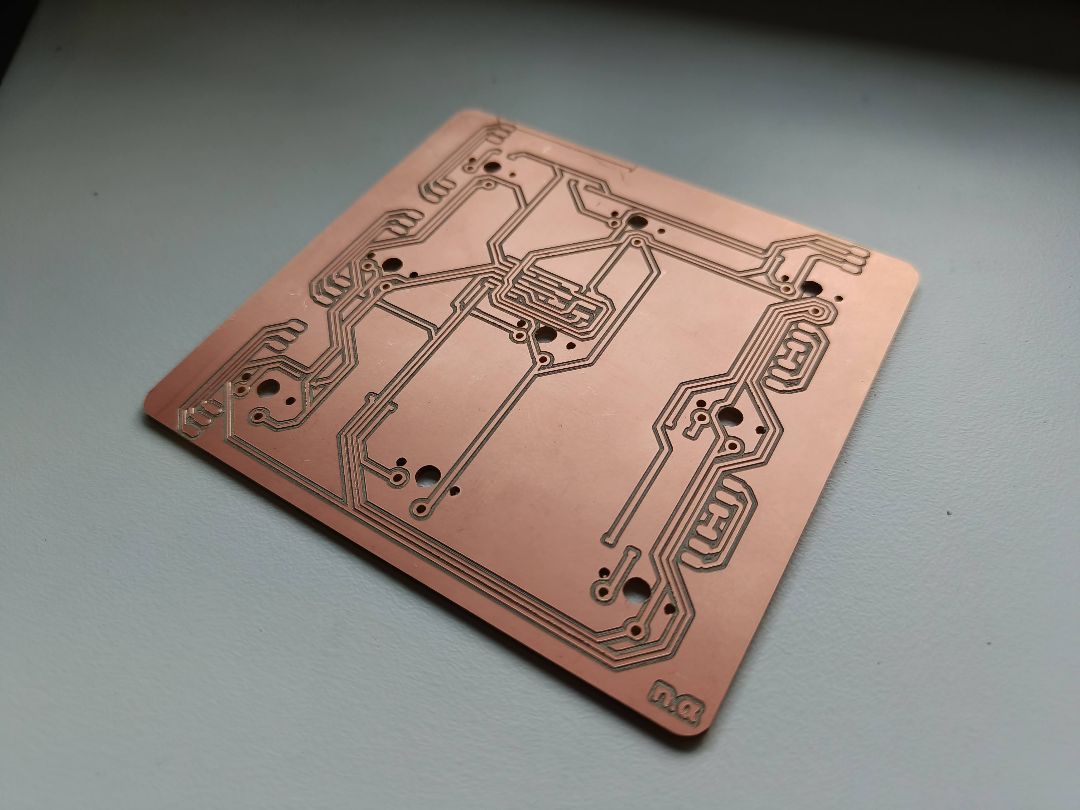
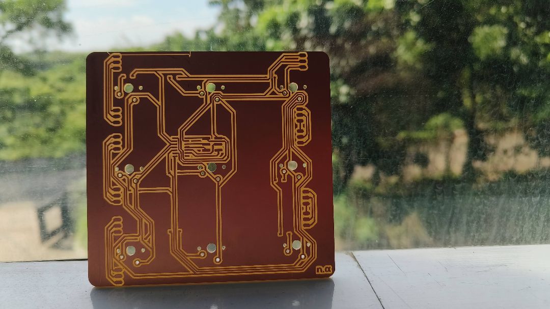
PCB production
I milled out the PCB and moved on to the pick and place machine to place the parts.
After milling out the PCB and placing the components , while trying to measure the length of the led strip to be
cut, i realised that the switches and the LEDs did not match . There was a misalignment of one row of switches
that affects the whole placement.
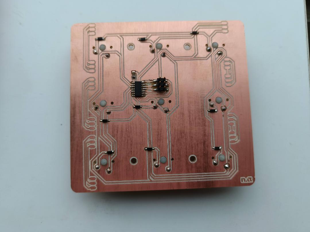
So i had to go back into the kicad editor and then realign all the switches . This time to make sure the
measurements were correct I edited the snap to grid number to the measurement i required from the centre of one
switch to another.
The pad position were corrected as well. I had forgotten to add a capacitor in the previous circuit so i could
add that here now.
The PCB was filled out again and the neopixel
Strip length was checked. After confirming everything was alright i moved on to solder the components on to the
PCB.
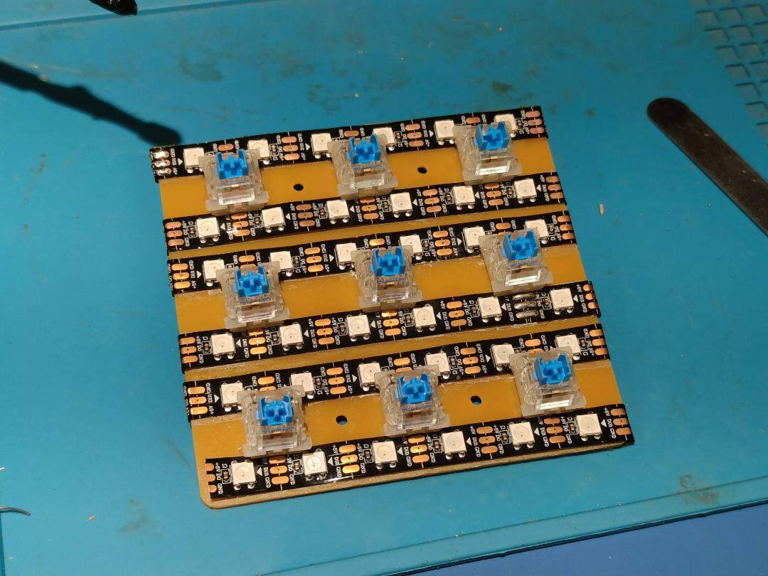
Next the led strips had to be fixed . I first cut the strip to the length of the pad. One led would have to be
removed because it won't be visible as it will be on the flip side of the board.
Then I stuck kepton tape on the edges of the traces to avoid any interaction between the copper cladding and the
wires within the strip.
I stuck double sided tape on the outer edges of the switches and stuck the strip on to it. Then I soldered the
strip to the PCB.
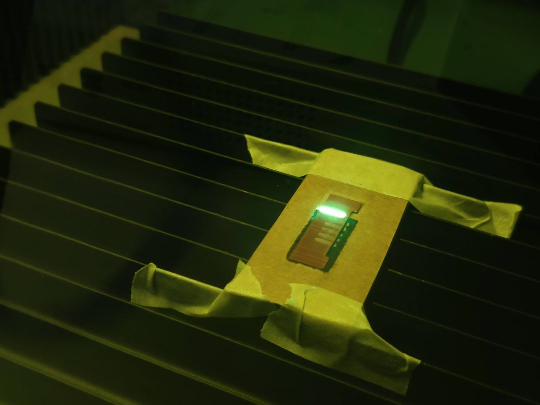
This was repeated for all the rows.
A connection had to be established between the din dout pads of the led that were removed. A copper wire was
soldered to make this connection.
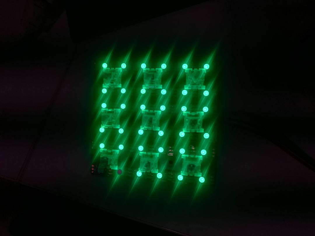
After the soldering, i tried to program the PCB to check if everything was working correctly. I uploaded the
buttoncycler example code to do a colour change when a switch was pressed. Everything looked good so far:)
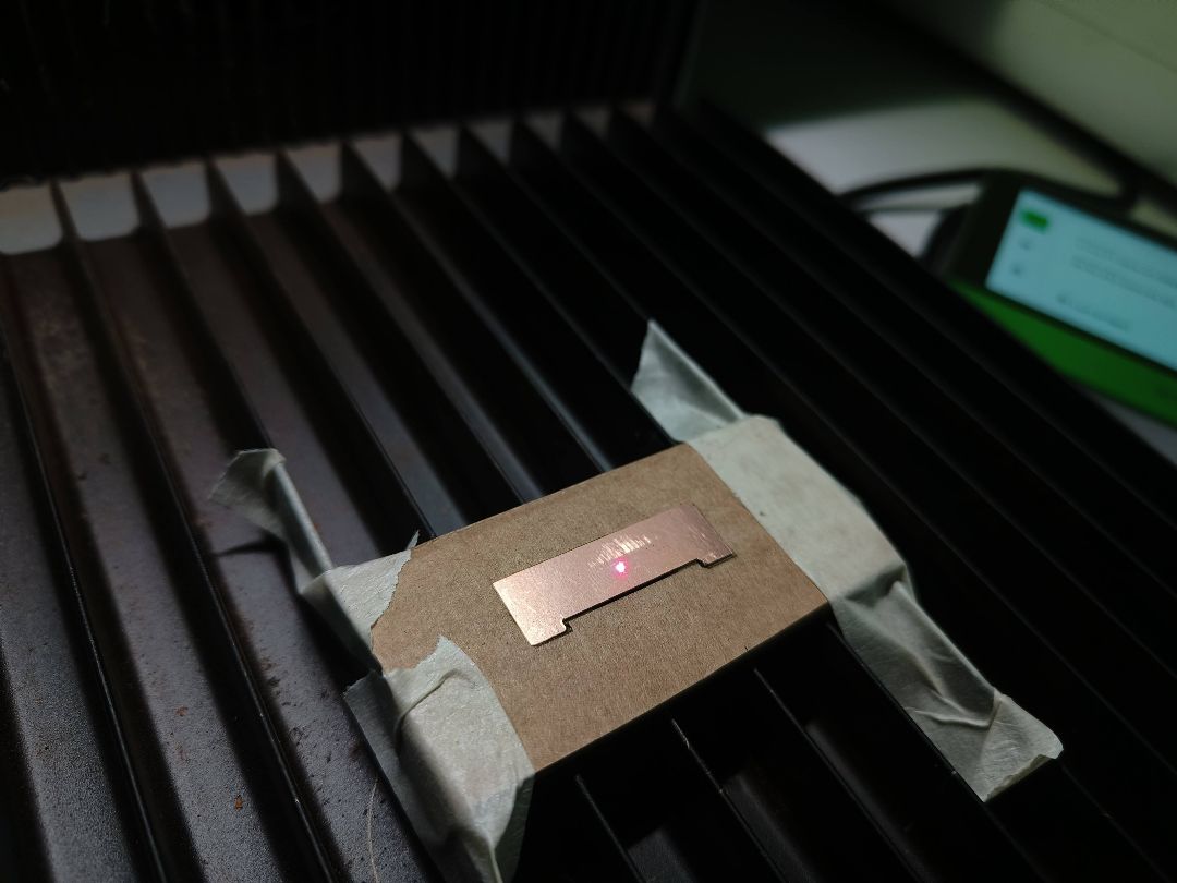
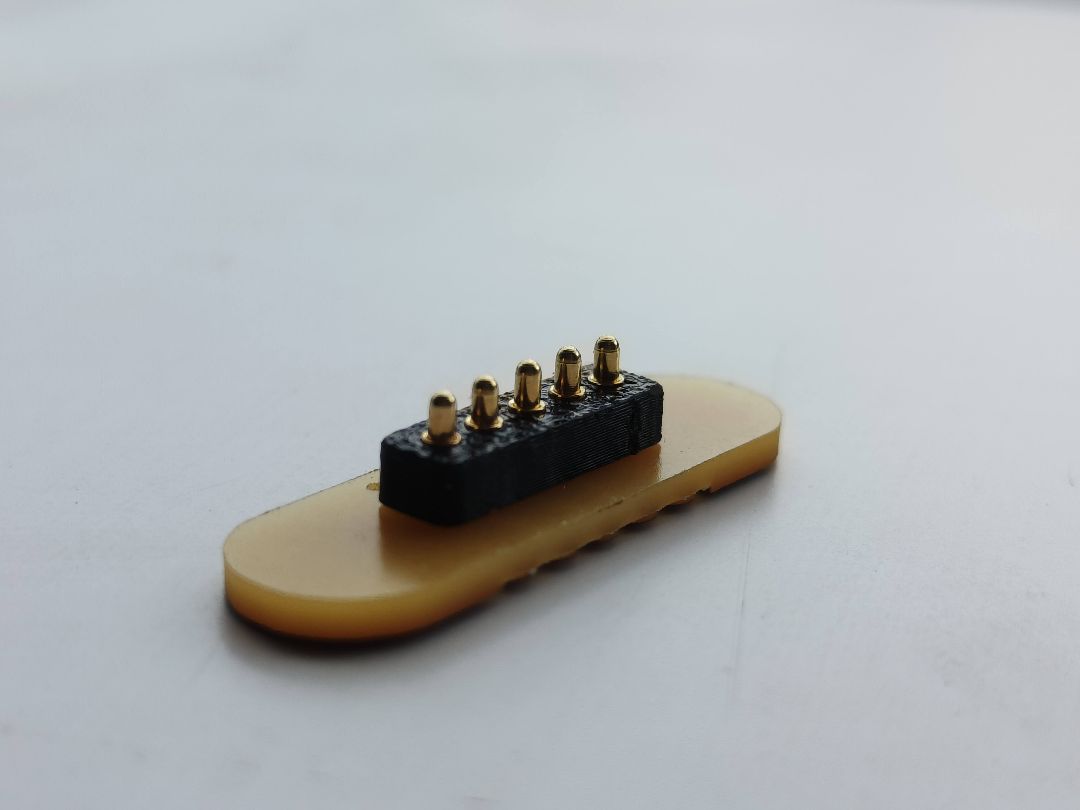
Making Pogo connectors.
I had to think of ways to make the pogo connectors as they are quite expensive and to buy as many as i required may
not be feasible within the scope of this project.
I referred to some videos to make the connectors and went through some design iterations . I made a few mock pieces
to test if it would work properly.
Mockup 1
The first idea was to make a PCB tht would have pin header connection from the top of the keypad PCB , on which
the Pogo connectors mounted on another smaller PCB will be attached perpendicular it.
First to test the concept i tried making a small scale mockup to check the attachments. Two PCBs were made with
just the pads for the connections and the slot for attaching them.
There were some issues faced while milling the PCB due to its small size and since the PCB is double sided. When
the PCB had to be flipped for tracing and cutting the other side , it would fly off because it wouldn't stick
properly. I spent some time trying to make the cut ,so i thought of other ways the PCB could be produced
efficiently. My instructor suggested to use the milling machine to just cut the PCB and then take it to xtool to
engrave it. To keep the PCB in place a cardboard jig had to be made. Even this method did not seem as effective as
it looked on paper. The fit was was checked for the two PCBs and some adjustments had to be made
Also while making the CAD model for the module , it was noted that the size required for the PCB would be
quite large for a double sided PCB (our lab has a limitation on the size for double sided pcbs). So we went back
to
the board to test another method.
Mockup 2
This was initially the plan we were supposed to go ahead with ,but after some thinking and updations we made a
few alterations to it.
Basically the idea is to make the small PCBs to attach the pogo pins and the take connections from this PCB to
the PCB with the connection from the keypad PCB via wires. Tecnically its the same concept as before but we can
make the central PCB smaller and save space.
While making the CAD model i realised a housing had to be given for the pogo pins. The CAD model has to be
altered to make space for the housing too.So that was also done parallel to this process.
For this mockup I just had to make the small PCBs and make sure it fits with it mock 3d prints made. I had made
a careless mistake on the 3d model where the housing had to sit, even though I made it correctly on CAD i exported
the wrong version.
After reprinting the case the PCB with housing was tested and it was fitting perfectly.
Once the fit was checked I moved on to solder the pins on to the PCB along with the housing.
The fit was checked again and I also kept another PCB to act as the landing pad for the pins
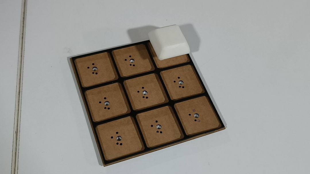
Mockups and Testing
Since printing an entire body then checking whether any corrections were required would be time consuming as
well as waste of resource if the end product of the prints were rendered unusable. So i was instructed to print
each of the parts that required testing separately in small portions so that it becomes easier to correct the
mistakes and save material and time.
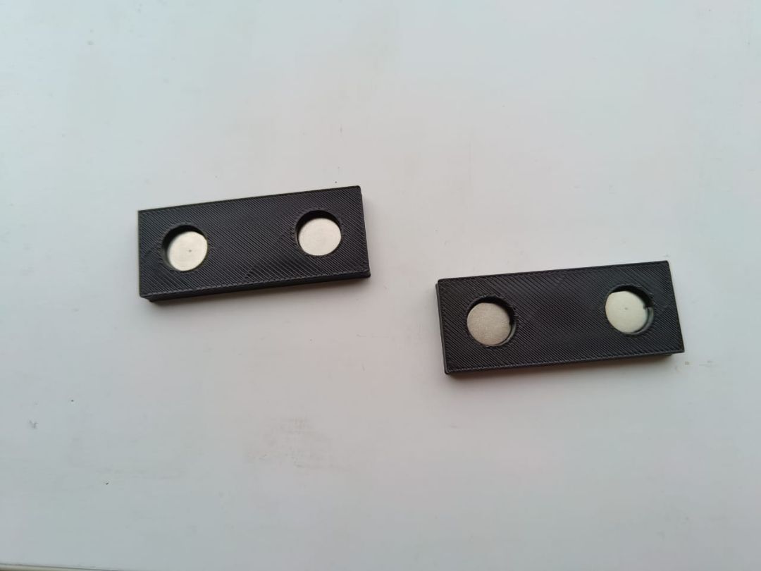
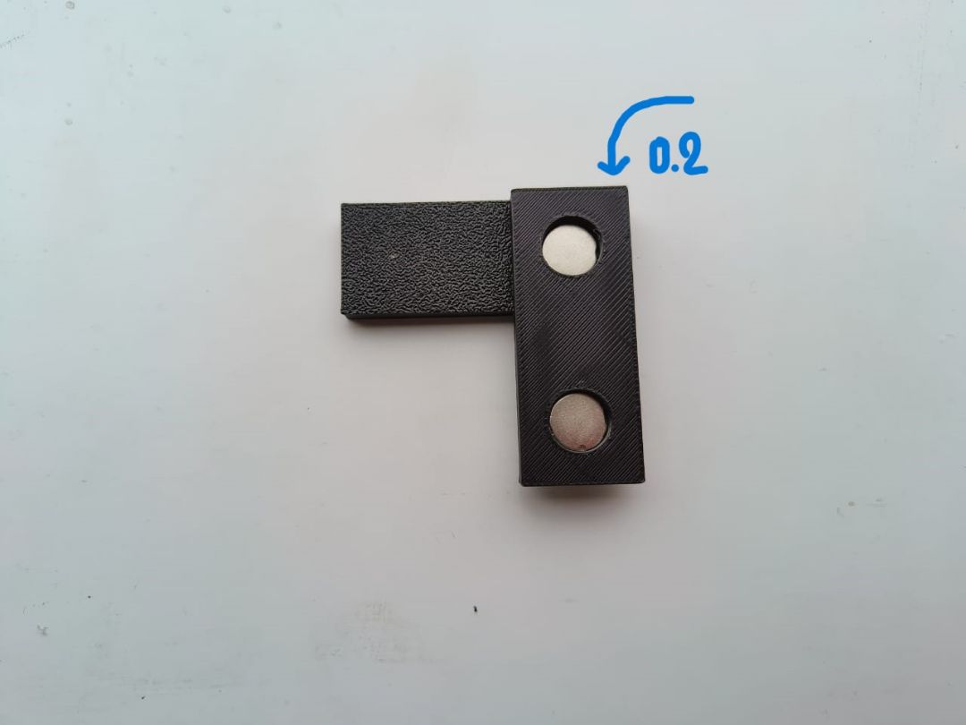
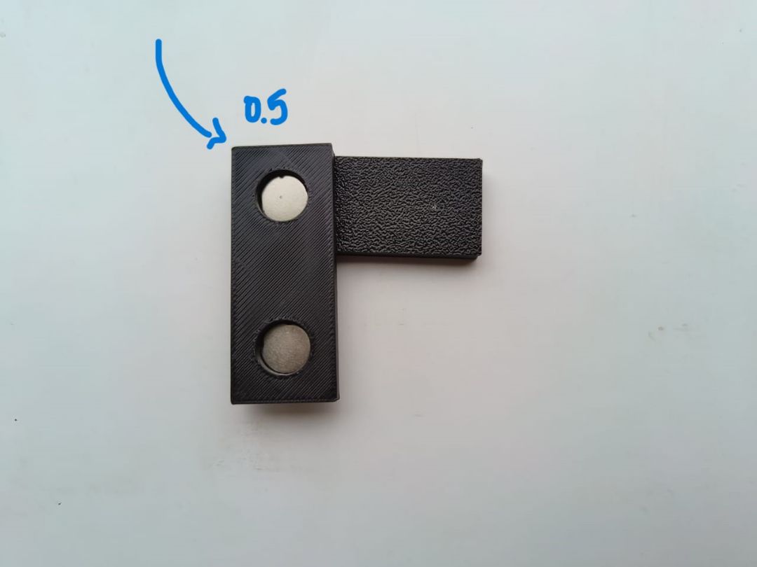
Checking magnetism
I checked the wall minimum wall thickness required for the nodes to stick to each other
2 prints were made with 2 slots where one was of 0.2mm thickness and another with 0.5mm thickness to test.
I felt that the 0.2mm thick wall was required for the modules to stick firmly.
Locking for the Pogo connector PCB slot
A locking mechanism had to n=be made to keep the PCBs in place so that when a module is connected it doest push
out the PCB from its slot.
Parts of the body was made to test out how the overall connections would work.
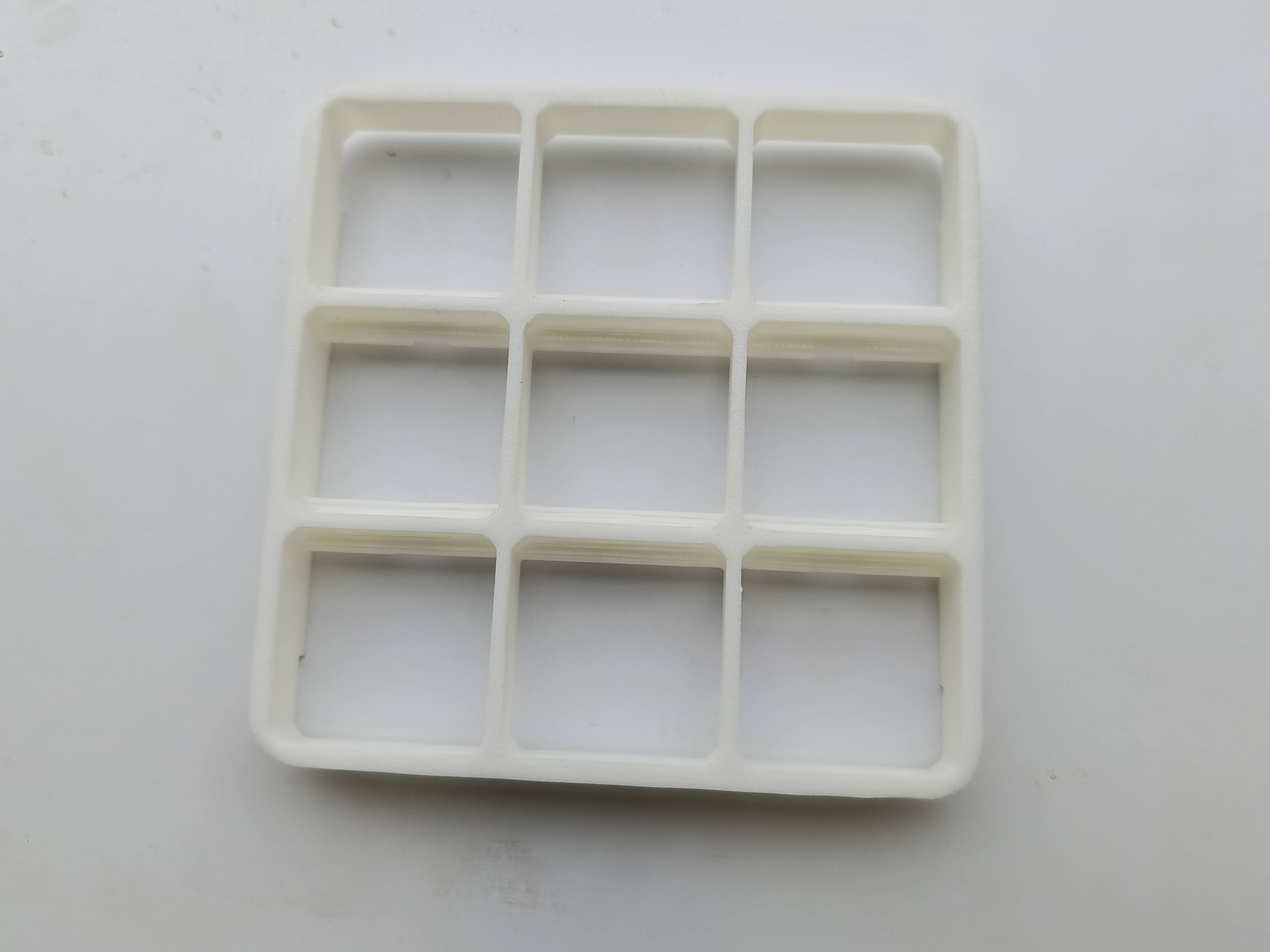
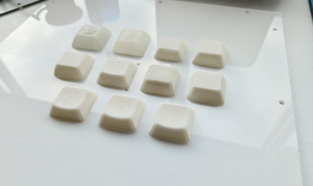
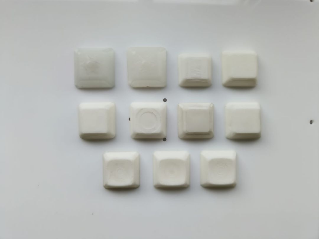
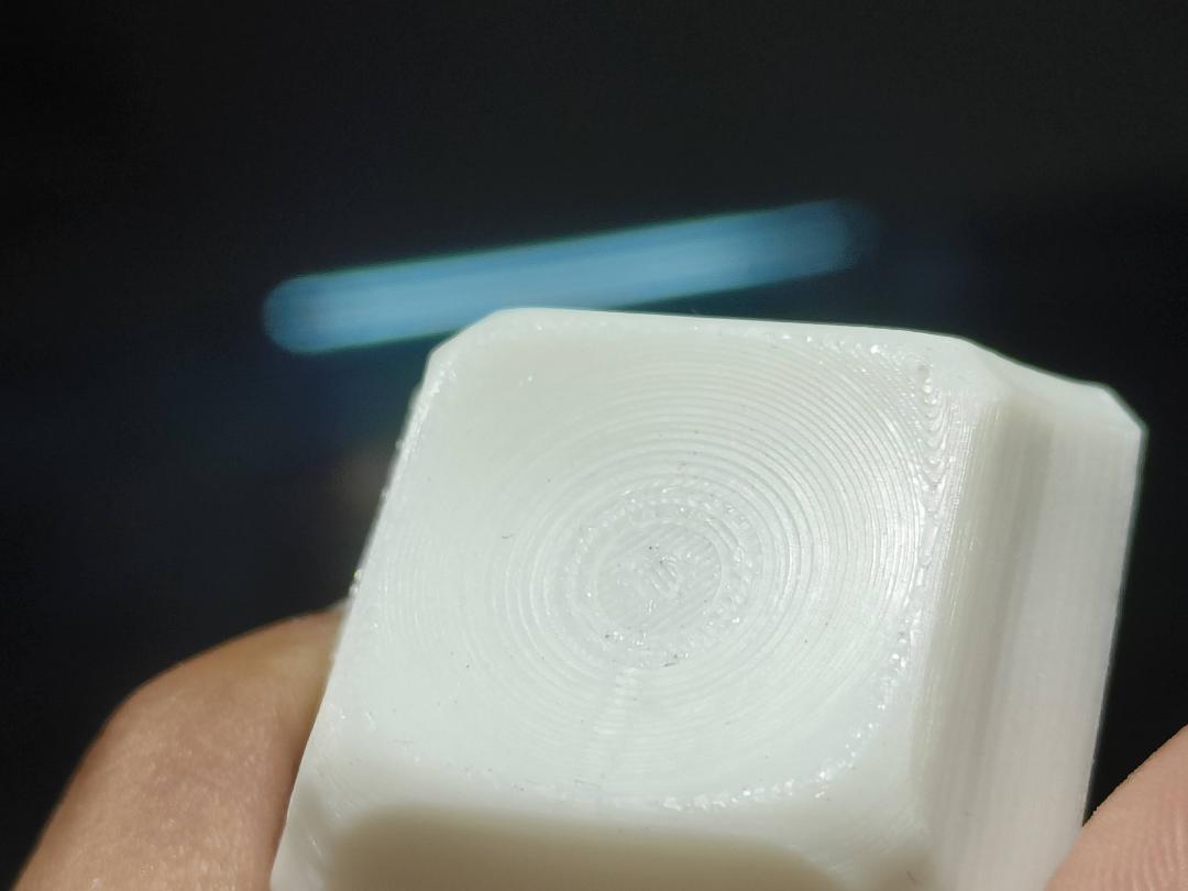
Keycap Iterations
I used the similar method for casting the buttons as i did during the molding and casting week. The only
difference being that the mold was directly 3d printed as a button and the silicon was cast over it.
To decide which was the best keycap for my product , the keycaps went through multiple iterations, changing the
dimensions, the dip on the top and size of the stem, to reach the final design of the keycap. Each design was
fisrt modelled in Fusion360
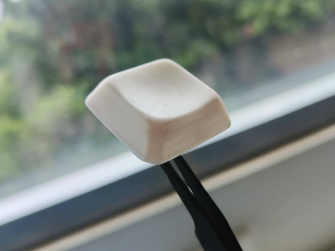
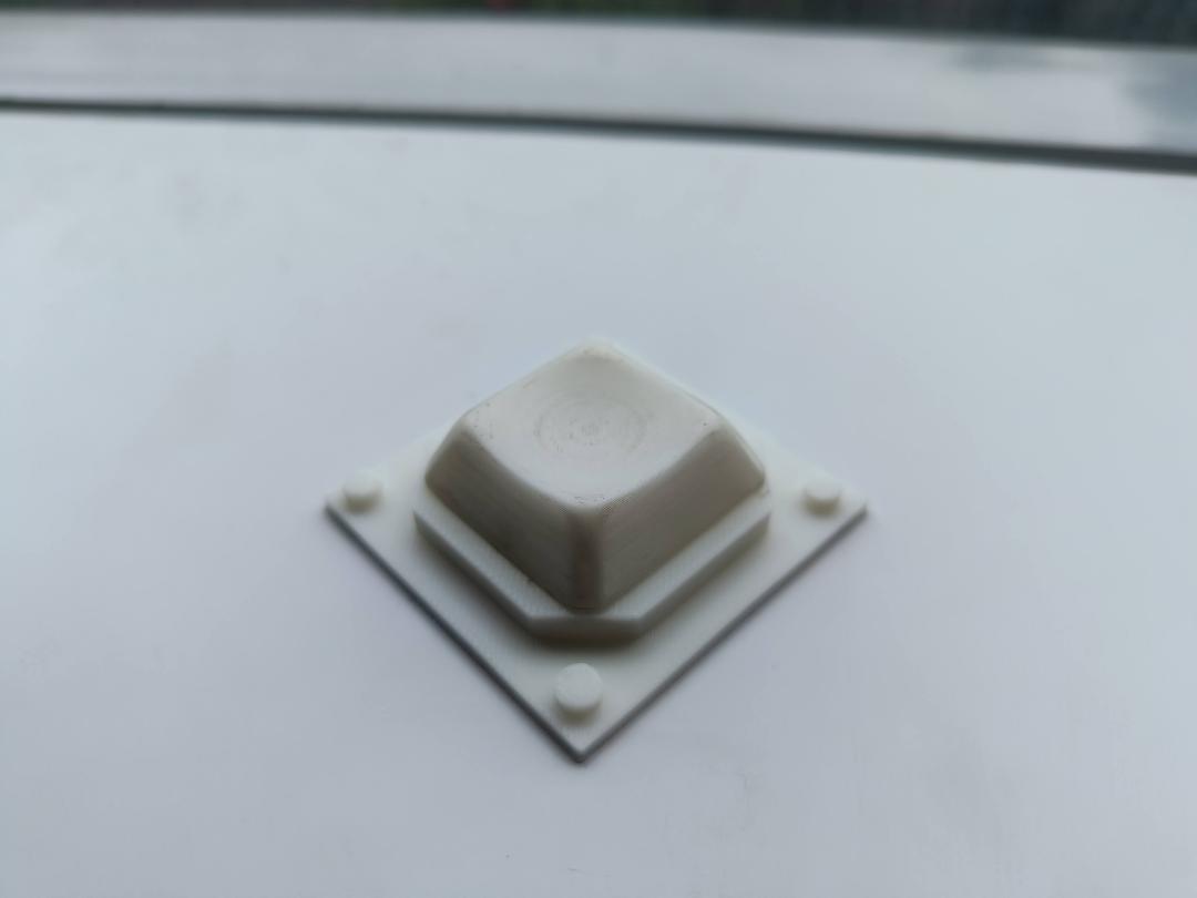
Molding and casting the Keycaps
I 3d printed the final design and smoothened the layers lines by sanding it
throughly with 320,220 and 100 grades of sandpaper.
I had to make an adapter to place the keycap on a surface so that the top surfcae can be poured with silicon
rubber carefully with the keycap shifting its position.
I also made a mold box using acrylic. Acrylic was laser cut and fixed using finger joints. The adapter with the
keycap will fit within this box and silicon will be poured.
It is then casted with epoxy resin. The finish and colour cme out pretty good. The resin did not reach
every surface so i am trying to achieve a proper finish now.
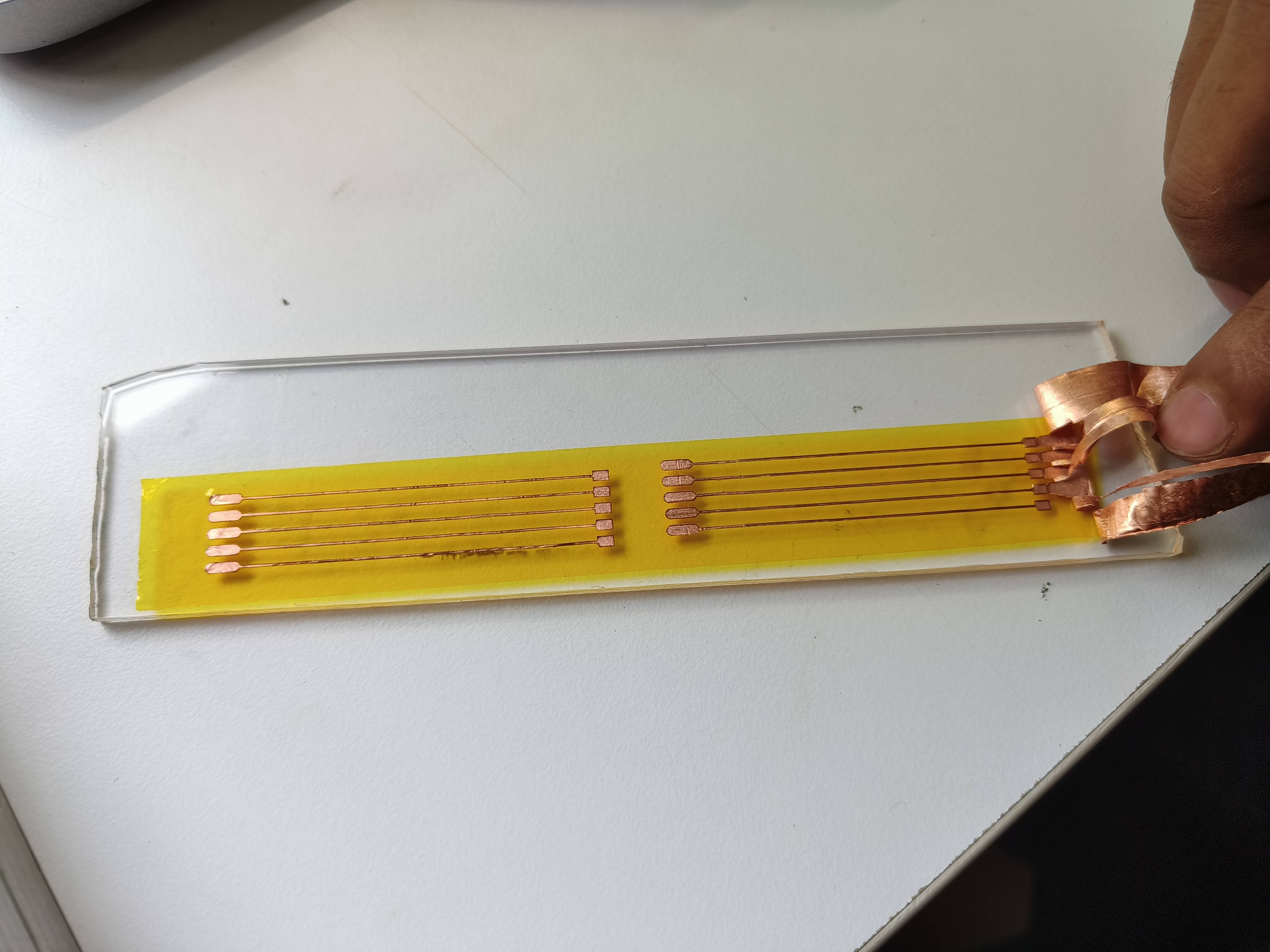
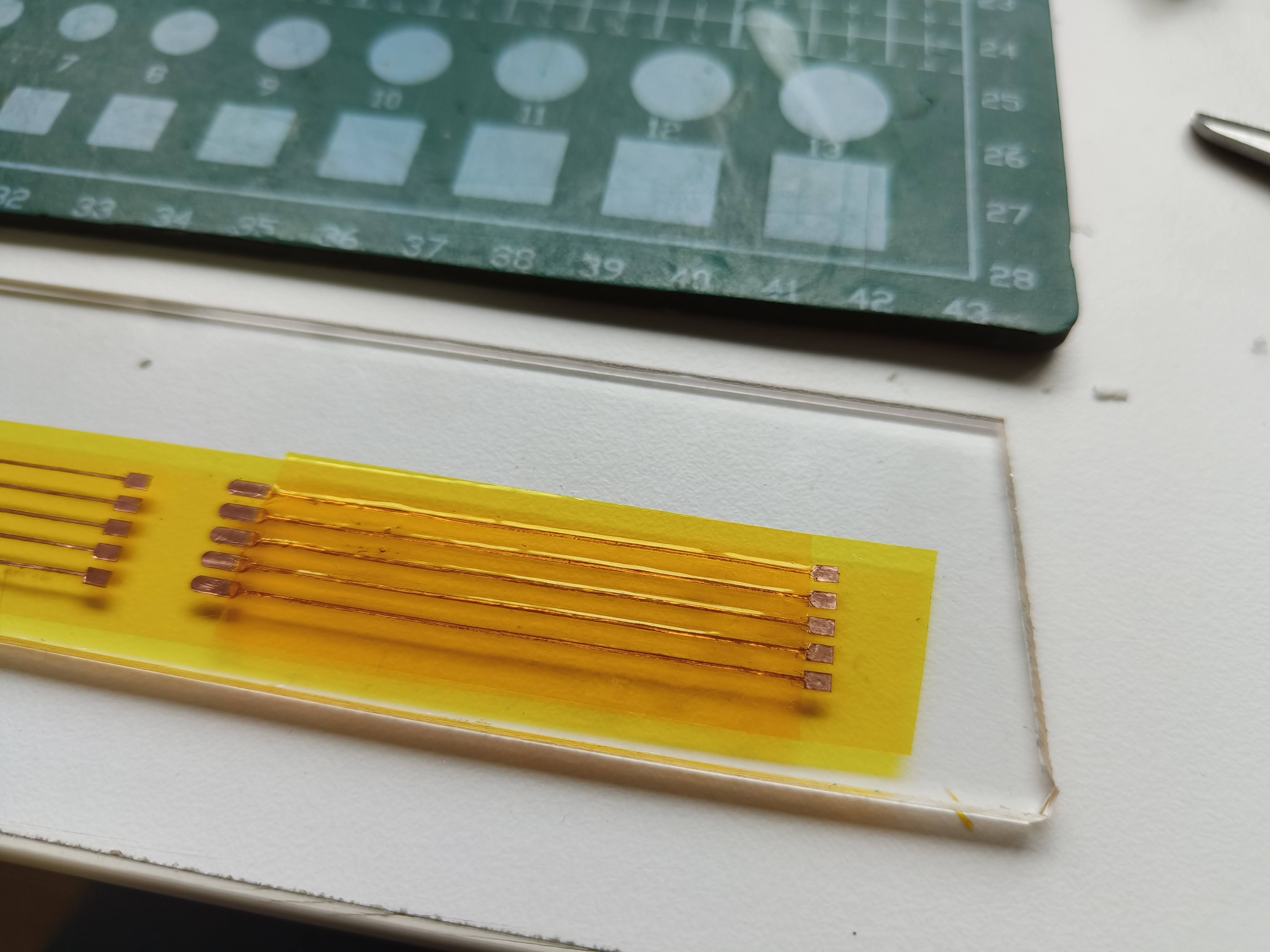
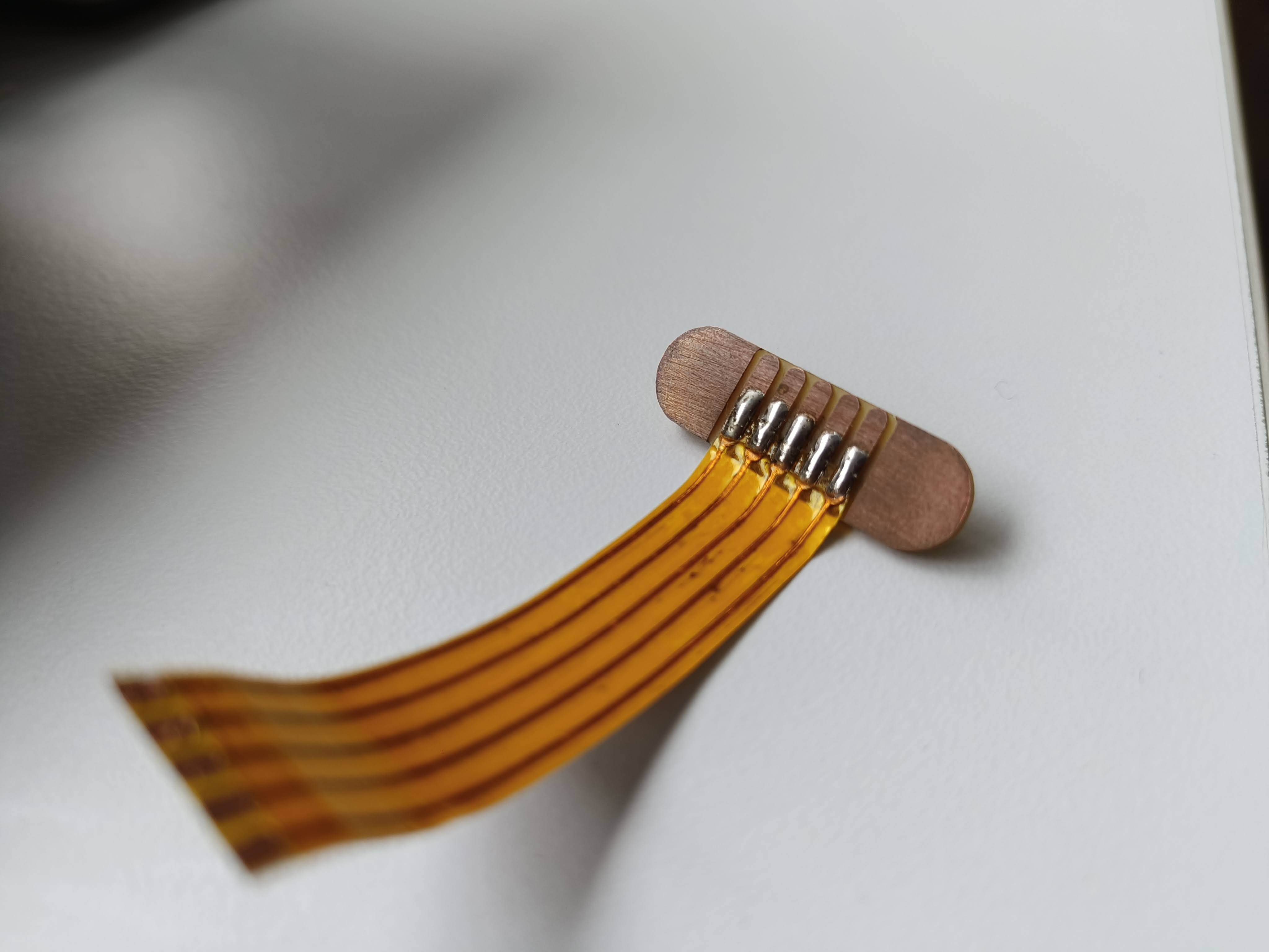
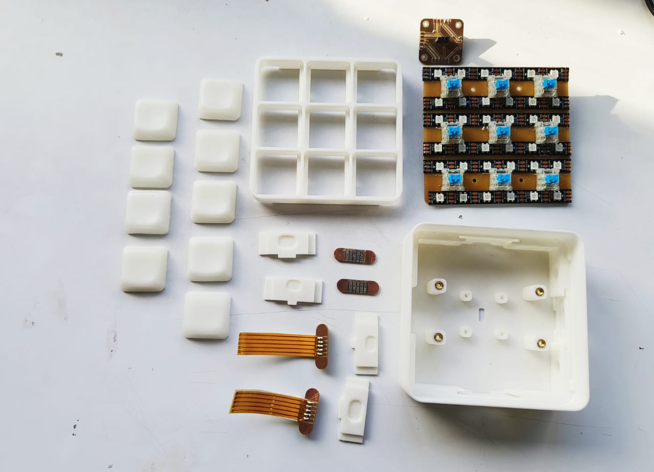
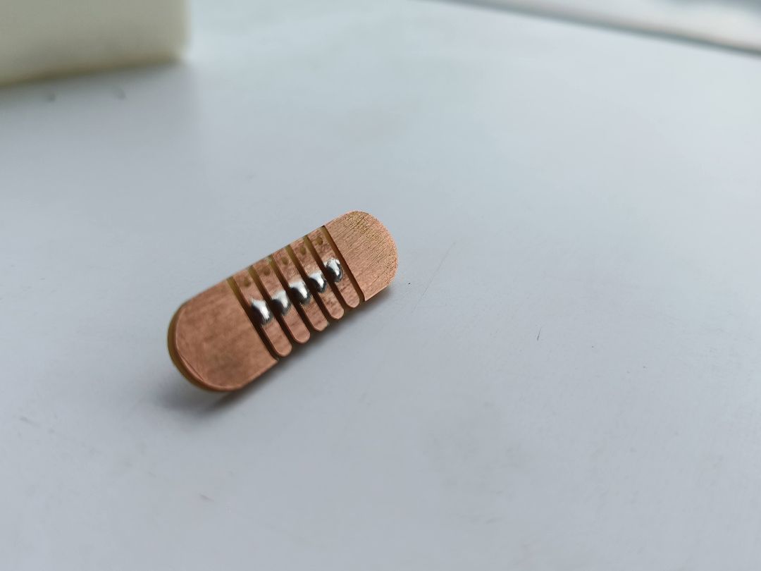
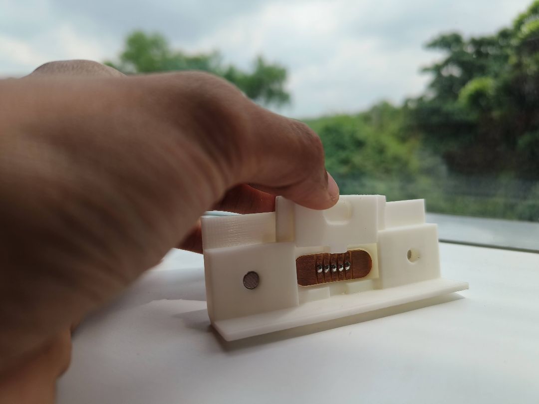
Flexible PCBs
To establish the connection between the pogo pins and the connector bottom PCB I made flexible circuit. I wanted the
housing to be neat and not tangled up with wires going everywhere.
Saheen gave this idea to make use of copper tape and kepton tape to make the traces . It is similar to the flexibile
PCBs that is sending mobile phones.
To make them these :
First a piece of Kapton tape was stuck on clear acrylic. On top of this a copper tape was stuck in place.
Then using the traces I made in Kicad after measuring the length between the PCBs , it was laser cut using
Xtool f1 ultra. The reason we stuck the strip on transparent acrylic was that the fiber IR laser won't cut
through the material.
Hence we will be able to peel the residual copper from cutting the traces from the surface easily.
Another Kapton tape was stuck on top of the the copper traces so that the copper part gets sandwiched between
the
layers of Kapton tape.
This sandwich of tapes was then peeled from the acrylic and then stuck on some backing paper
to be used later when everything will be assembled.
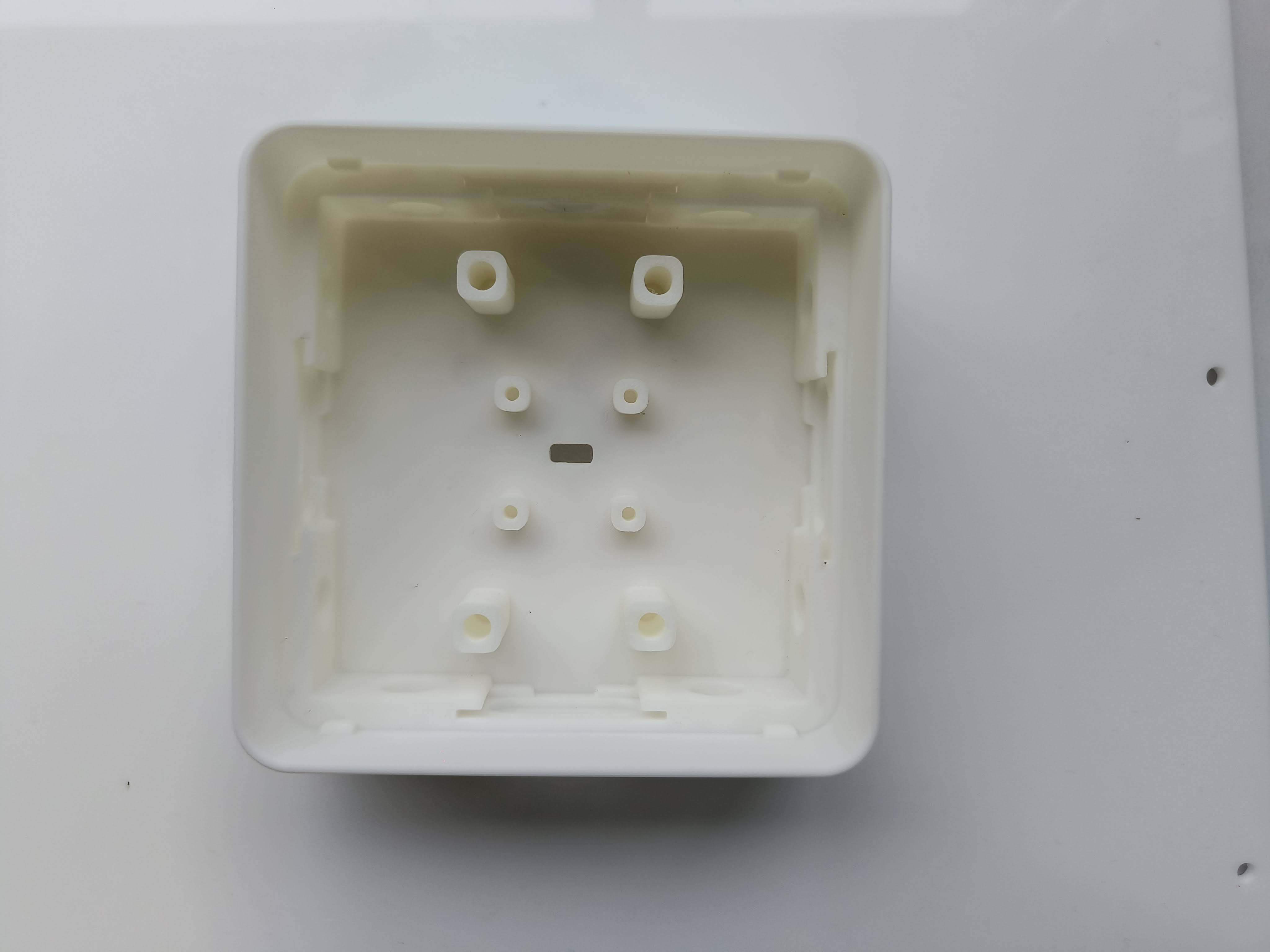
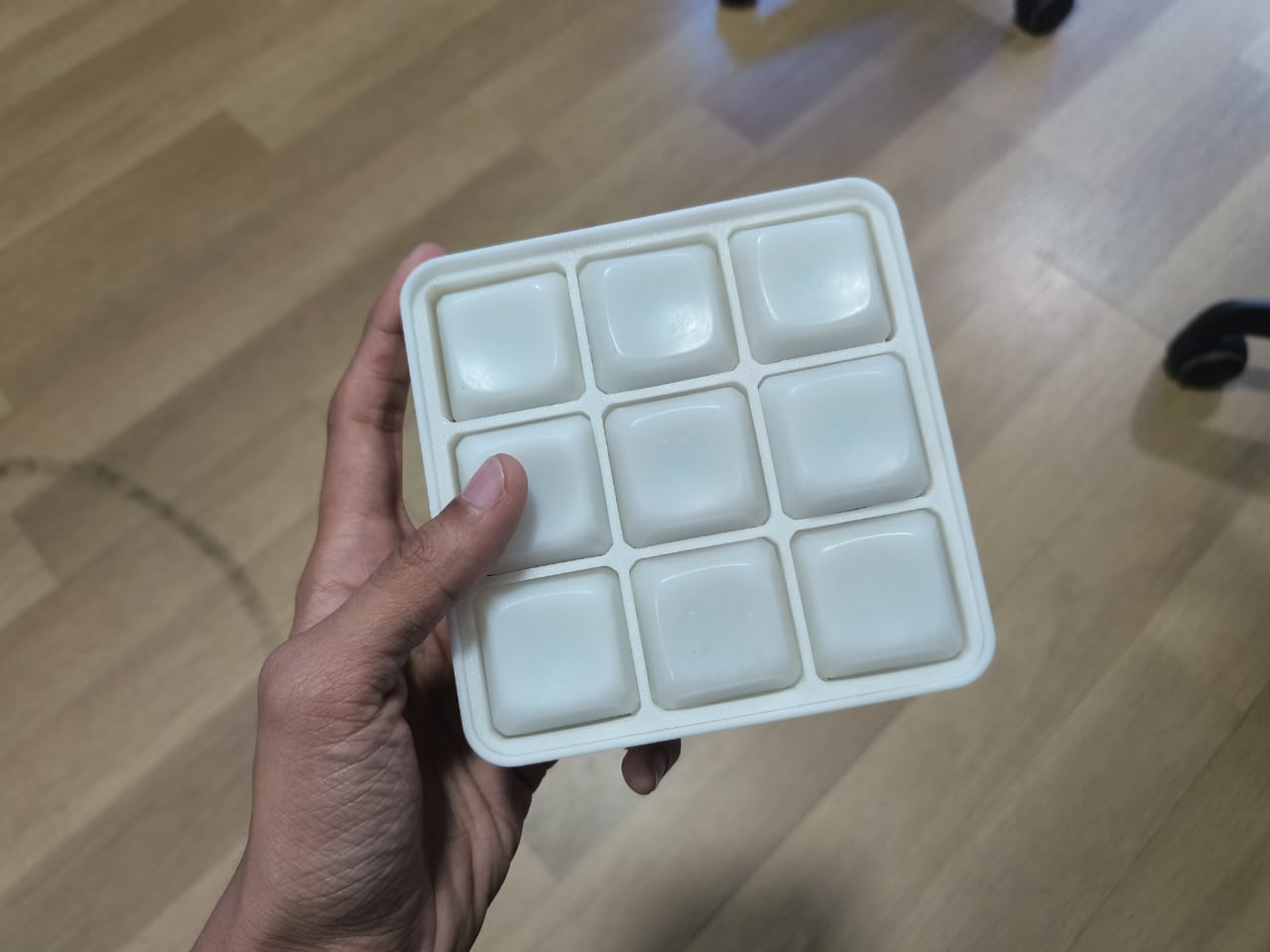
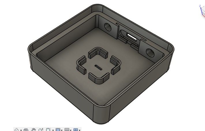
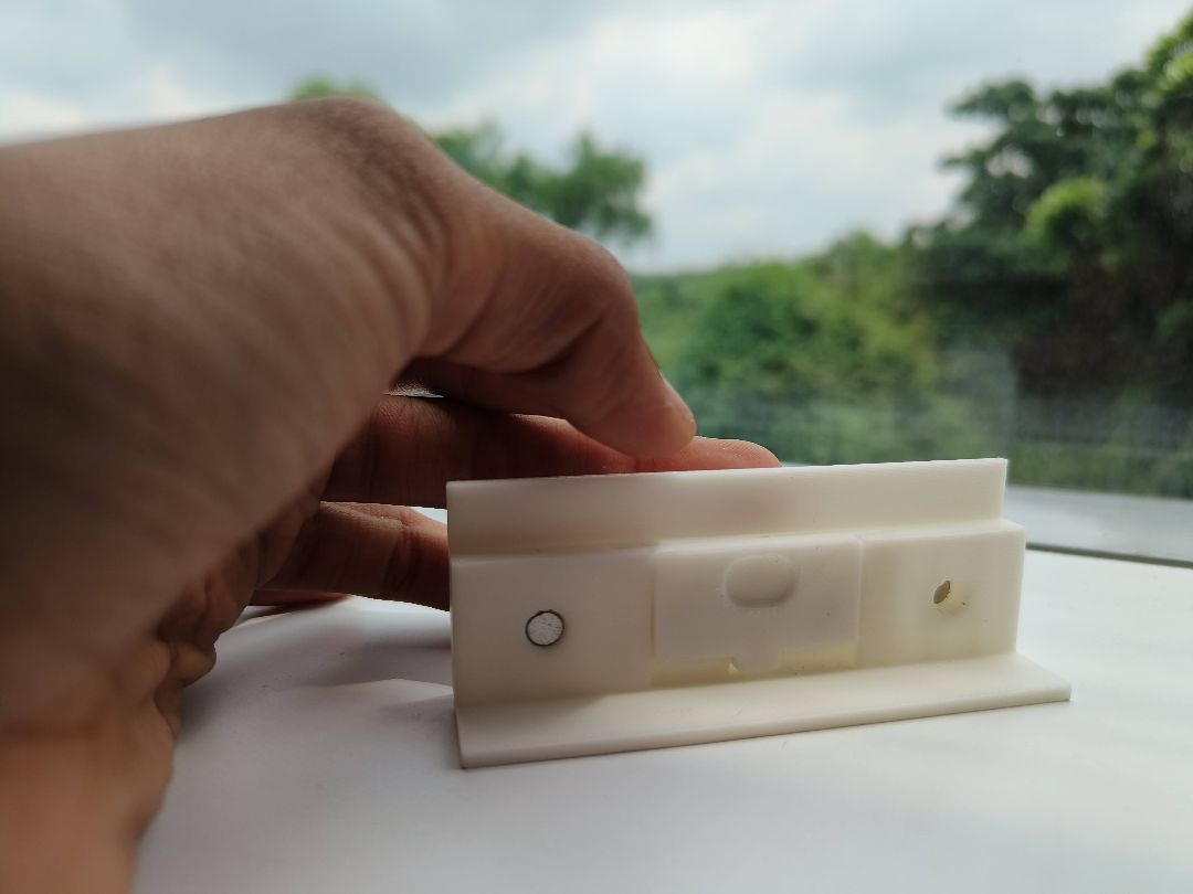
Body for module
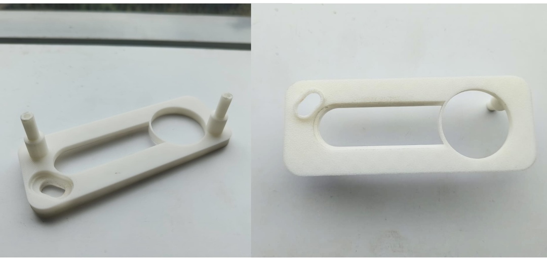
After all the testing for the parts of the body was done i printed the entire body and keyplate .
All the parts of the body was assembled. There was a mismatch in dimensioning of the PCB to the body as i did
not take into account the thickness of the neopixel strips. So i had to print the body again and this time
everything came out right.
The keyplate has notches at the bottom so the the head of the mounting screws locks in with the plate .
Threaded inserts were inserted to the body for the M3 screws to fix the PCB
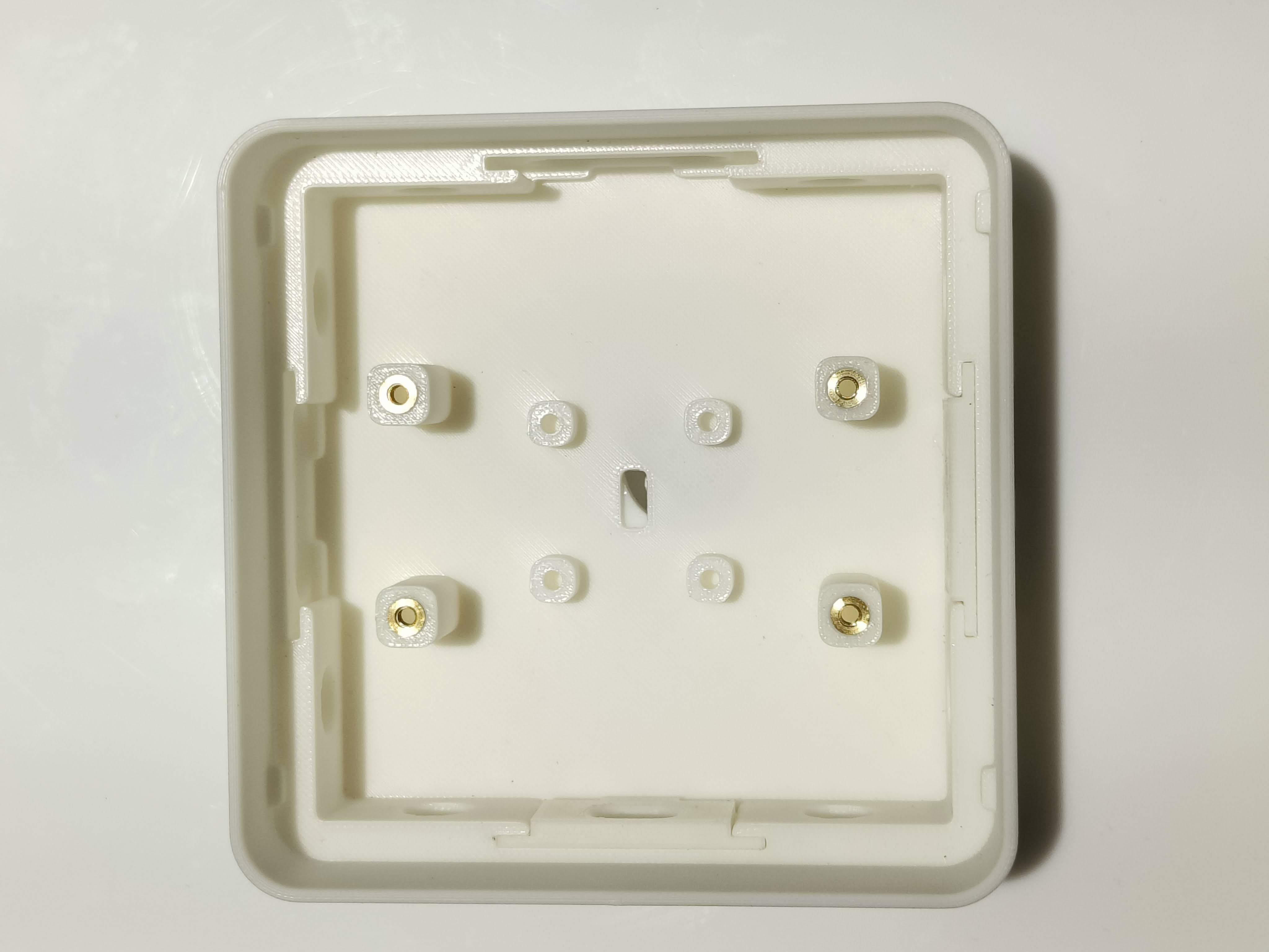
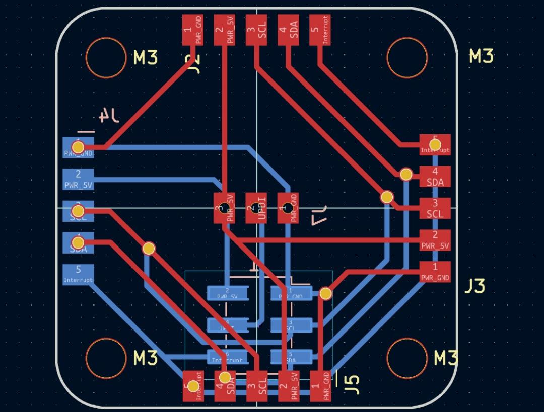
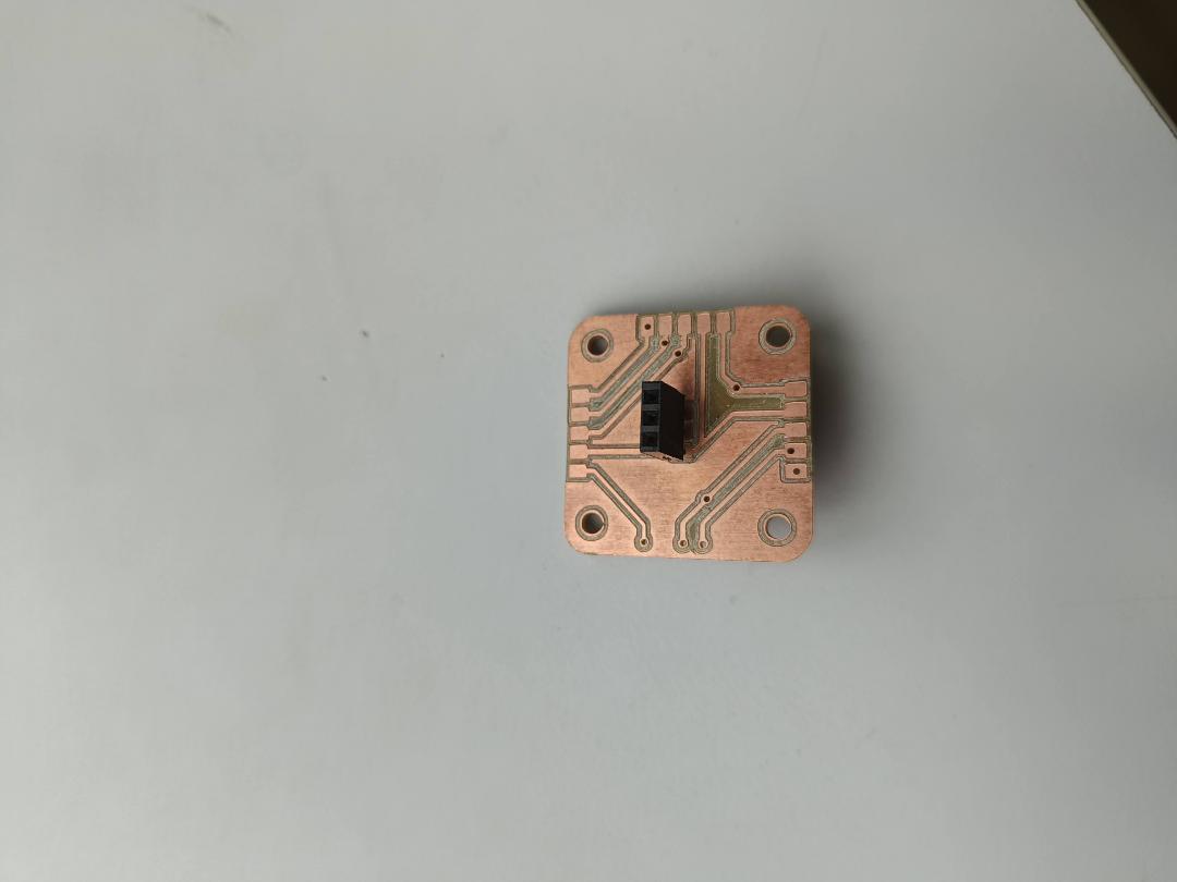
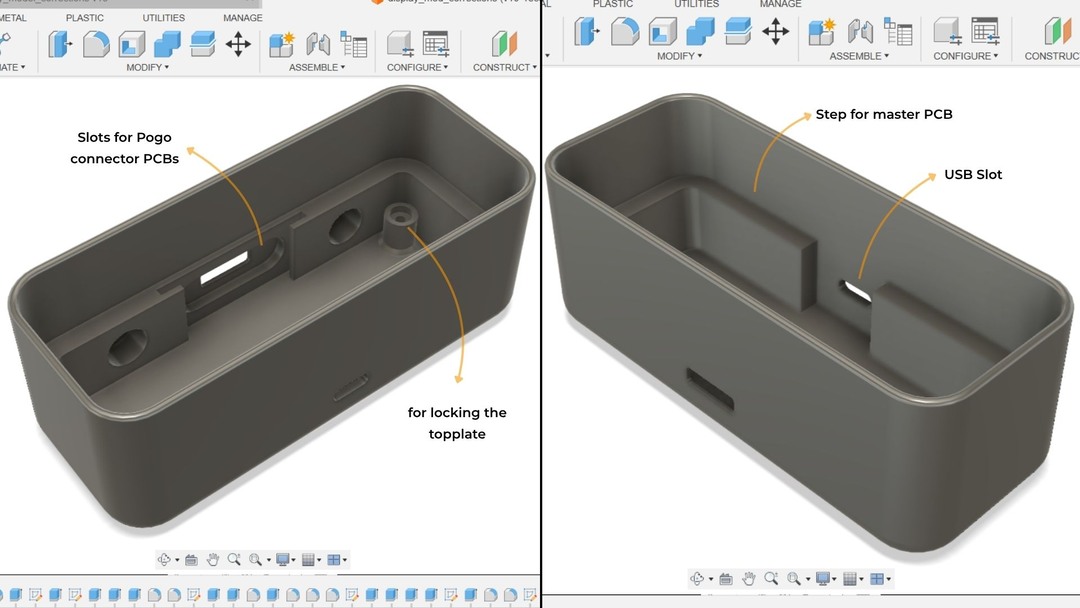
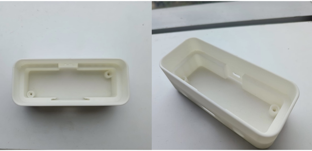
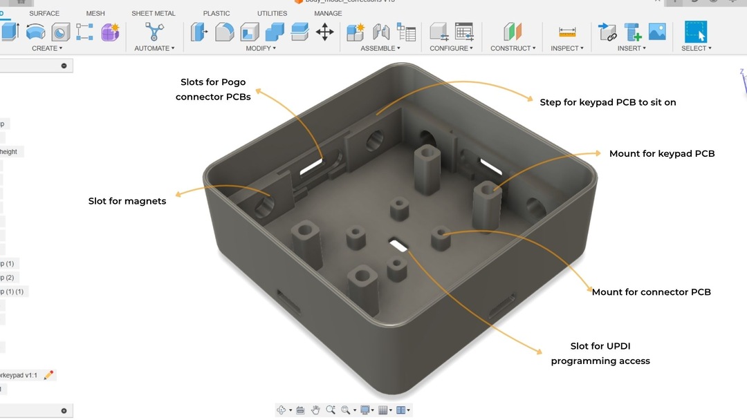
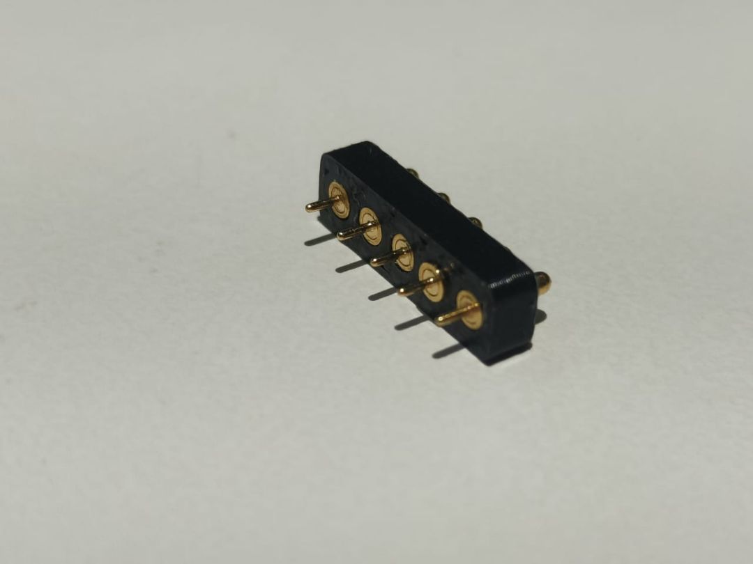
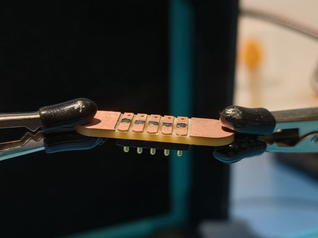
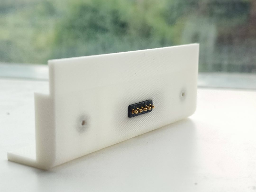
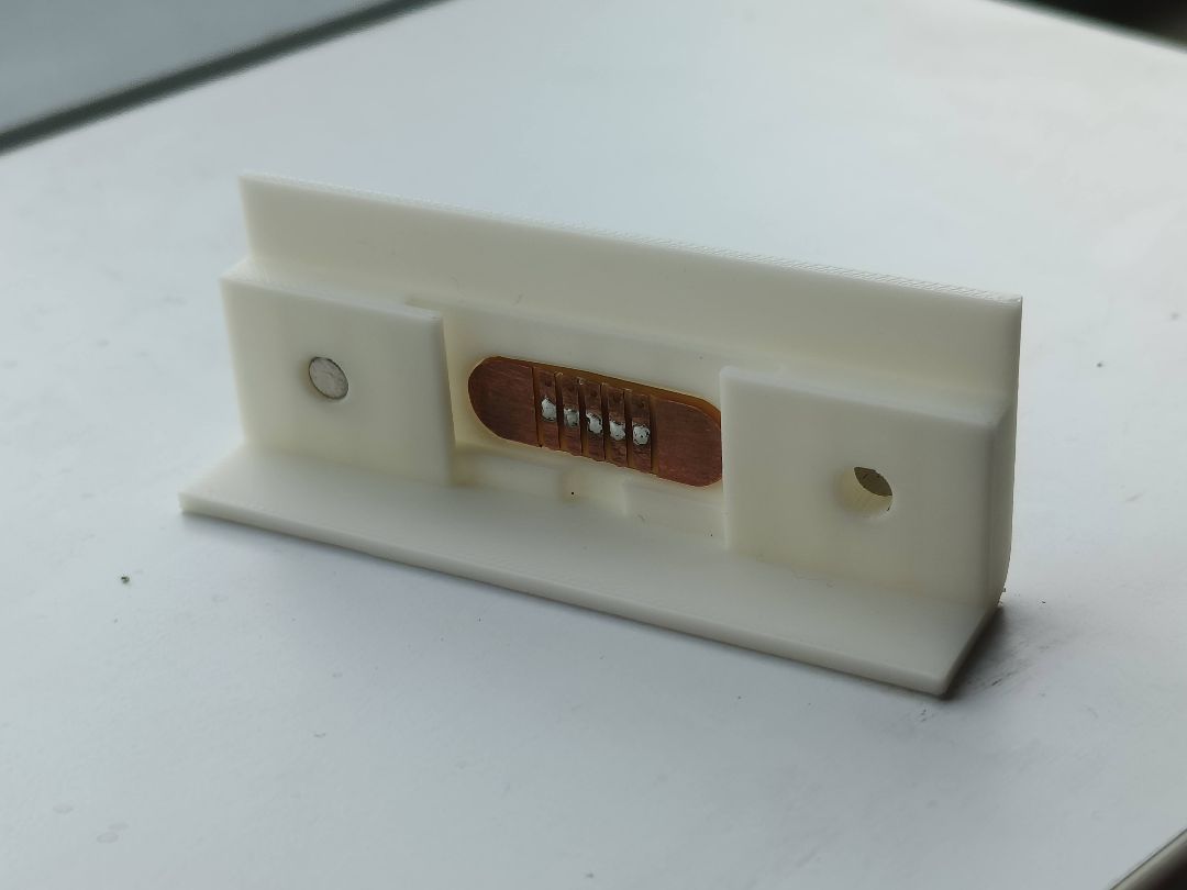
Connector PCB
I had to make a PCB that would sit underneath the module PCB to make connections or the pogo connector PCBs i
had made earlier. This PCB would actually as a connection point for the wires to be soldered on . A pinsocket will
be given on the side of the PCB that will face the bottom of the body of the module. This is given to make the
access to updi programming easier.
A mockup of the mounts were made to check if the connections sat correctly on the body.
The connection between the the keypad PCB and the connector PCB was good and the UPDI programming slot also came
out correctly.
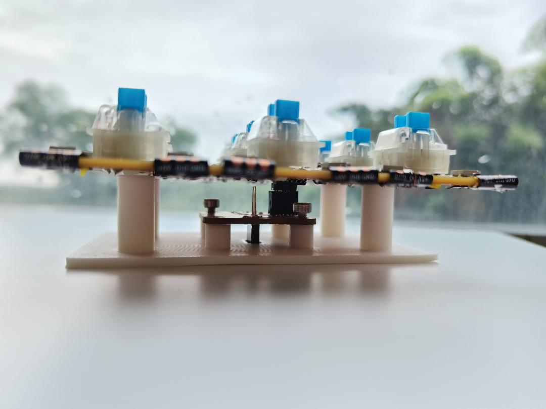
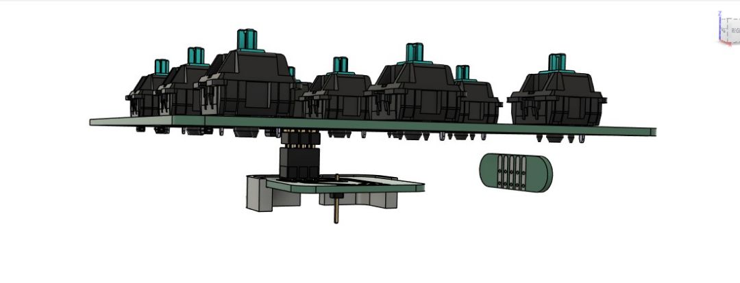
Assembly
I did a dry assemblky with all as all the elements required for the Node module were almost done. Everything was
assembeled properly.
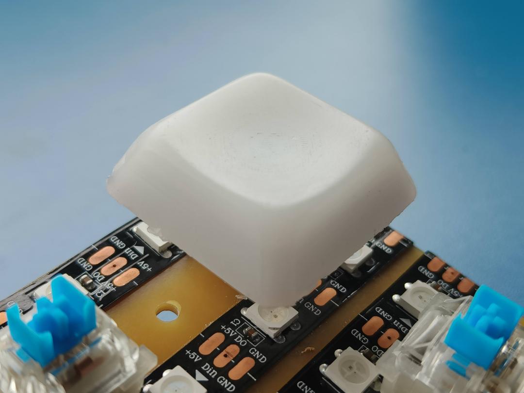
I lit up the keypad PCB with an example code from the Adafruit Neopixel library to see how the NOde module
looked with the lights on. The keycaps diffused the lights really well!
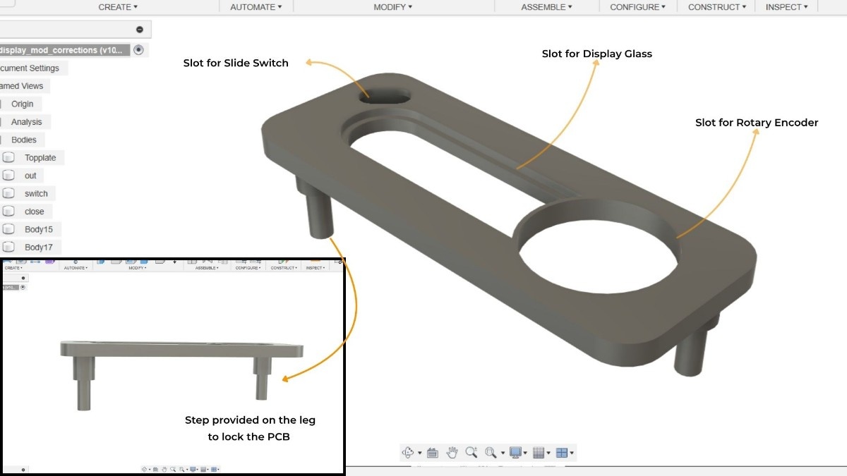
Making the Master
Module
CAD model
I went on to do the cad modeling of the body of the display mode. I made some mockups of the different design
details i wanted to visualize with the keypad modules.
The main parts of the body are : a screen, a on /off switch and a control knob.
The screen : the screen would be a .94" OLED display that would show the menu for the game.
On/off switch : A slide switch would be used to turn the entire product on or off . I wanted to sit the
switch at
an angle to mimic the style of a Gameboy console.
Control knob: A rotary encoder is provided to navigate between the games by turning the knob clockwise or
anti
clockwise
The challenge in this module was to accommodate the different height levels of the components and design the
model
accordingly.
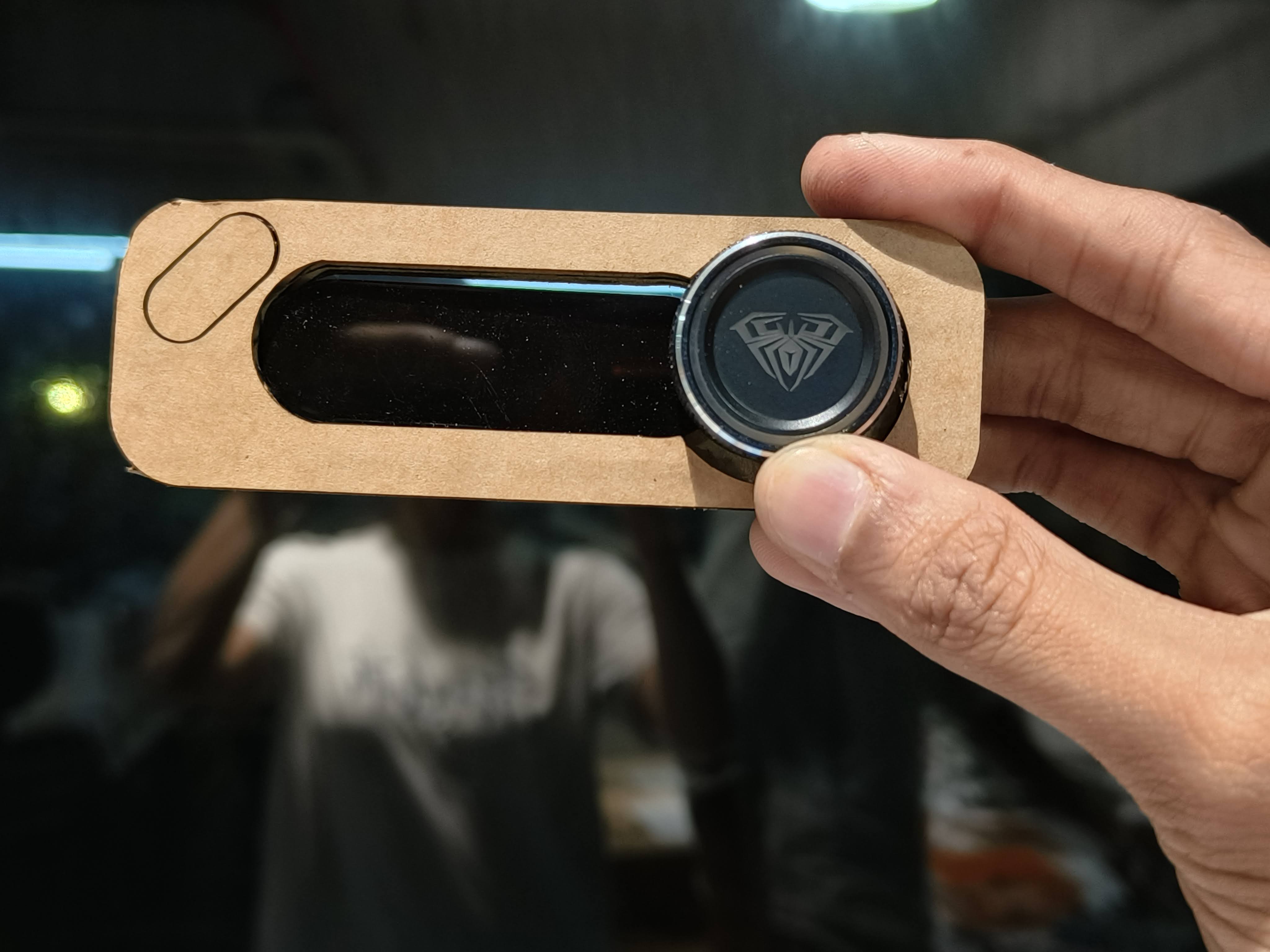
Design of the body
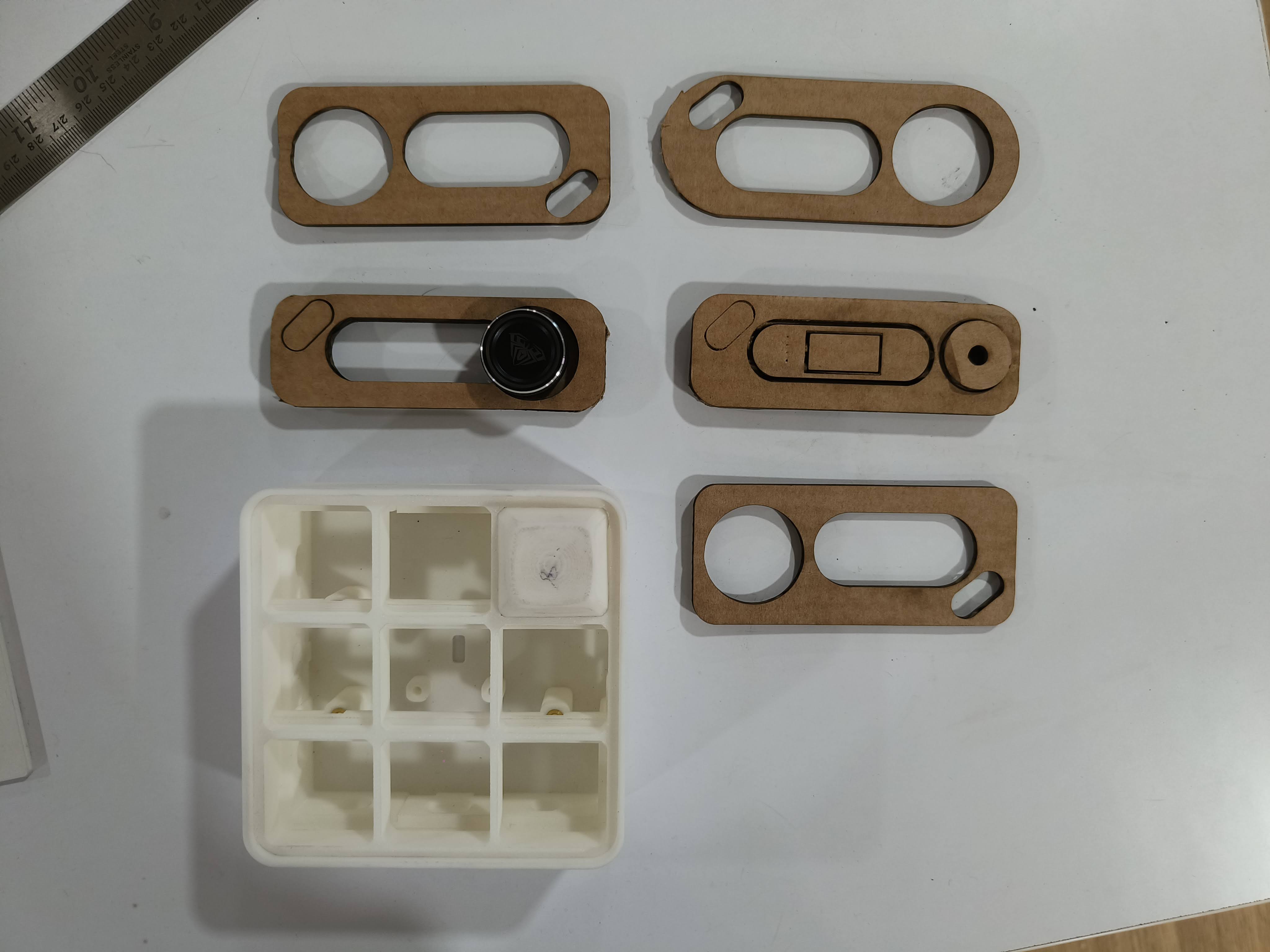
I made some mockups of the design of the toplate with cardboard to visulaize how each element will fit in with each other
At the end, this was the design i went ahead with as it looked visually balanced with all the elements placed well.
PCB Design and production
To arrange the components in a way that the heights are properly distributed proved to be a challenge.
The display had to be a height so that it could be visible through the acrylic. This will cause trouble to fit the
rotary encoder as it's knob is will stay very high from the surface which could not be adjusted . So we decided to
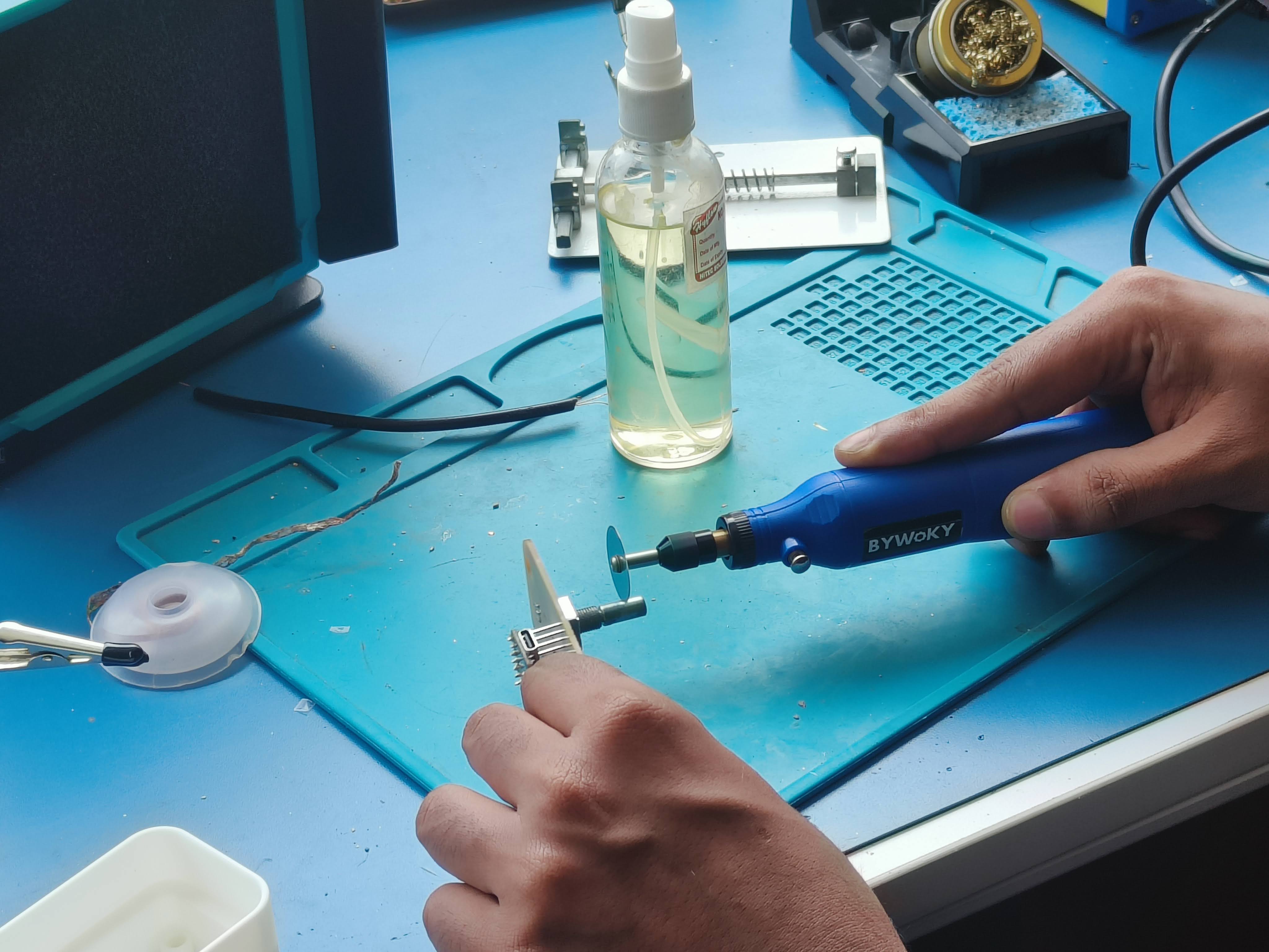
cut of the knob to a suitable height. Saheen helped to cut the knob using a dremel rotary tool.
Next challenge was to adjust the height at which the xiao ESP32C6 would sit beneth the PCB.
A set of Pinheaders had to the soldered on to the microcontroller,which was then fixed on the the board adjusting
it's height so as to fit correctly into the slot provided on the 3D print.
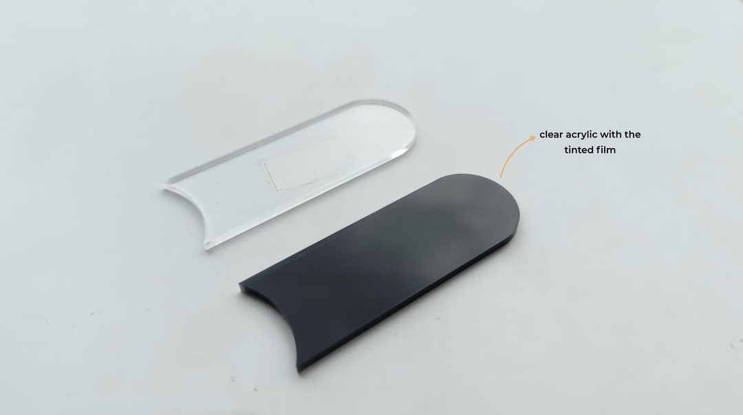
Laser cutting
The display glass was made in 1.8mm clear acrylic and cut to shape keeping the kerf values using the laser
cutting machine. I had to redo this step a few times to get the kerf correct. giving a 0.1mm offset seemed to be the best fit for my requirement.
A black semi transparent tinted sheet was then stuck on to the acrylic to give it the feel of a display
screen.
What's working? what's not?
The flexible PCBs required some corrections as .I felt that the diy pogo connectors could be improved upon
more. Even though the connection worked out well a
more effective way could be found.
The thickness of the body of the display module was little thicker than the body of the node. This caused a
issue with the connections of the pogo connectors. The pins were not touching the landing pad of the PCB. A
slight correction would help in that area for the connections to work out better.
The magnetic connection between the module may need more strength or the positon of the magnets needed to be
changed . Whenever the modules are lifted together quickly the module detatchh and fall apart.
The connector PCB had to be remade as the pad positions turned out to be wrong. This was because i got confused
when the board was flipped while making the KiCad layout. This has to be resolved.
What questions need to be resolved?
The biggest concern i have is whether the I2C connections would work properly. As there were issues coming up
with the ribbon cables and the pogo connectors makes me concerned with how the programming would go.
The programming seems to be quite complicated and as fixing the issues with the connections are quite time
consuming , I may face a time crunch during programming.
I may not be able to finsh 3 modules and an atomizer on time , so i will have to see how i can make progress in
that section
How many games can be programmed and could be played properly.
What will happen when?
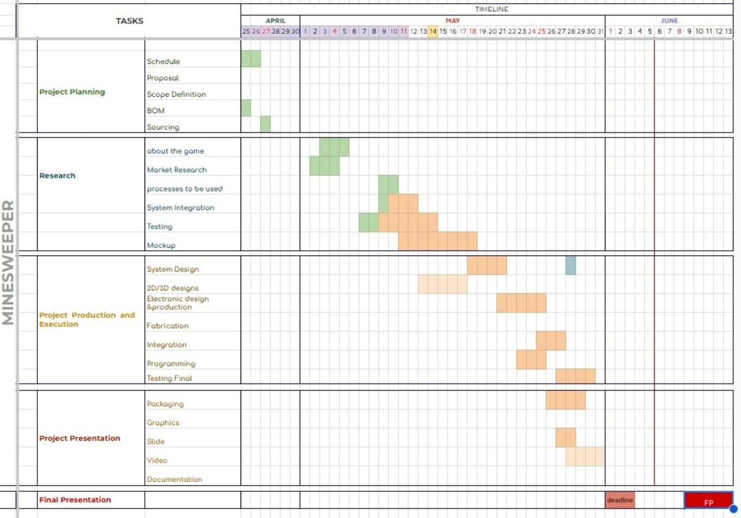
I have prepared a schedule to help me track my process and progress. I also made schedules for each week to help
in understanding whether tasks had gone past their timeline and to cover up that time by keeping buffers
accordingly.
Schedule
What have you learned?
Throughout the weeks I got to learn a lot about diverse fields that i had no prior experience in. To incorporate
all these learnings and compress it into one project has be challenging and fun at the same time. Documenting and
managing time to complete each task was another aspect that was inculcated within the project,
Specifically through this project i got to learn differnt ways to accomodate the electronics inside a product
and integrate and package it neatly.This will be very helpful as it helps me gain a in depth understanding of how
electronics can be integrated beautifully without it being an hassel while designing products.
I also got to learn how to make a product modular down to the electronics part. It makes my project easy to
replicate once one module is figured out.It also becomes customizable. In general the possibilities are endless
with this model of working.
Making the pogo connectors was intresting. It made me understand how expensive things could be made with easily
accessible tools by working with them creatively.
The flexible PCBs were an amazing addition to my project to negate the use of wires within the modules. Thanks
to Saheen, I got to explore this concept of using flexible PCBs as the wires making connections between the pogo
connector PCB and the connector hub PCB.
Even though it took some time, Molding and casting of the Keycaps truly showed the repeatability of using the
molds, which we couldnt explore during the assignment week.I was able to acheieve amazing and consistent surface
finish for each keycap
Overall, the main takeaway was to enjoy the process of learning!
 Next the led strips had to be fixed . I first cut the strip to the length of the pad. One led would have to be
removed because it won't be visible as it will be on the flip side of the board.
Next the led strips had to be fixed . I first cut the strip to the length of the pad. One led would have to be
removed because it won't be visible as it will be on the flip side of the board.
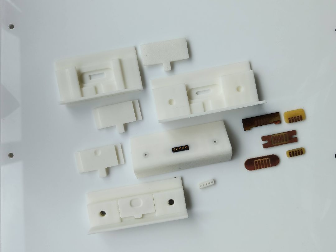
 Parts of the body was made to test out how the overall connections would work.

 It is then casted with epoxy resin. The finish and colour cme out pretty good. The resin did not reach
every surface so i am trying to achieve a proper finish now.
It is then casted with epoxy resin. The finish and colour cme out pretty good. The resin did not reach
every surface so i am trying to achieve a proper finish now.