
Electronics Design
This week, I explored PCB design and fabrication, focusing on schematic creation, component selection, routing, and debugging. I used KiCad for schematic and PCB design, experimenting with different routing strategies and design rules.
Learning Objectives
Assignments
Group Assignments
Individual Assignments
Group Assignment
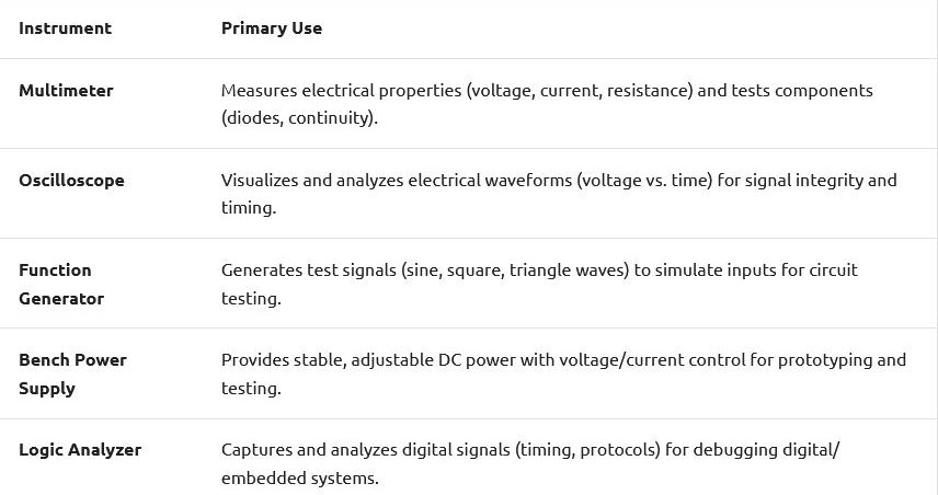
In this group assignment, we used various test equipment to analyze the operation of a microcontroller circuit board. We began by verifying the power supply using a multimeter to ensure the board received a stable voltage. An oscilloscope was then used to check clock signals, confirming the correct operation of the system's timing components. Additionally, GPIO pins were observed to monitor their state changes, helping us understand the behavior of digital outputs.
Group AssignmentMy primary focus was on using the logic analyzer to examine communication protocols. I connected the analyzer to the microcontroller's I2C and UART lines, capturing real-time signals as data was transmitted between the microcontroller and peripherals. Using protocol decoding, I was able to interpret the transmitted data, checking for errors and validating the correct operation of communication interfaces. This step was crucial in debugging and ensuring that the microcontroller properly interacted with external devices.
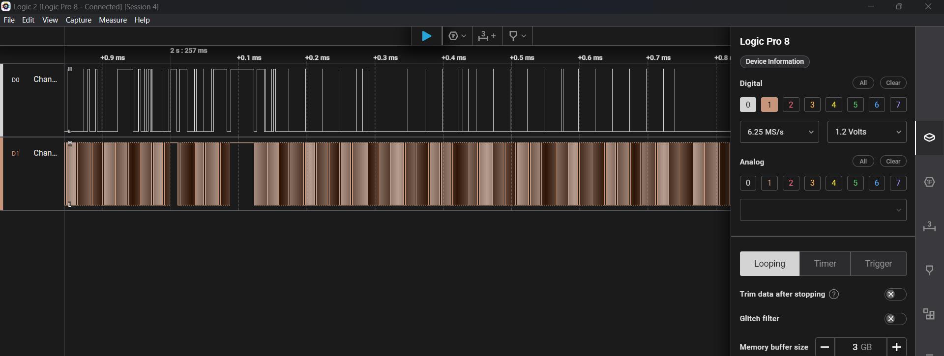
Through this hands-on experience, I gained valuable insights into debugging embedded systems. The logic analyzer provided a deeper understanding of how data is structured and transmitted, reinforcing the importance of signal integrity and timing analysis in microcontroller-based circuits. This assignment helped us develop practical troubleshooting skills and a systematic approach to diagnosing electronic circuits.
Electronic Components
Electronic components are the elements of the circuit which help in its functioning the electrical circuit. Electronic components are the basic building blocks of an electronic circuit any electronic system or any electronic device. They can control the flow of electrons in an electronic system or electronic circuit.
Types of Electronic Components
An electrical circuit is an interconnection of Electronic Components. Based on their capability to generate energy these elements are classified into active or passive electronic Components.
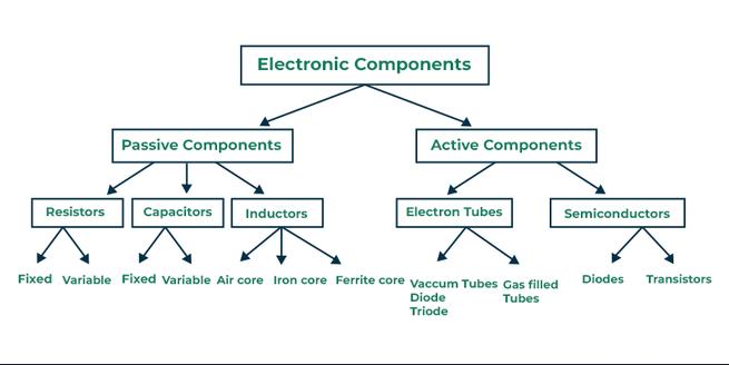
Photo credit: geeksforgeeks
Electronic Components are classified into two groups:
- Passive Components:
Passive components are electronic devices that don't need an external power source to operate actively. They mainly resist, store, or control the flow of electric current or voltage in a circuit without actively amplifying or generating signals. For eg. Resistors, Capacitors, Transformers, Diodes, Thermistors, etc.
- Active components
Active components are electronic devices that need an external power source to work. They actively control and manipulate the flow of electric current in a circuit. These components can amplify, switch, or generate electrical signals. For eg. Diode, Transistor, Integrated circuit, etc.
Connectors
Electronic connectors are devices that join electronic circuits. They are used in assembling, installing, and supplying power to electrical devices. Connectors are an important component of electronics used in industrial machinery, consumer products, communications, and home appliances.
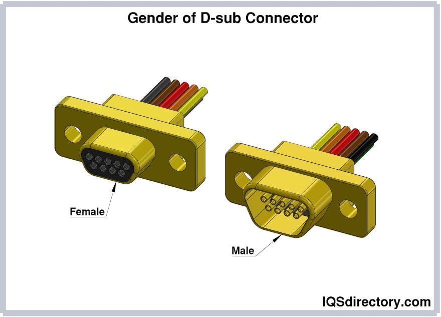
Photo credit: IQSdirectory
For electronic connectors, gender is used to differentiate the mating connectors that match together in size, shape, and number of pins. The plug or male connector has pins for connecting to the female connector, which has a receptacle, jack, or socket for the male pins. The female connector has socket holes that contain terminals to wires, cables, or devices. The pins of the male plug are inserted into the female jack or socket to make electrical connections.
We explored different types of electronic connectors. The types of electronic connectors are:
-
Header Connectors
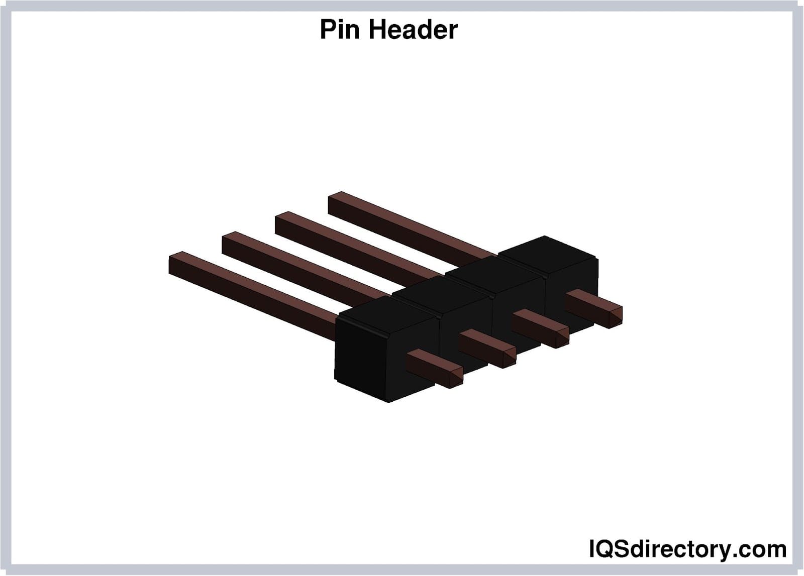
Header Pins Photo credit: IQSdirectory
Cables made to connect to these pin headers are usually one of two types: individual wires with crimp connectors on them or ribbon cables with insulation displacement connectors.

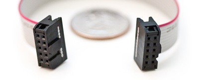
Photo credit: IQSdirectory
-
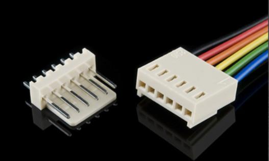
JST Connectors
Gender of Connectors Photo credit: IQSdirectory
Japanese Solderless Terminal, also referred to as JST, is manufactured by a Japanese company of the same name. The JST system is primarily designed to bridge electrical connections or carry an electrical signal.
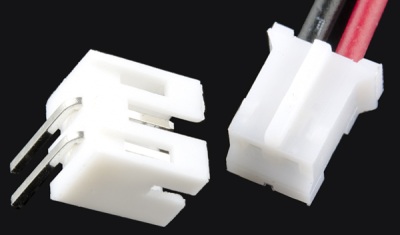
- Dupont
Barrel Connectors Photo credit: Core Electronics
-
Molex Connectors
Molex Connectors Photo credit: IQSdirectory
-
Barrel Connectors
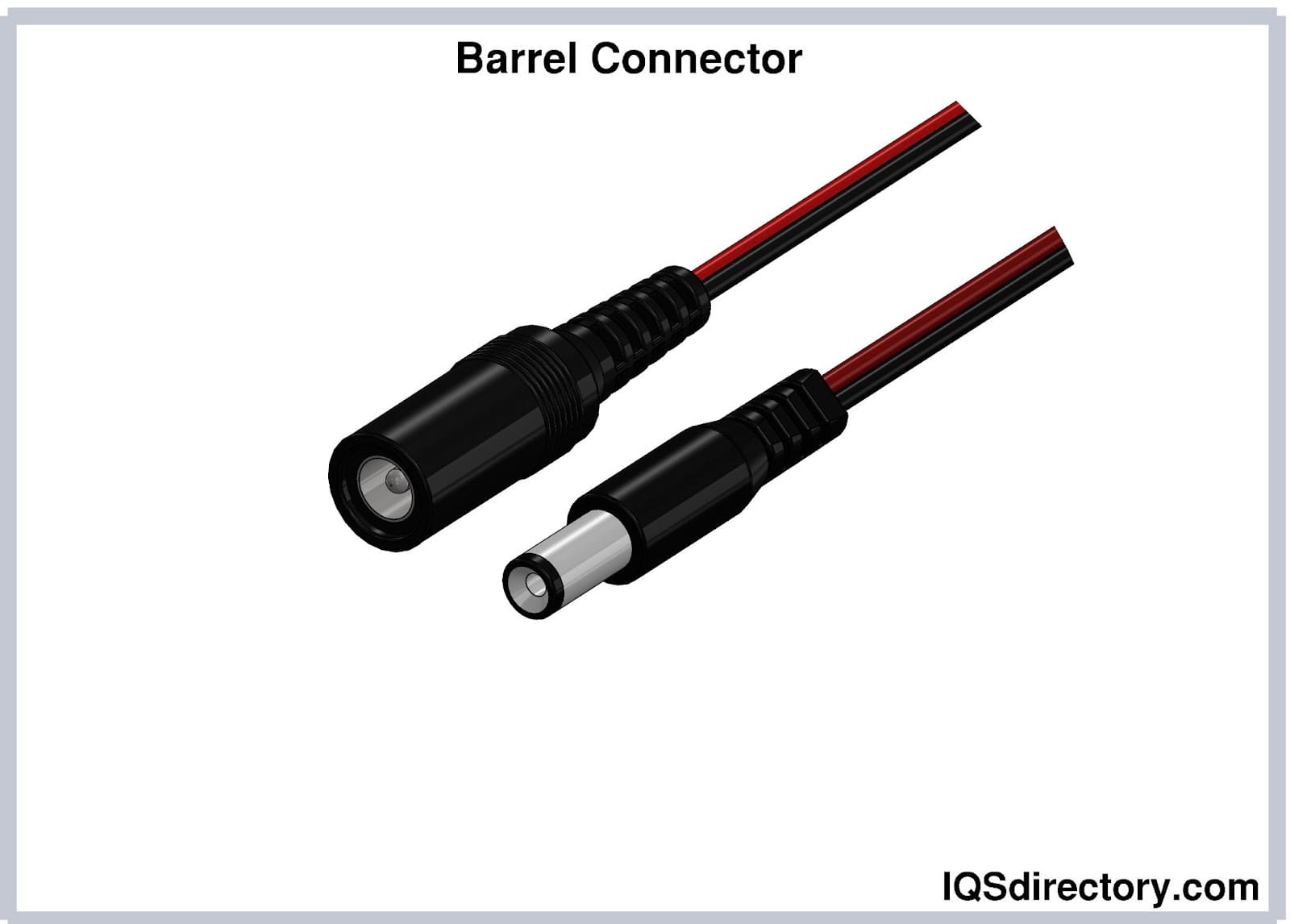
Barrel Connectors Photo credit: IQSdirectory
-
Terminal Connectors
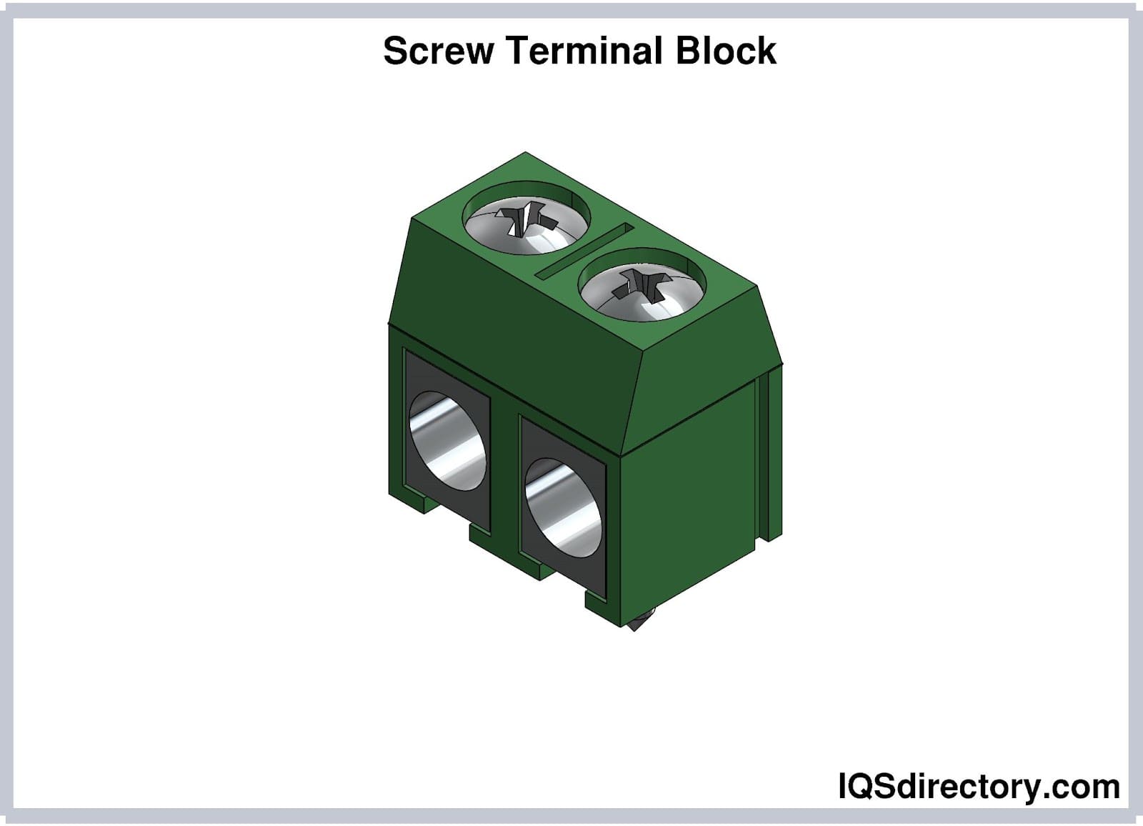
Screw Terminal Photo credit: IQSdirectory
-
USB Connectors
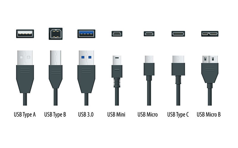
Types of USB Connectors Photo credit: Apple
Circuits
Pull Up Resistor
Pull-up resistors are resistors which are used to ensure that a wire is pulled to a high logical level in the absence of an input signal.
Digital logic circuits have three logic states: high, low and floating (or high impedance). The high-impedance state occurs when the pin is not pulled to a high or low logic level, but is left “floating" instead.
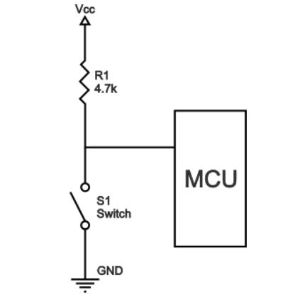
Photo credit: eepower
Without the pull-up resistor, the MCU’s input would be floating when the switch is open and pulled down to a logical low only when the switch is closed.
Pull Down Circuit
Pull-down resistors are resistors which are used to ensure that a wire is pulled to a low logical level in the absence of an input signal.
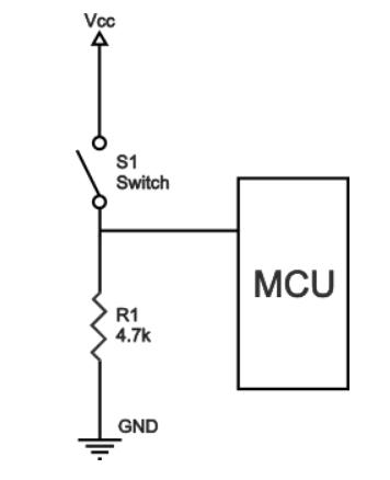
Photo credit: eepower
When the pushbutton is not pressed (open) the state of the pin will be logic LOW and when the pushbutton is pressed (closed) the state will be logical HIGH.
The pull-down resistor must have a larger resistance than the impedance of the logic circuit, or else it might be able to pull the voltage down by too much and the input voltage at the pin would remain at a constant logical low value - regardless of the switch position.
I have refered this webpage for the content and learning of pull up and pull down resistors
Pull Up Pull Down ResistorsVoltage Divider Circuit
A voltage divider involves applying a voltage source across a series of two resistors. The primary purpose of this circuit is to scale down the input voltage to a lower value based on the ratio of the two resistors.
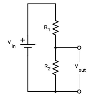
Photo credit: All about circuits
I have refered the below linked webpage for the content for Voltage Divide Circuits.
Voltage Divider CalculatorThe poterntiometer is the most common application of a voltage divider circuit. A potentiometer usually has three external pins: two are the ends of the resistor and one is connected to the wiper arm.
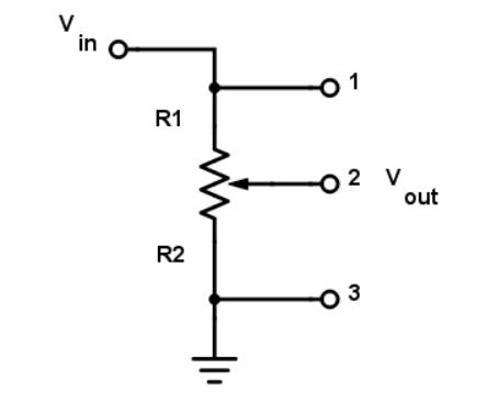
Photo credit: All about circuits
A Level Shifter is another application of a voltage divider circuit,when a voltage needs to be leveled down. The most common scenario is when interfacing signals between a sensor and a microcontroller with two different voltage levels.
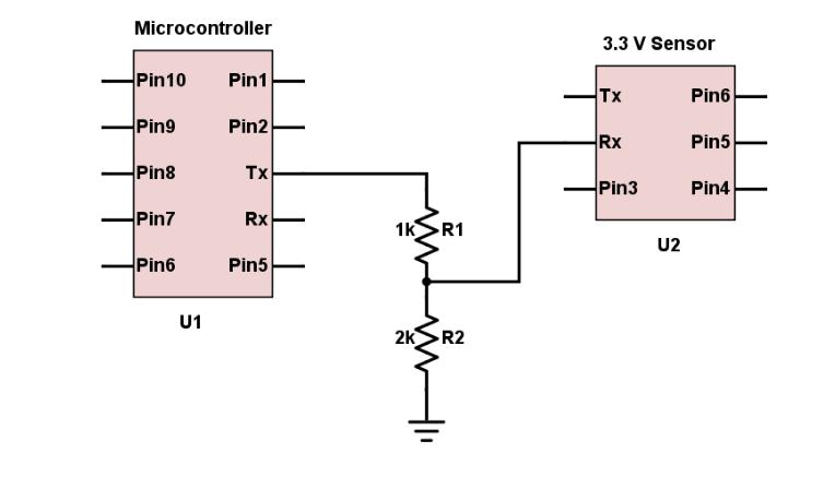
Photo credit: All about circuits
Voltage Regulator
Photo credit: Flipkart
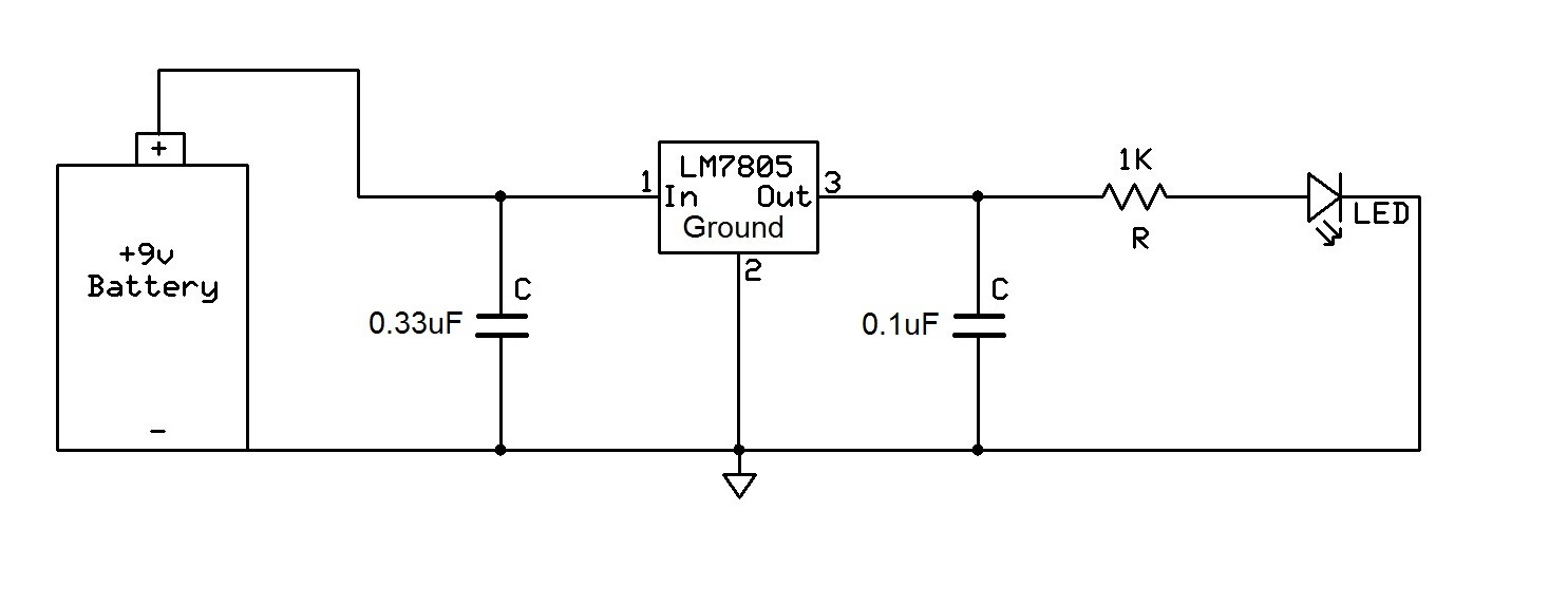
Photo credit: Learning about electronics
I have refered the below linked webpage for the content for Voltage Regulator Circuit and how to connect it in a circuit.
Learning about electronicsTo integrate a voltage regulator into a circuit properly, capacitors are added to filter out noise and stabilize the voltage. The first capacitor, a 0.33µF ceramic capacitor, is placed between the voltage source (e.g., a 9V battery) and the input pin of the regulator. This capacitor helps filter out unwanted noise or AC ripple from the power supply, ensuring that a clean DC voltage enters the regulator. By acting as a bypass capacitor, it diverts any high-frequency noise to ground, improving the efficiency of the regulator.
The second capacitor, a 0.1µF ceramic capacitor, is connected to the output pin of the regulator. This capacitor smooths out any remaining fluctuations or high-frequency noise in the regulated 5V output. While this may not be critical for simple applications like powering an LED, it becomes essential when supplying power to logic circuits or microcontrollers that require precise and stable voltages to function correctly. By following this setup, you ensure that the regulator operates efficiently and provides a clean, reliable power supply for your circuit.
EDA
Electronic Design Automation, or EDA, is a market segment consisting of software, hardware, and services with the collective goal of assisting in the definition, planning, design, implementation, verification, and subsequent manufacturing of semiconductor devices, or chips. Regarding the manufacturing of these devices, the primary providers of this service are semiconductor foundries, or fabs. These highly complex and costly facilities are either owned and operated by large, vertically integrated semiconductor companies or operated as independent, “pure-play” manufacturing service providers.
I refered the following webpage for the content of EDA and its definition.
Synopsys Electronic Design Automation is primarily a software business. Very sophisticated and complex software programs function primarily in one of three ways to assist with the design and manufacture of chips:- Simulation tools take a description of a proposed circuit and predict its behavior before is it implemented.
- Design tools take a description of a proposed circuit function and assemble the collection of circuit elements that implement that function. This is both a logical process (assemble and connect the circuit elements) and a physical process (create the interconnected geometric shapes that will implement the circuit during manufacturing). These tools are delivered as a combination of fully automated and interactively guided capabilities.
- Verification tools examine either the logical or physical representation of the chip to determine if the resultant design is connected correctly and will deliver the required performance.
Some examples of EDA softwares are KiCad, Autodesk Eagle, Cadence, Altium,etc.
KiCad
KiCad is an open source software suite for Electronic Design Automation (EDA). The programs handle Schematic Capture, and PCB Layout with Gerber and IPC-2581 output. The suite runs on Windows, Linux and macOS and is licensed under GNU GPL v3.
KiCad Download PageI tried to explore KiCad for this week as my EDA tool because it is Open Source, packed with features and lots of shortcuts
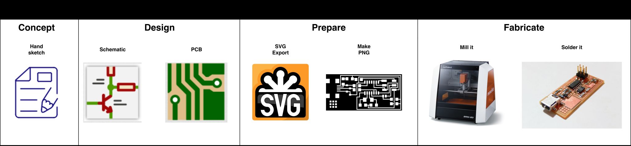
Photo credit: Fablab Docs
KiCad's Schematic Editor supports everything from the most basic schematic to a complex hierarchical design with hundreds of sheets. Create your own custom symbols or use some of the thousands found in the official KiCad library.
KiCad's PCB Editor is approachable enough to make your first PCB design easy, and powerful enough for complex modern designs.
KiCad's 3D Viewer allows easy inspection of your PCB to check mechanical fit and to preview your finished product.
Essential Concepts for PCB Design
Designing a Printed Circuit Board (PCB) involves translating a circuit schematic into a physical layout while ensuring manufacturability, signal integrity, and reliability. Below are key elements to understand before starting a PCB design.
Schematic Design
- Schematic Symbol: A graphical representation of a component used in circuit diagrams (e.g., a resistor is a zigzag line, a capacitor is two parallel lines).
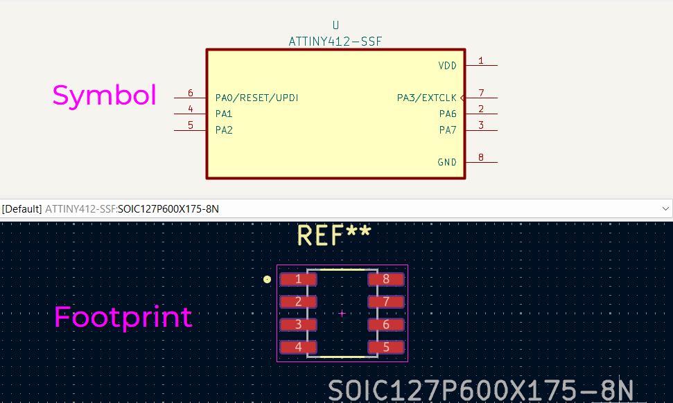
3D Viewer - Footprint: The actual physical layout of a component on the PCB, showing pad locations for soldering.
- Component Libraries: EDA tools provide predefined symbols and footprints (KiCad, Eagle, Altium, etc.), or they can be custom-made.
Traces & Routing
Traces are copper pathways on a PCB that electrically connect components. Proper routing ensures circuit reliability.

- Trace Width: Determines how much current a trace can carry. Wider traces are used for high-current paths.
- Trace Clearance: The minimum gap between two traces to prevent short circuits.
- Routing: Manual or autorouting strategies to optimize signal paths.
Design Rules and Checks
Ensuring a PCB follows proper electrical and manufacturing guidelines is crucial.
- DRC (Design Rule Check): Checks for trace width, clearance, via sizes, and other manufacturing constraints.
- ERC (Electrical Rule Check): Detects issues like unconnected nets, incorrect pin connections, and missing power connections.
Individual Assignments
Design a Development Board Using a EDA tool
For this week's assignment, we worked with Electronic Design Automation (EDA) tools to create a custom circuit. The goal was to design a development board using available components while ensuring proper routing and design rule compliance
Designing a basic circuit in KiCad
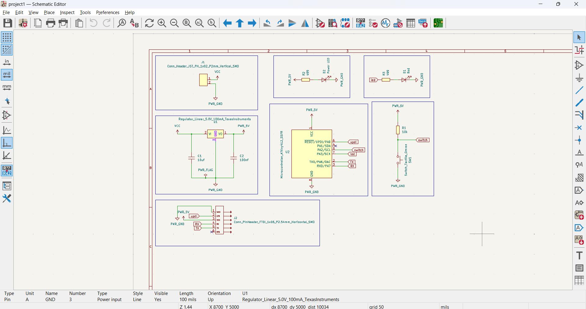
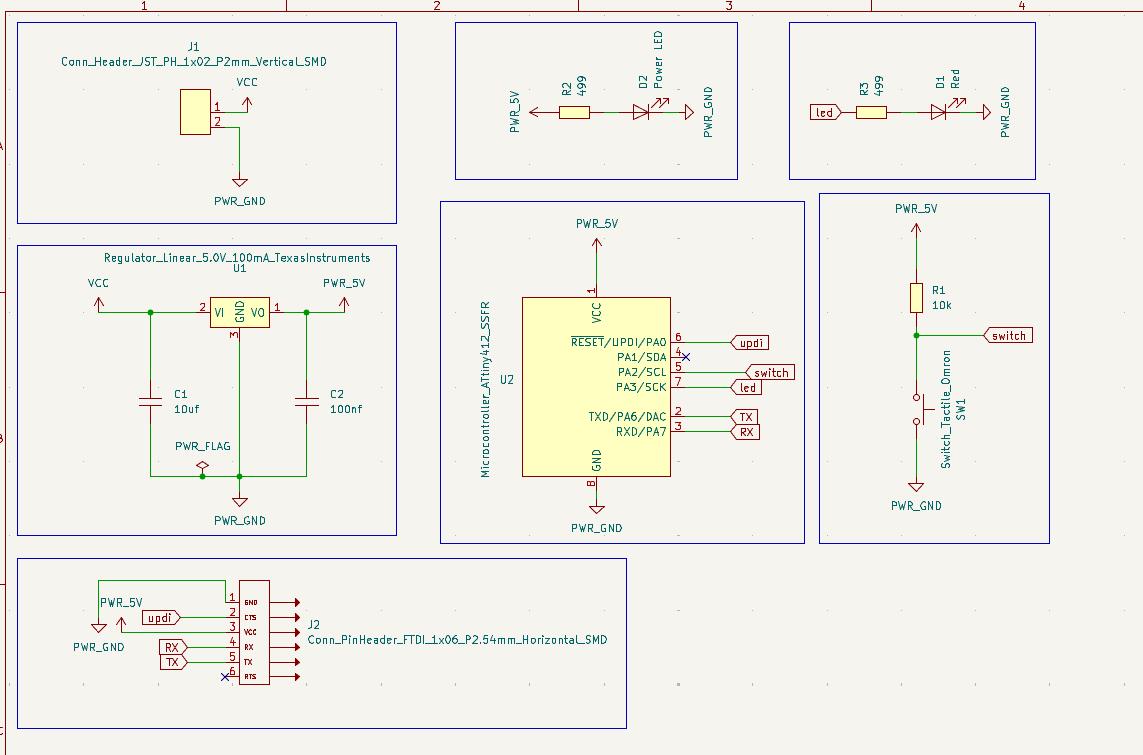
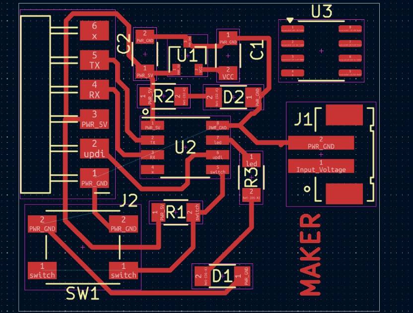
We started with a basic circuit in KiCad with components like a Attiny 412, a pair of LEDs, push button and voltage regulator to understand the workflow of the KiCad EDA.
There was a initial class by Midhun, FabAcademy 24 Student and Technology Fellow about the basics of using KiCad and making a development board using Attiny 412. Everyone built this basic Schematic and PCB as part of this class.
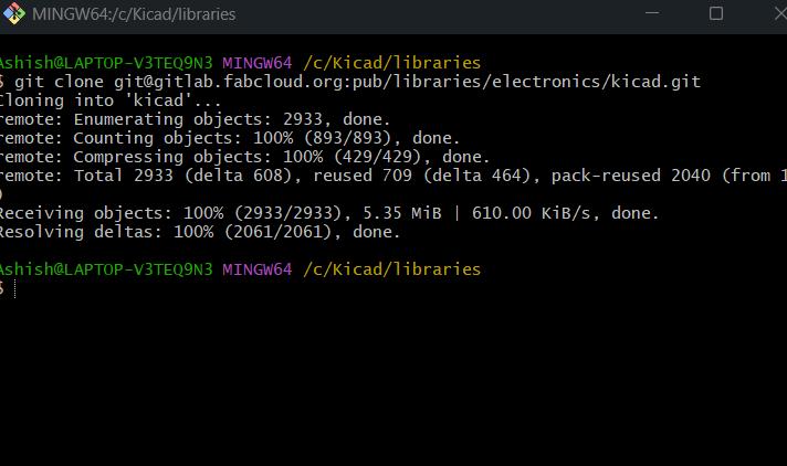
Before we start designing, we need to clone the fab library of devices for KiCad into our Personal Computer system. You can find the library on the below link
Fab KiCad Library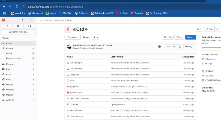
Follow these instructions provided in the readme file of the repository
- Clone or download this repository. You may rename the directory to fab.
- Store it in a safe place such as ~/kicad/libraries or C:/kicad/libraries.
- Run KiCad or open a KiCad .pro file.
- Go to "Preferences / Manage Symbol Libraries" and add fab.kicad_sym as symbol library.
- Go to "Preferences / Manage Footprint Libraries" and add fab.pretty as footprint library.
- Go to "Preferences / Configure Paths" and add new environment variable "FAB" that points to location of the fab library on your drive, e.g. ~/kicad/libraries/fab. This is needed for the 3D models to load correctly.
After cloning the repository, as said in the instructions there are three important steps: Configuring PATH, Adding Symbol Library and Adding Footprint Library
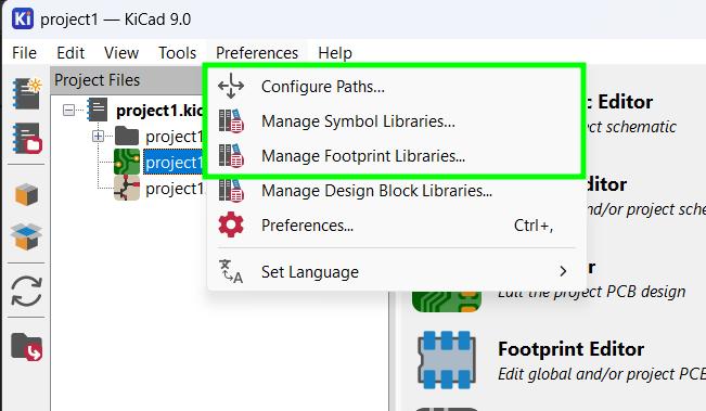
Add the symbol and footprint library as mentioned in the instructions above. You'll be able to access the fab component symbols and footprints only after adding the libraries properly.
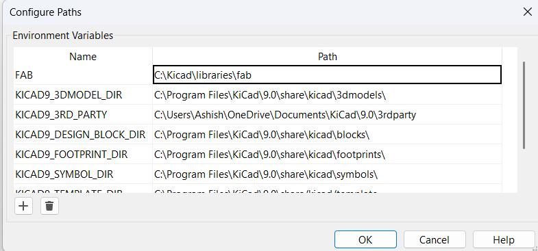
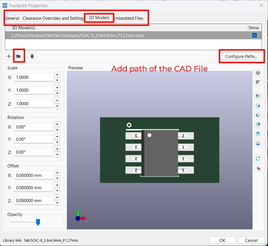
Make sure to add the path to the environment variable, as skipping this step would result in failing to fetch the 3d Models of the devices. We didn't initially do this step, therfore we had to manually add the path to each component to fetch the individual 3D models
Adding 3D Models to footprints manuallyThe CAD files can be manually added for footprints in the PCB Editor window by selecting the properties of the footprint.
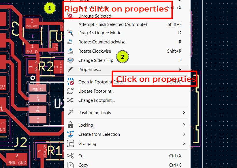
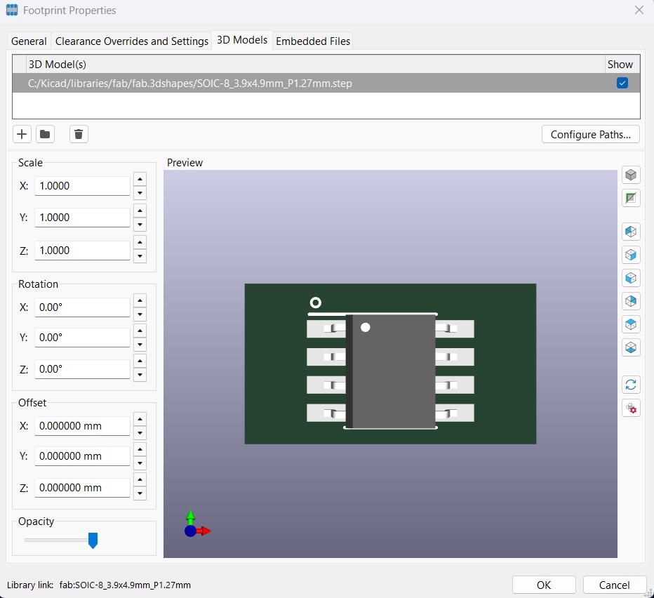
The footprint properties window has a 3D Models tab wherein you can add path to CAD File and adjust the CAD Properties such as it's location,orientation and offset.
Now we are all set to begin designing our circuit, we followed the above steps to include the devices library from the fablab inventory directly into our KiCad Workflow. Now I'll show you the different steps we need to take to build this circuit.
Adding external components from SnapEDA
In addition to the fab library, we can also add components from external libraries such as SnapEDA. SnapEDA is a free online library of electronic components that provides symbols, footprints, and 3D models for various EDA tools.

We can search for the components we need in the SnapEDA library by typing their names in the search bar. For example, we can search for the Attiny 412 SSF component in the SnapEDA library.
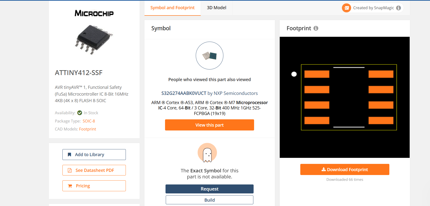
After finding the component, we can download the symbol, footprint, and 3D model files from SnapEDA. We can then import these files into KiCad by using the "Import Symbol" and "Import Footprint" tools.
Designing Workflow
In this section, I will explain the different steps we need to take to build a circuit in KiCad. The steps are as follows:
Adding Components
To add components to the schematic, we need to open the Schematic Editor in KiCad. The Schematic Editor is where we can create and edit our circuit diagrams. We can add components from the library by using the "Add Symbol" tool or by pressing the shortcut key 'A'.
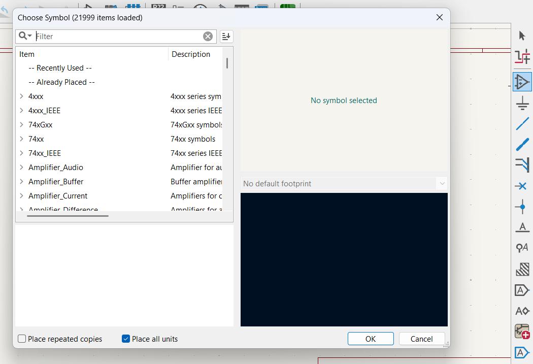
We can search for the components we need in the library by typing their names in the search bar.
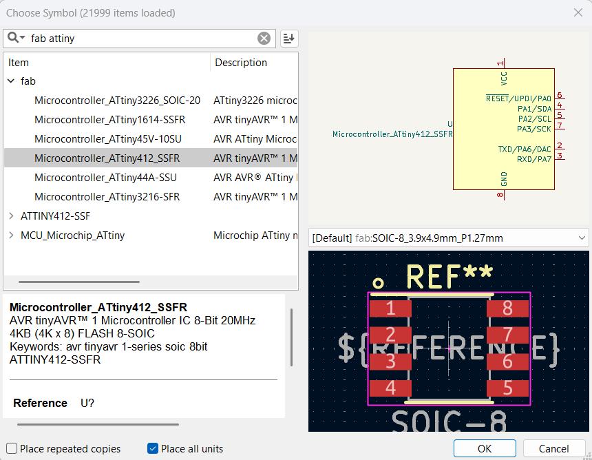
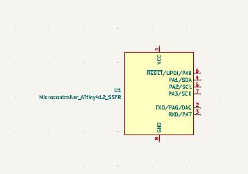
I added the Attiny 412 from the fab library that we cloned earlier. The Attiny 412 is a small microcontroller that is commonly used in embedded systems. It has 4KB of flash memory, 256 bytes of SRAM, and 256 bytes of EEPROM. It also has 6 GPIO pins, which can be used for input or output.
After adding the Attiny 412, we can add other components such as LEDs, resistors, capacitors, and push buttons. We can also add power and ground symbols to the schematic.
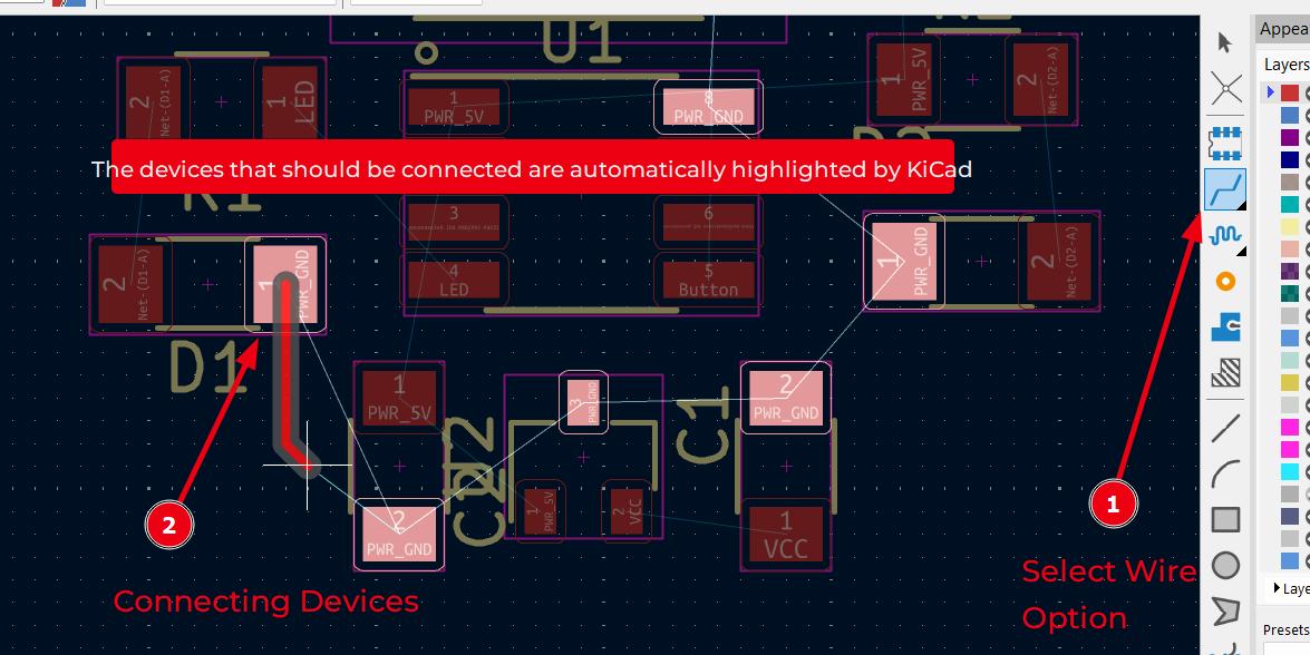
Connecting components with wires
After adding the components, we need to connect them with wires. We can use the "Place Wire" tool or press the shortcut key 'W' to draw wires between the components. We can also use the "Place Junction" tool or press the shortcut key 'J' to create junctions where wires intersect.
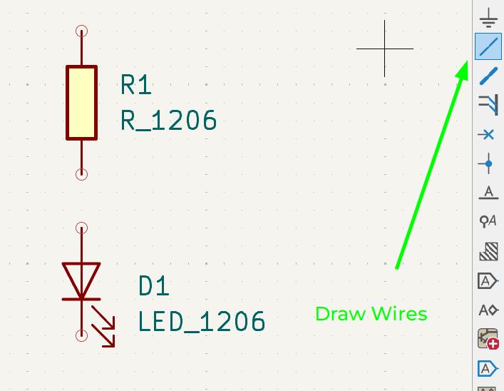
To connect the components, we can click on the pins of the components and drag the wire to the other component's pin. We can also use the "Place Junction" tool to create junctions where wires intersect. The junctions are represented by small circles in the schematic.
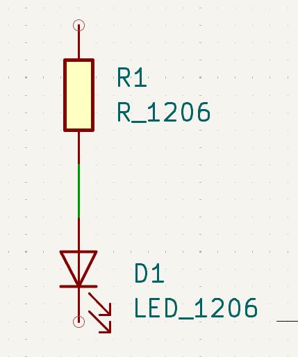
After connecting the components, we can see the wires in the schematic. The wires are represented by lines that connect the pins of the components. We can also see the junctions where the wires intersect. The junctions are represented by small circles in the schematic.
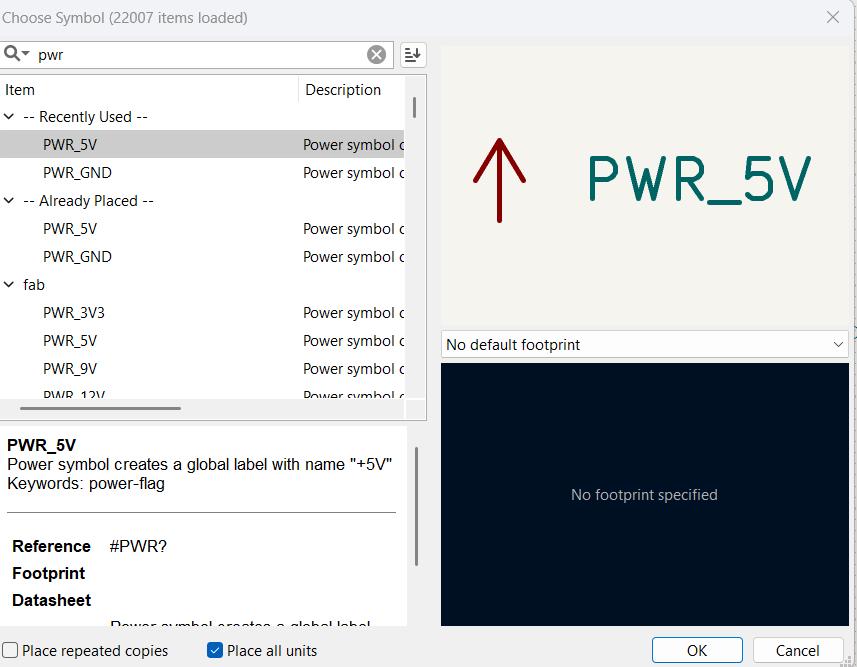
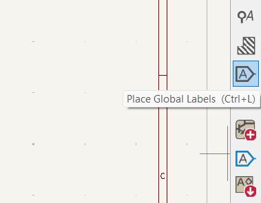
Adding Global Labels
Global labels are used to connect different parts of the circuit that are not physically connected but logically connected. They are useful for connecting components that are far apart in the schematic or for connecting components that are on different sheets of the schematic.
To add a global label, we can use the "Place Global Label" tool or press the shortcut key 'G'. We can then click on the wire where we want to place the label and type the name of the label. The label will be represented by a small rectangle with the name inside it.
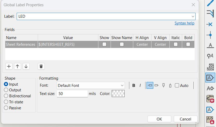
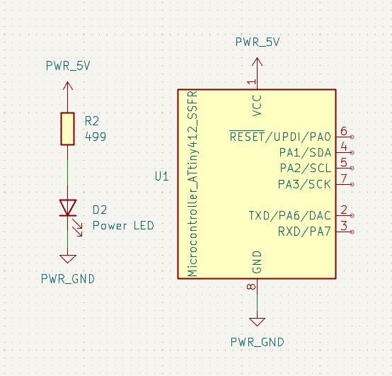
We can add global labels to connect the power and ground lines to the components. For example, we can add a global label called "PWR_5V" to connect the 5V power line to all the components that require 5V power. We can also add a global label called "GND" to connect the ground line to all the components that require ground.
We can also add global labels to connect the push button switch to the Attiny 412. For example, we can add a global label called "Button" to connect the push button switch to the Attiny 412's GPIO pin.
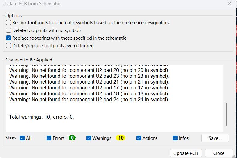
Running the ERC
After completing the schematic, we need to run the Electrical Rule Check (ERC) to ensure that there are no errors or warnings in the circuit. The ERC checks for unconnected pins, missing connections, and other potential issues in the schematic.
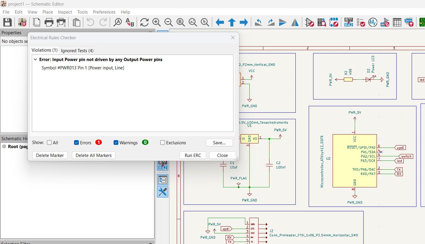
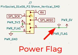
I found a error on the ERC, Input Power not driven by any Output Power pins. This is a common error found. The error shows up when the Power and Ground Lines are not detected by the ERC as Power lines. To resolve this issue, we have to add a PWR Flag to anyone of the many PWR lines. For eg. If I have added a PWR_5V at different places, it's only necessary to add one power flag at at ony one of the PWR_5V lines.
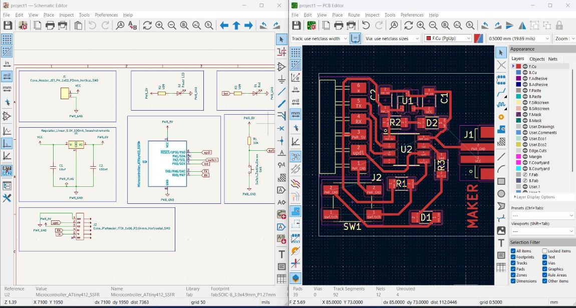
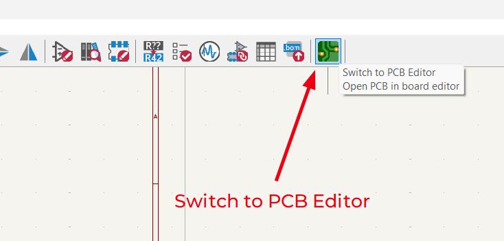
Converting Schematic to PCB Design
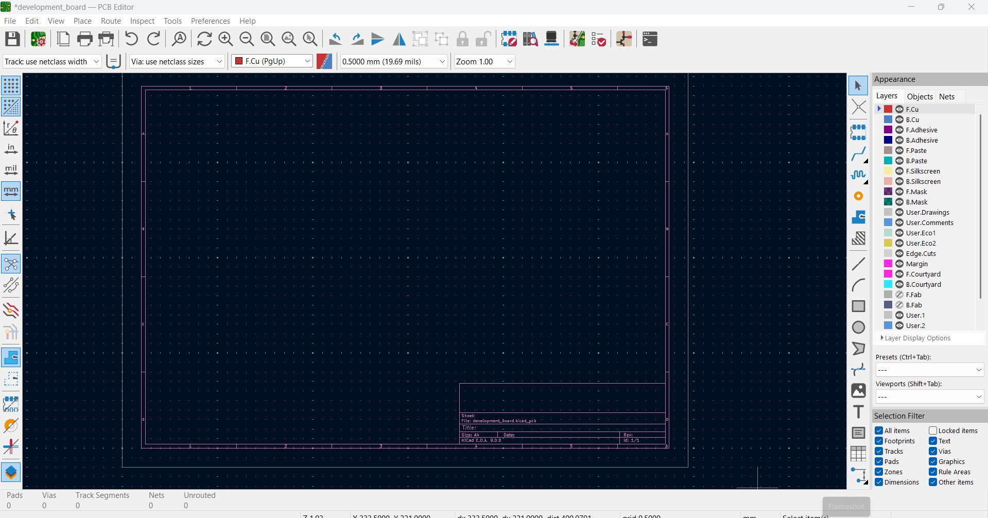
After completing the schematic and running the ERC, we can convert the schematic to a PCB design. We can do this by clicking on the "PCB Editor" button in the toolbar or by pressing the shortcut key 'F9'. This will open the PCB Editor window where we can create the PCB layout.
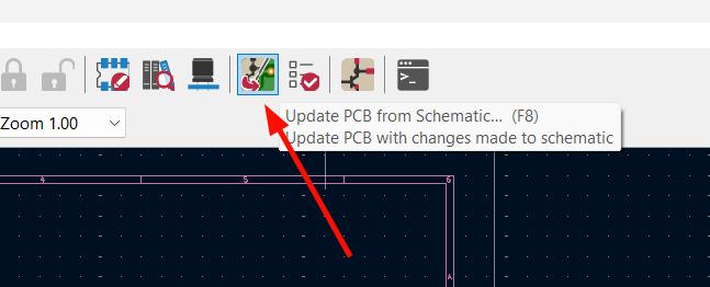
Update the PCB from the schematic by clicking on the "Update PCB from Schematic" button in the toolbar or by pressing the shortcut key 'F8'. This will update the PCB layout with the components and connections from the schematic.
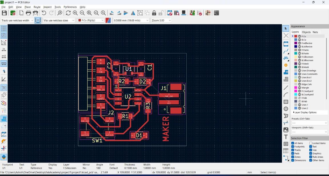
In the PCB Editor, we can see the components that we added in the schematic.
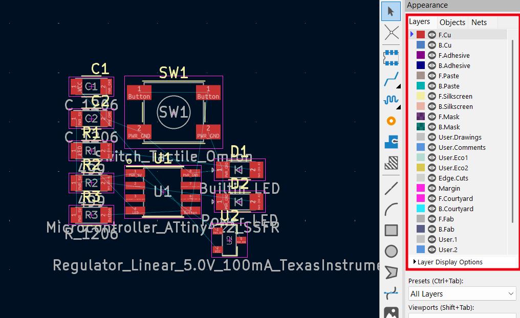
We can also see the different layers of the PCB, such as the copper layer, silkscreen layer, and solder mask layer. The copper layer is where the traces are routed, the silkscreen layer is where the component labels and logos are printed, and the solder mask layer is where the pads for soldering components are located.
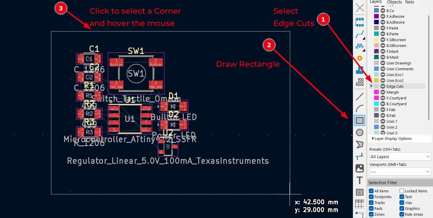
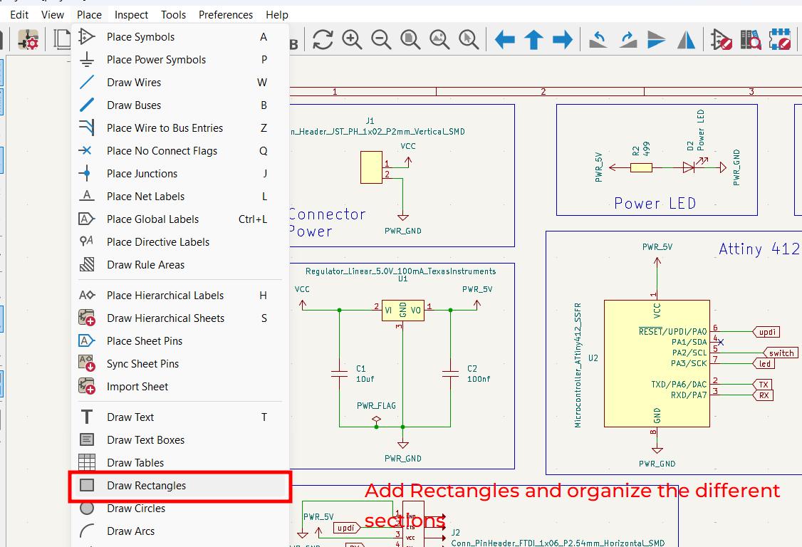
We can also add a bounding box to the PCB layout to define the size and shape of the PCB. The bounding box is represented by a rectangle that encloses the components and traces on the PCB. We can add the bounding box by using the "Place Rectangle" tool or by pressing the shortcut key 'R'.
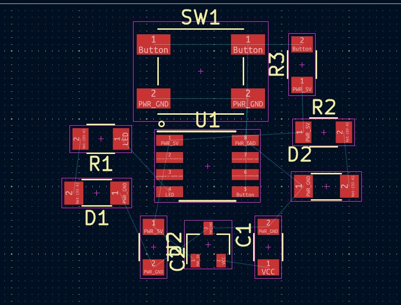
After adding the bounding box, we can arrange the components on the PCB layout for easier tracing. We can move the components around by clicking and dragging them to the desired location. We can also rotate the components by right-clicking on them and selecting "Rotate" or by pressing the shortcut key 'R'.
Setting Design Rules
Design Rules are required to constraint the traces and different parameters according to the capabilities of the PCB router and required features. It helps to standardize the parameters of the PCB like minimum track width, track clearance, etc.

The design constraints can be set from the Board Setup option found on the toolbar in the PCB Design Window. The Constraints can be set under the Design Rules section of the Board Setup. You can also import the Settings from Another Board
The above given constraints were provided by our instructors according to the PCB Milling Router available in our Lab.
Adding Traces
After arranging the components for easier tracing we have to connect them using the Trace option. You can either select the Route Single Tracks option or the X key as shortcut
- X - Select Single Wire Trace
- D - Adjust the Traces after they are Done
- M - Move components (Traces don't follow the movement)
- G - Move components (Traces adjust according to movememnt of components)
The G Shortcut has some limitations, if the traces overlap another component the movement cann
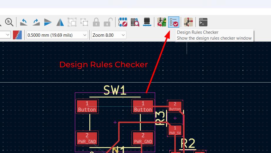
Running DRC
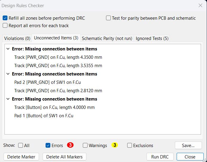
The DRC button can be found on the tool bar in the PCB Editor Window. The DRC and ERC buttons look similar. The ERC is only available in the SChematic Editor , while DRC is available in PCB Editor
The DRC showed some errors and warnings. The warnings given under the Unconnected items are for the Push button switch. The pushbutton terminals are internally connected, therefore it is not required to connect them in the board. This is a common error for push buttons.
The other common errors that i faced was unconnected pins, which I overlooked while connecting traces.
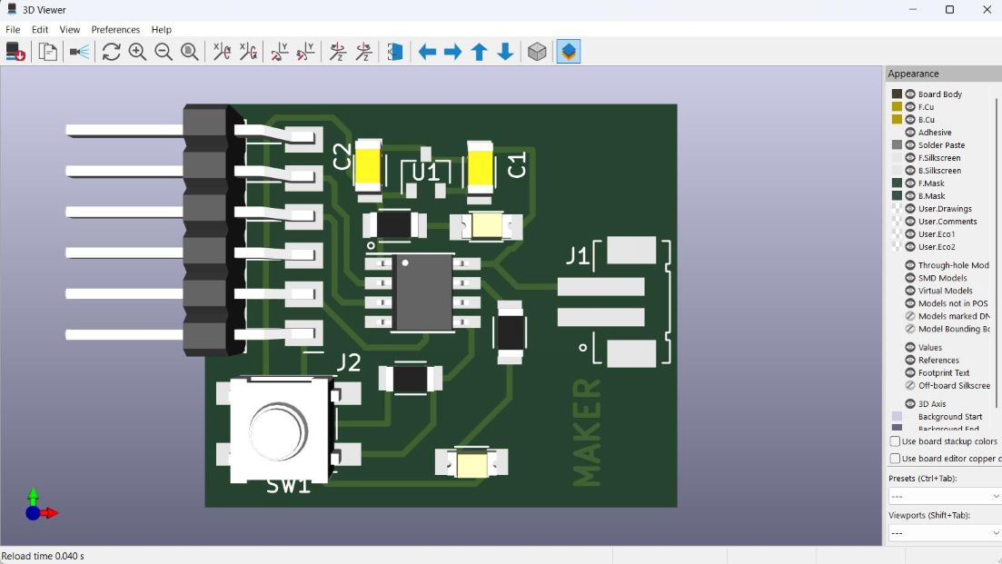
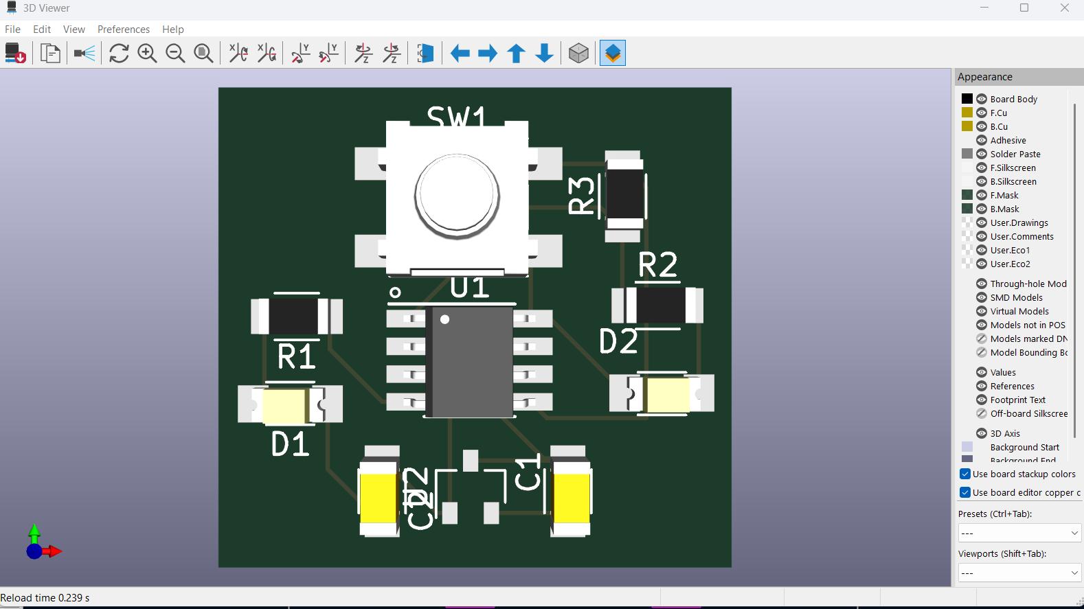
Converting in 3D Viewer
KiCad allows you to view your PCB in 3D, you can add 3D CAD files of each component individually as mentioned above or add a library of CAD Files which can be accessed by KiCad.
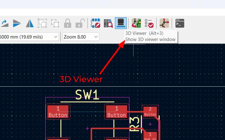
The 3D Viewer window has options for rendering, and change orientation and viewing angles for better viewing and visualization.
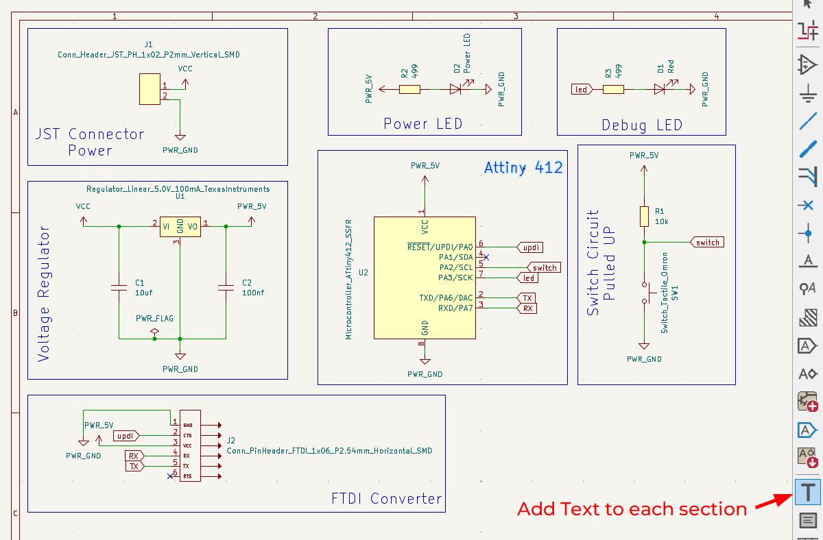
Adding more circuits and finalizing the PCB
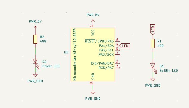
The crcuits required in the board are: Attiny 412, Voltage Regulator Circuit, Switch PULL UP Circuit, POWER LED Circuit, Debug LED Circuit, FTDI Converter(Programming Interfacing)
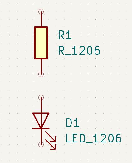
The LEDs require a resistor to limit the current. The resistors are kept in series to the LEDs. We have to decide the value of the resistor. This can be done easily using some calculations or online resistor value calculators.
I used a online resistor value calculator by DigiKey to calculate the resistance of the resistor according to the led and it's opearing voltage
LED Series Resistor Calculator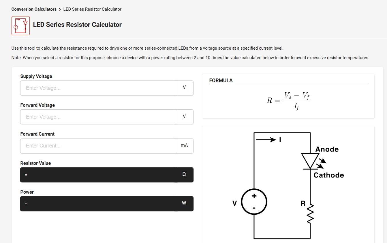
This is the datasheet available for the LEDs in the FabStash Inventory - SMD LED Datasheet
The required values of the LED are Forward Voltage and Forward Current
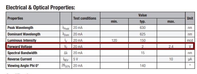
The Forward Voltage is 2.0V and Forward Current is 20mA for the Power LED. The supply voltage is 5V, therefore the resistance can be calculated using the formula: R = (Vsupply - Vled) / Iled
After calculating the resistance, the resistor value is 150 Ohm for the Power LED. But as the exact resistor was not available I used the closest bigger resistor value which was 499 Ohm
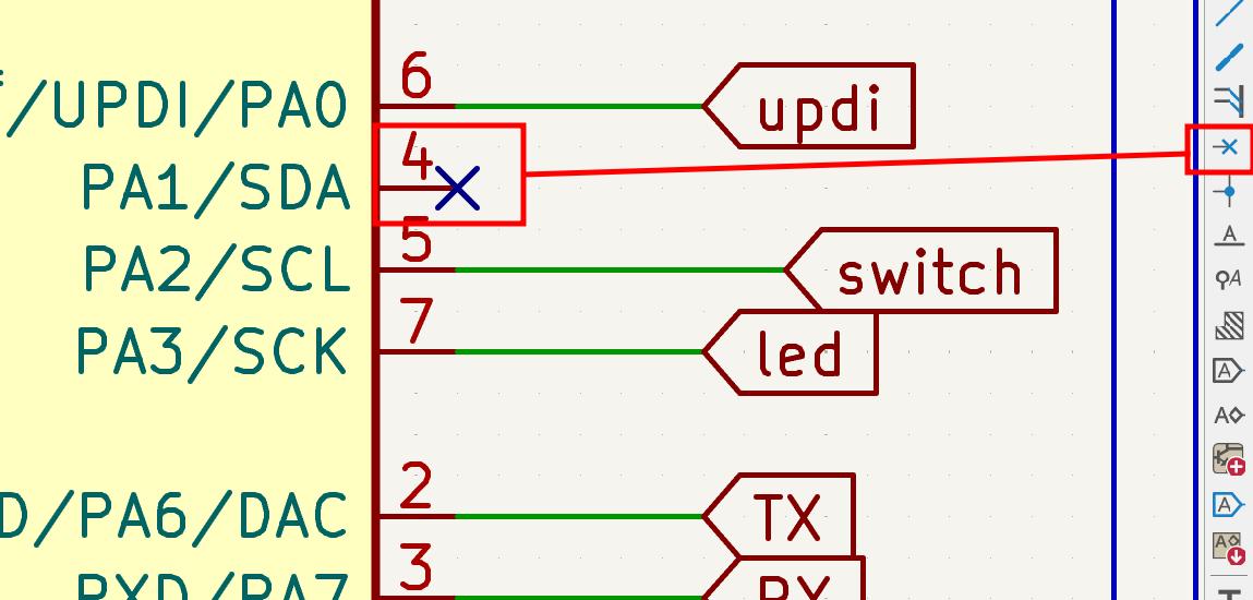
No Connect Flags
The pins that are not used must be connected as No Connect Flags
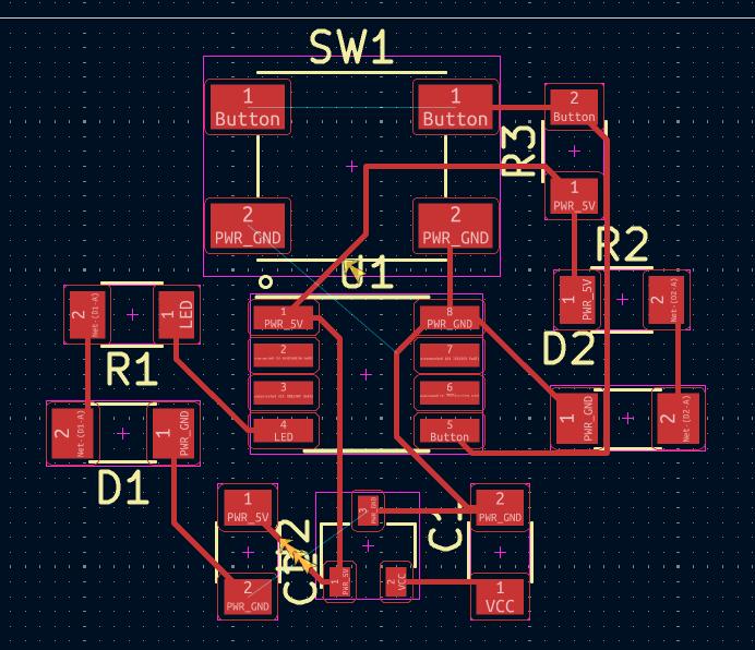
The final schematic of the demo board is below.
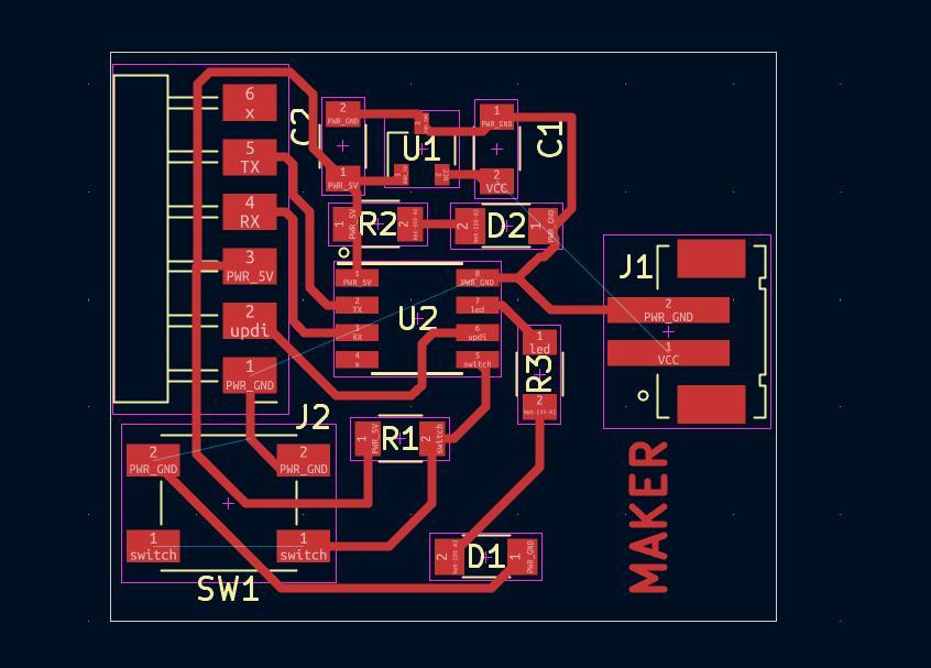
The final PCB of the demo board is below
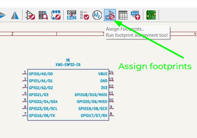
Designing Development Board using XIAO ESP32 C6
For the development board, I chose XIAO ESP32C6 as the brain of the circuit. The XIAO ESP32C6 has builtin WIFI, Bluetooth and Zigbee. it has Dual RISC-V Processors: Incorporates two 32-bit RISC-V processors, with the high-performance processor capable of running up to 160 MHz and the low-power processor up to 20 MHz.
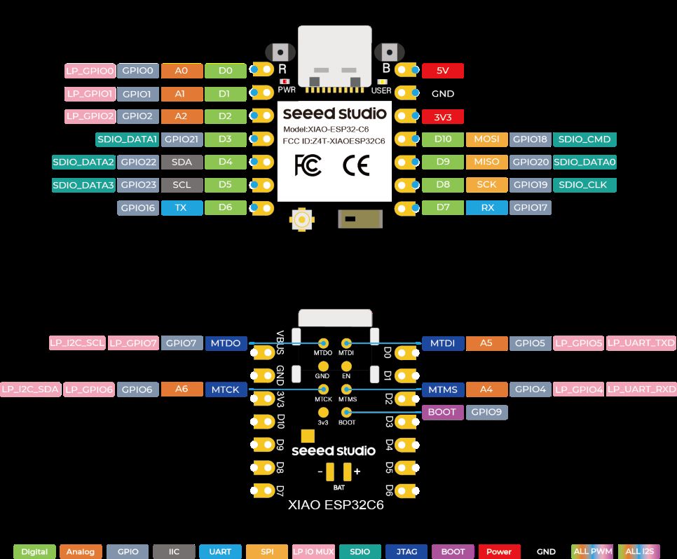
Photo credit: Openelab wiki
The XIAO ESP32C6 symbols and footprints must be added to the KiCad Project. The Fab inventory library doesn't have the specific symbol, footprint and CAD for XIAO ESP32C6. Therefore, the OPL KiCad Library can be used for this.
GitHub Repo of Seeed Studio OPL KiCad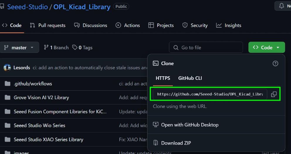
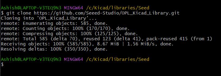
We can clone the OPL Library from the GitHub repository and add the symbol and footprint to the project. The OPL Library has a lot of components and symbols that can be used in the project. The library can be cloned using the command line or by downloading it as a zip file.


After adding the OPL Library to the KiCad Project, we can search for the XIAO ESP32C6 symbol and footprint in the library. The symbol and footprint can be added to the schematic and PCB design respectively.
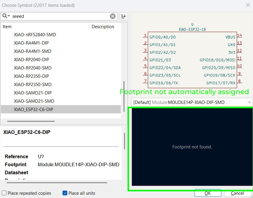
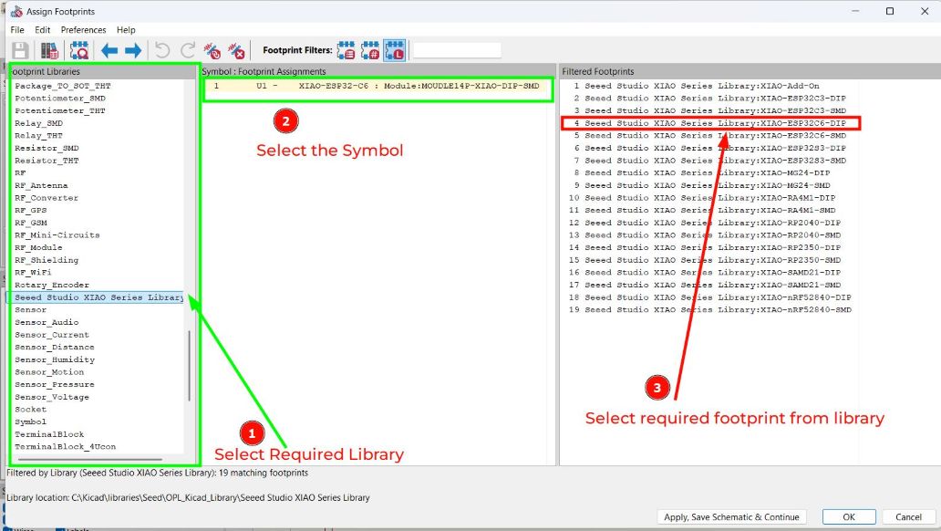
The footprint and symbol is added successfully to the project. The XIAO ESP32CS symbol and footprint is added successfully
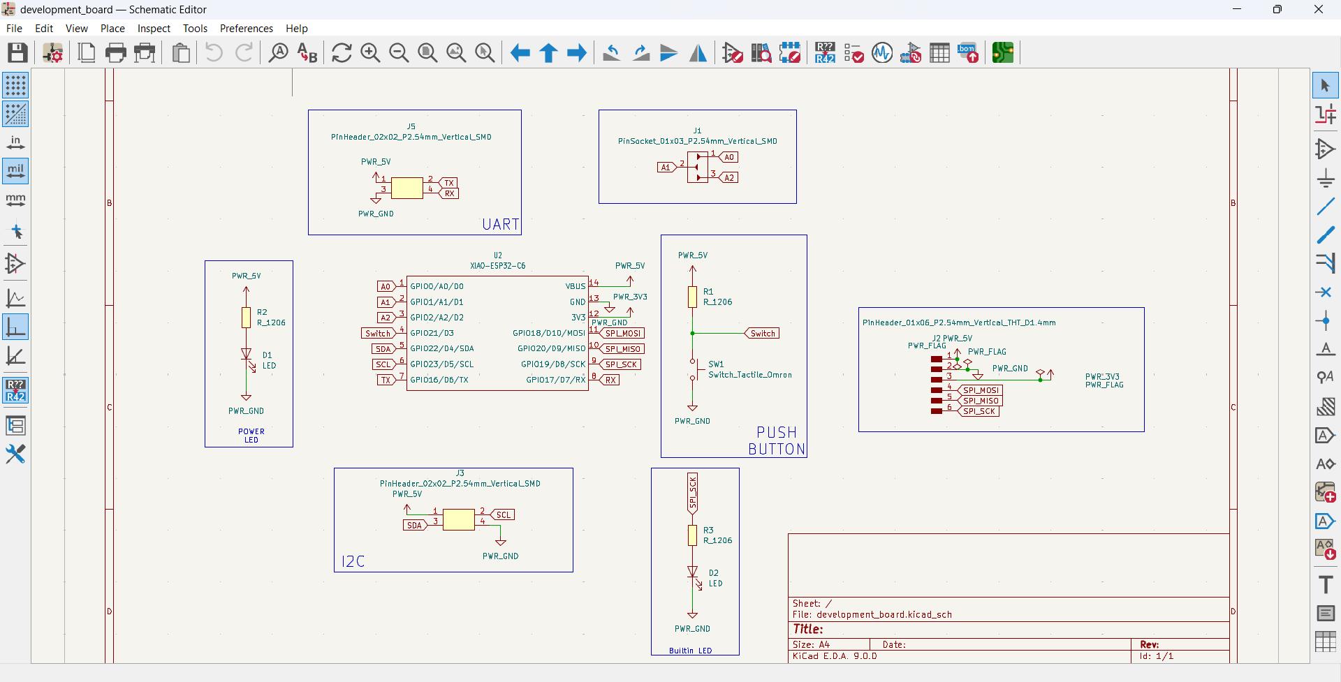
Designing the Circuit in Schematic Editor
The final schematic is made by adding the required circuits and putting the interfacing options for I2C, SPI and UART Communication.
I wanted to add a 01x06 Pin Header, but there was no symbol or footprint .So I had to make a new symbol and a new footprint. The symbol and footprint is saved as new and the footprint is assigned to the new symbol.
Editing a symbol
To edit a symbol, we can use the Symbol Editor in KiCad. We can open the Symbol Editor by clicking on the "Symbol Editor" button in the toolbar or by pressing the shortcut key 'F11'. In the Symbol Editor, we can create a new symbol or edit an existing symbol.
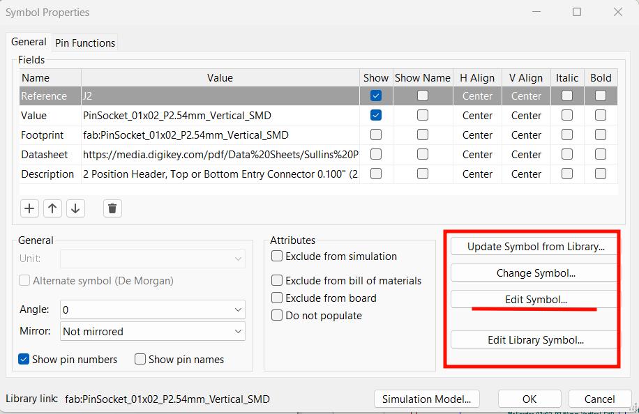
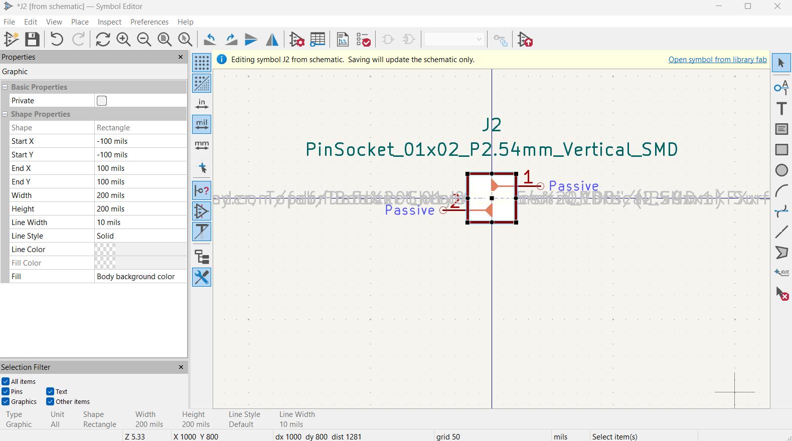
Here we edited the symbol for 01x02 Pin Header. The symbol is created by adding pins and drawing the shape of the symbol. We can also add text to the symbol to indicate its name and other information.
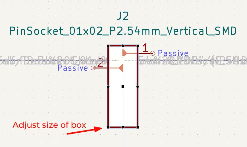
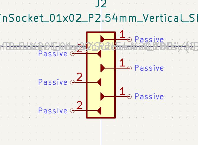
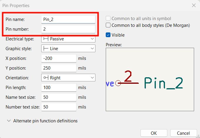
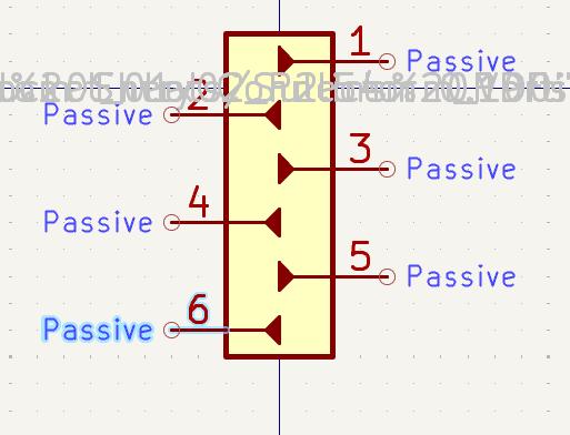
I added 4 more pins to the symbol to make it a 01x06 Pin Header. The symbol is saved as a new symbol and the footprint is assigned to the new symbol. The symbol is saved in the library and can be used in the schematic.
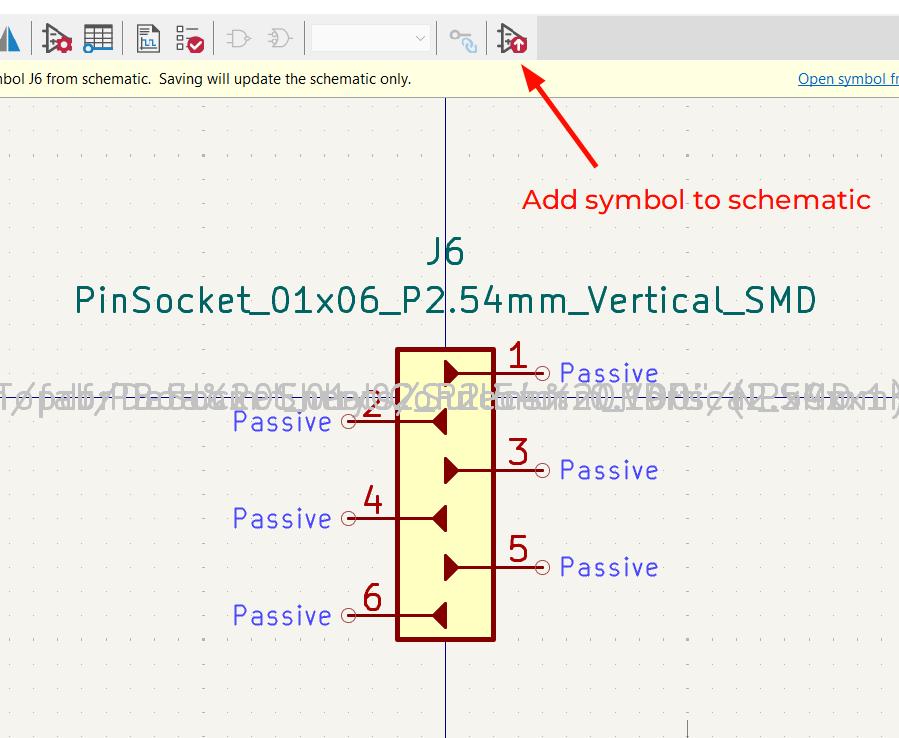
The symbol is successfully added to the schematic, now it can be used in the circuit.
Creating a Footprint
The created symbol needs a footprint, so we can edit a footprint similarly as we did for the symbol.
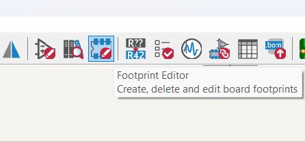
To edit a footprint, we can use the Footprint Editor in KiCad. We can open the Footprint Editor by clicking on the "Footprint Editor" button in the toolbar or by pressing the shortcut key 'F12'. In the Footprint Editor, we can create a new footprint or edit an existing footprint.
We can create a new footprint by adding pads and drawing the shape of the footprint. We can also add text to the footprint to indicate its name and other information. The pads are the areas where the components will be soldered to the PCB.
I used the PinScoket 01x02 Pin Header as a template to create the footprint. The footprint is created by adding pads and drawing the shape of the footprint. We can also add text to the footprint to indicate its name and other information.
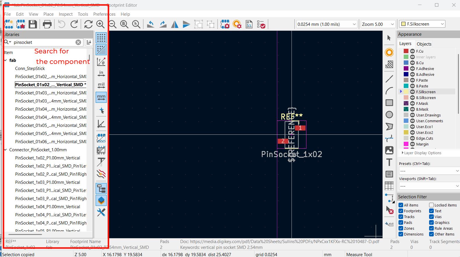
I added 4 more pads to the footprint to make it a 01x06 Pin Header.
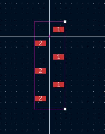
The footprint is saved as a new footprint and the symbol is assigned to the new footprint. The footprint is saved in the library and can be used in the schematic.
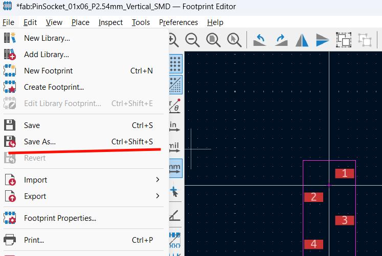
You can assign the footprint to the symbol by right clicking on the symbol and selecting the "Assign Footprint" option. This will open a window where you can select the footprint that you created.
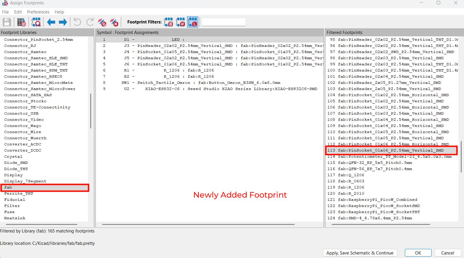
The footprint is successfully assigned to the symbol and can be used in the schematic.
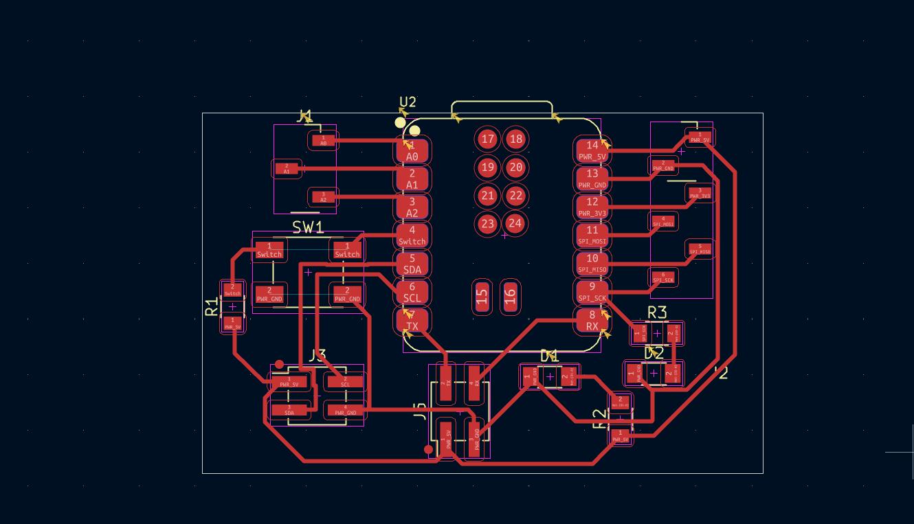
Final Board Schematic Design
The final schematic is made by adding the required circuits and putting the interfacing options for I2C, SPI and UART Communication. The schematic is designed to be used as a development board for the XIAO ESP32C6.
Final Board PCB Design
The final PCB design is made by adding the required traces and components. The PCB is designed to be used as a development board for the XIAO ESP32C6. The PCB is designed to be compatible with the XIAO ESP32C6 and can be used for various applications.
The PCB is designed to be used as a development board for the XIAO ESP32C6. The PCB is designed to be compatible with the XIAO ESP32C6 and can be used for various applications.
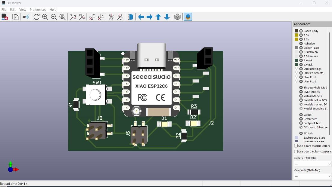
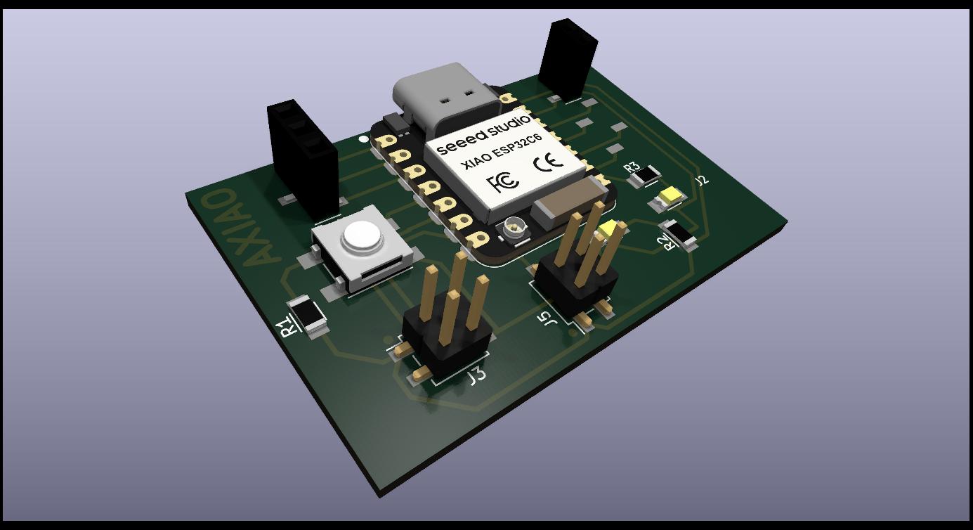
3D Viewer
The 3D Viewer is used to visualize the PCB design in 3D. The 3D Viewer allows us to see the components and traces in 3D and helps us to check the placement of the components and traces. The 3D Viewer is a useful tool for checking the design and making sure that everything is in place.
Exporting files from KiCad
YOu can export the PCB in different formats for different applications.
Exporting GERBER files
GERBER files are used for manufacturing the PCB. The GERBER files contain the information about the traces, pads, and other components on the PCB. The GERBER files can be exported from KiCad by using the "Plot" tool or by pressing the shortcut key 'F9'.
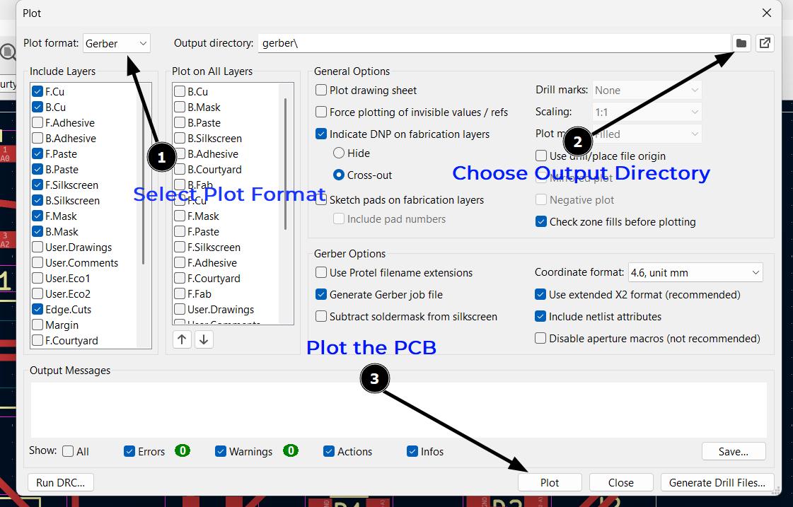
These are the steps to PLOT the gerber files
Click on the "Plot" button in the toolbar or press the shortcut key 'F9'. This will open the Plot window where you can select the layers to be plotted and the output format.
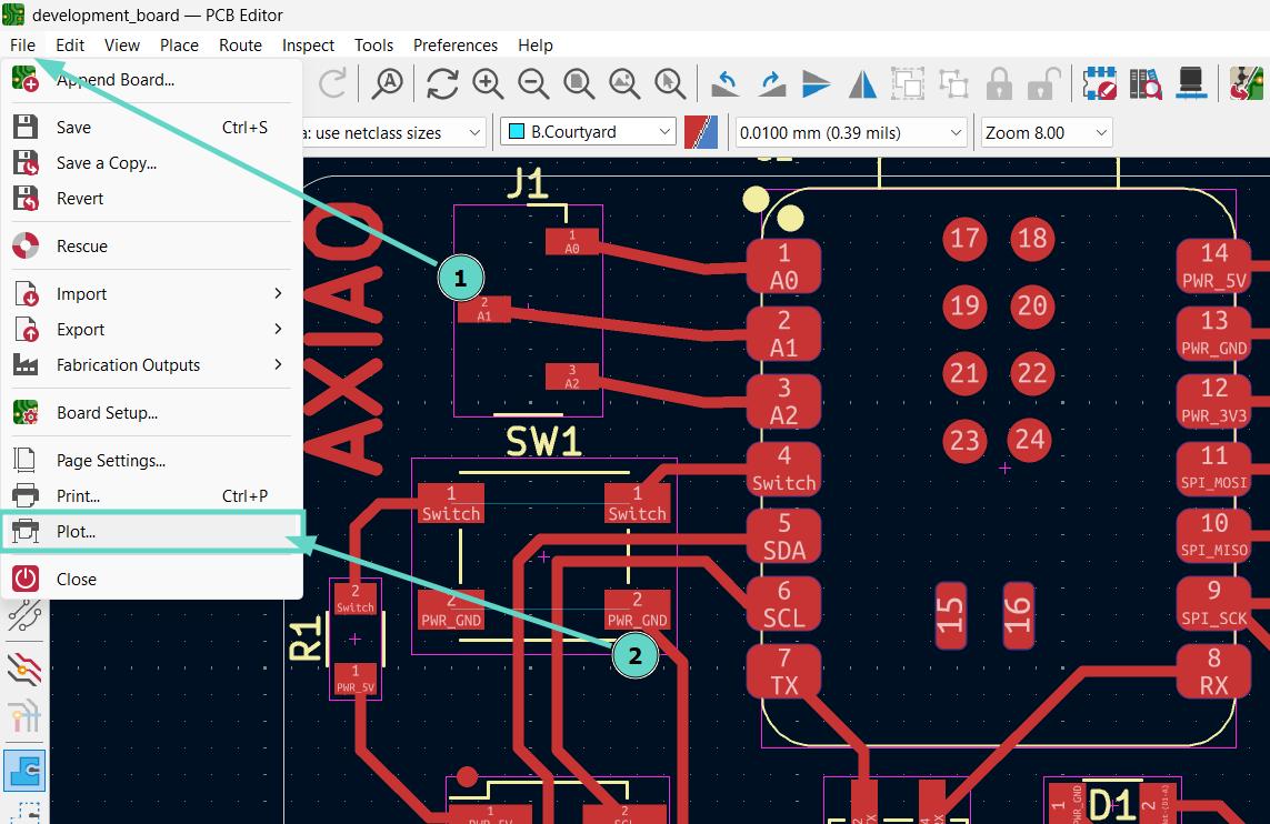
Select the format of the output files. Here we select the "Gerber" format. You can also select the output directory where the files will be saved. And click on Plot.
The output messages for a successful plot.
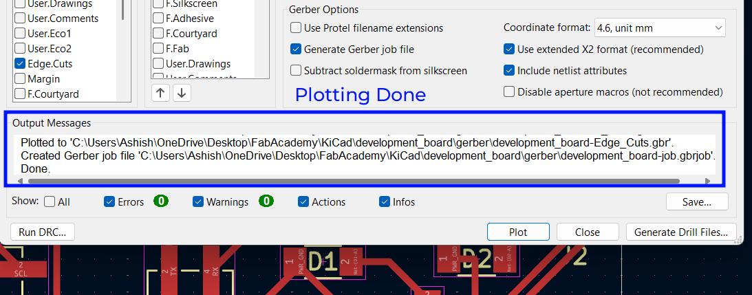
The plot files are saved in the output directory that you selected. The plot files contain the information about the traces, pads, and other components on the PCB but not the drill files. The plot files can be used for manufacturing the PCB.
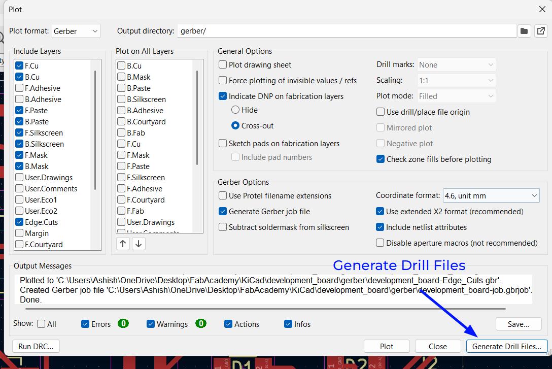
To export the drill files, we can use the "Generate Drill Files" tool. This will open the Drill File window where you can select the output format and the output directory.
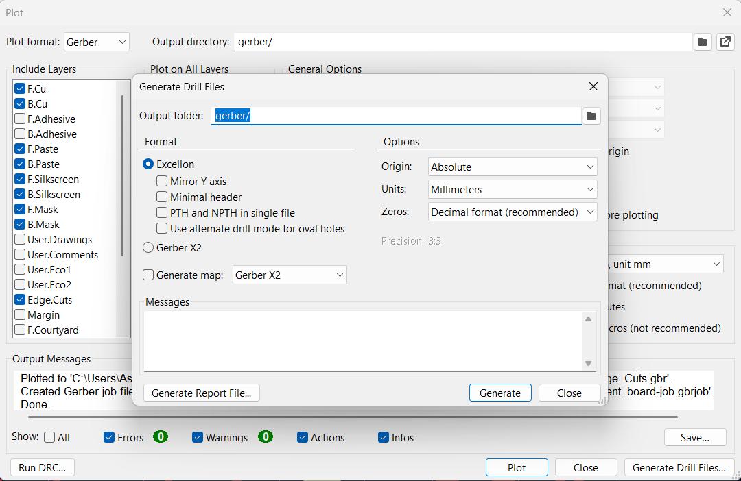
The genererated drill files contain the information about the drill holes on the PCB.
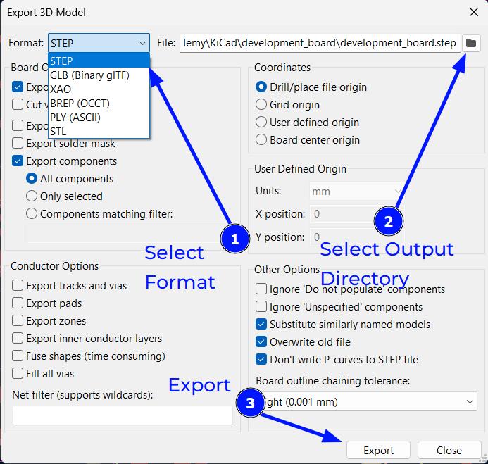
Exporting 3D File
We can export the 3D model of the PCB using the "Export Tool". There are different formats available for exporting the 3D model such as STEP, VRML, and STL. The 3D model can be used for visualization and simulation purposes.
Click on file, then on Export. This will drop down different options such as STEP, GenCAD, VRML, etc. I have selected STEP/GLB/BREP/XAO/PLY/STL...
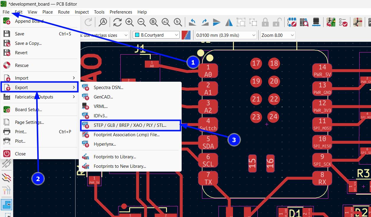
Select the format of the CAD file. I have selected STEP format and then selected the output directory and exported the STEP file.
Learnings
I familarised with the Electronic Components, Circuits and EDA which will be useful for my further assignments and projects. The design of the two PCB boards helped me to familarise with the KiCad Software and the symbols, footprints and 3D Cad files.
I would love to explore more about better placement of components,
Design Files
You can download my design files from below
Demo Board using Attiny 412
Development Board using XIAO ESP32C6
- Schematic
- PCB
- KiCad Project
- 3D Model
Trace File