Week 8
Electronics Production
individual assignment is to make and test a microcontroller development board that I have designed in the PCB design week and for extra credit make it with another process and the group assignment was to characterize the design rules for your in-house PCB production process & submit a PCB design to a board house also to make a test board using multiple processes.
Group Assignments
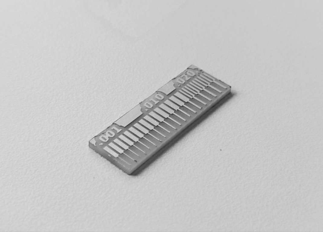
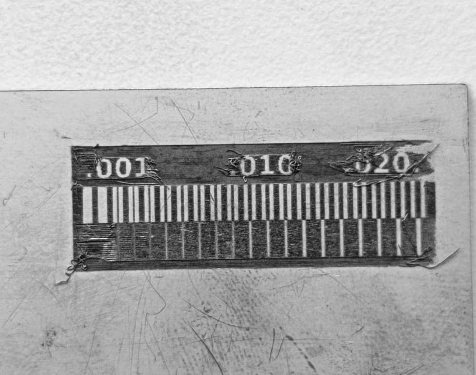
Link : week 8 Group Assignment
For this week we were supposed to characterize the design rules for our in-house PCB production process and submit a PCB design to a board house and also make a test board using multiple processes like X Tools laser Engraver, Trotech laser engraver, Solder mask & Flexible PCB.1/64” Flat End Mill All test widths .015 inch Wider isolation channels with clean, straight edges. Material removal is more substantial compared to V-bits. V-bit 0.2mm All test widths .010 inch Moderate isolation channel width. Good balance between precision and durability. V-bit 0.1mm All test widths .005 inch Finest isolation channels with minimal copper removal. Excellent for high-density designs.
PCB MILLING
PCB milling is a process of creating printed circuit boards (PCBs) using a CNC (Computer Numerical Control) milling machine instead of traditional chemical etching. The milling machine removes copper from a laminated board to create electrical pathways, leaving behind the necessary conductive traces, pads, and other features.
This is the setup we have in our lab and we have a beautiful view out of the window
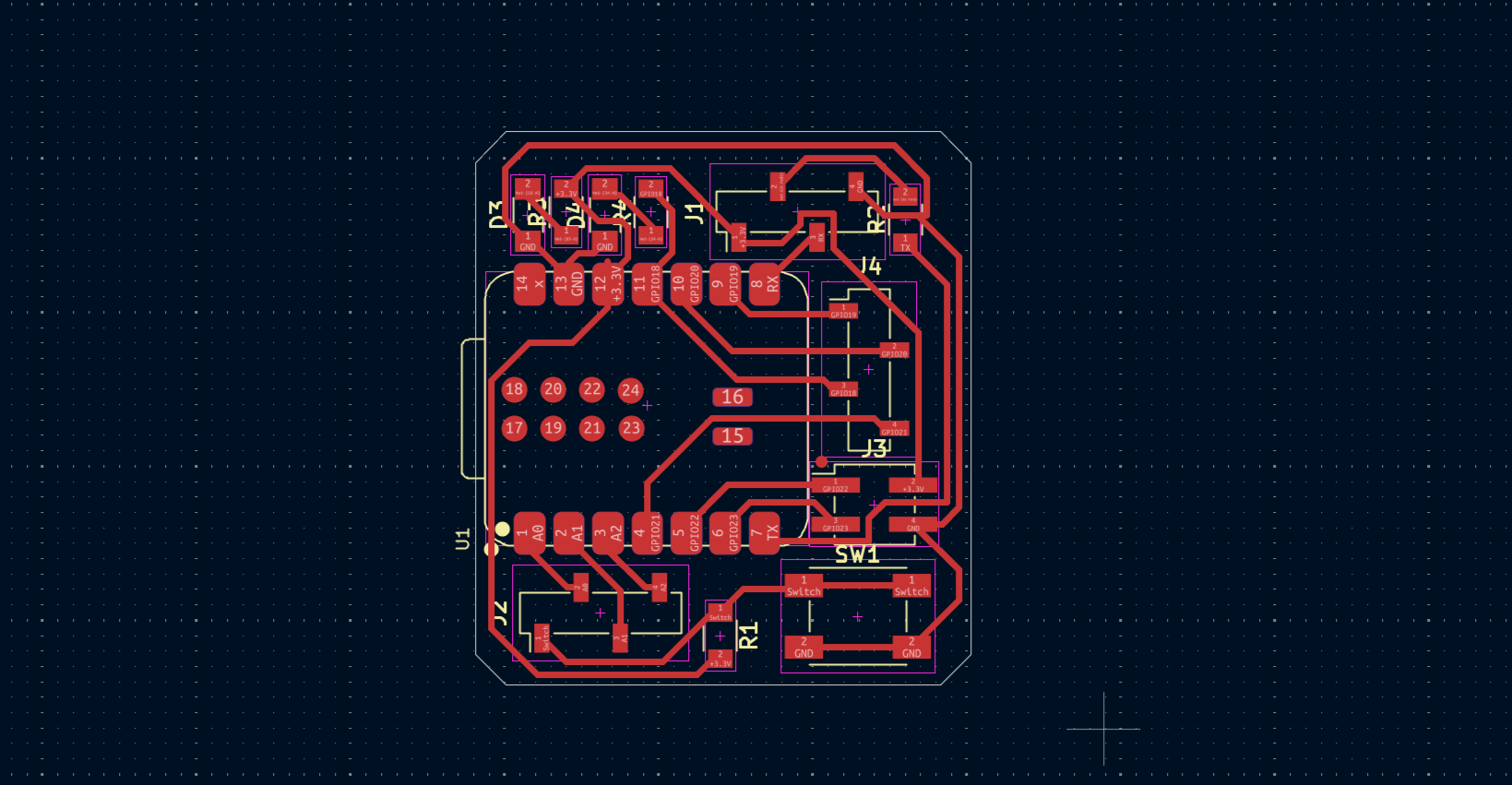
This week I am going to mill the pcb that I created in the PCB design week.
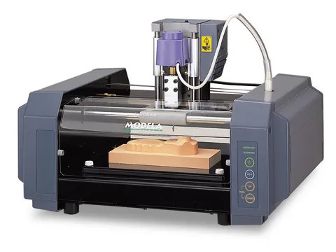
Modela MDX-20 3D Milling Machine
The **Modela MDX-20** by Roland DG is a compact, desktop 3D milling machine designed for prototyping, light production, and education. It mills materials like wax, foam, wood, acrylic, and soft metals with high precision. Key features include automatic tool sensing, a user-friendly interface, and compatibility with software like SRP Player for creating toolpaths from 3D models.
a work area of 203.2 mm x 152.4 mm x 60.5 mm and a spindle speed of 6,500 RPM, it’s ideal for detailed projects such as product prototyping, mold making, jewelry design, and architectural modeling. Its compact size and ease of use make it popular in schools, small businesses, and labs. The MDX-20 is a versatile tool for bringing 3D designs to life with accuracy and efficiency.
Website : www.rolanddga.com
Milling tool
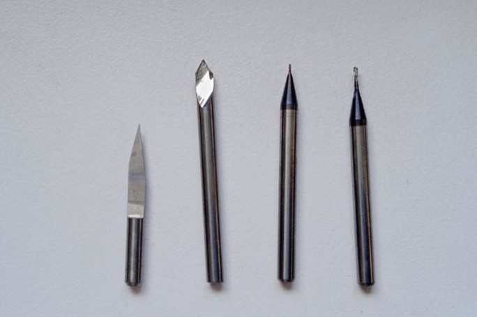
These are the tools available her 2 V bits and 2 flat end mills1 one of the flat end 1/32" and the other one is 1/64" bit the bigger one is generally used for large surface clearing or for drilling
Setup
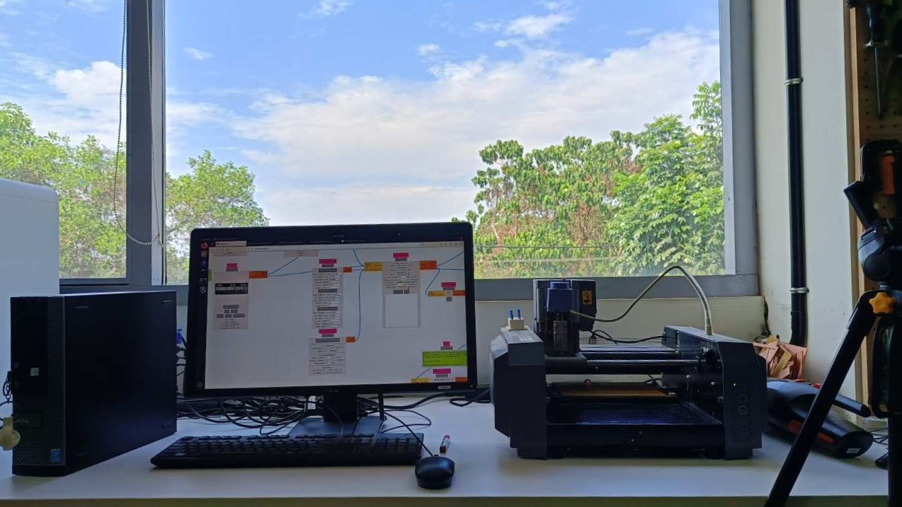
Milling My PCB
we were given a board to mill first i inspected the boar for any issues through visual inspection.
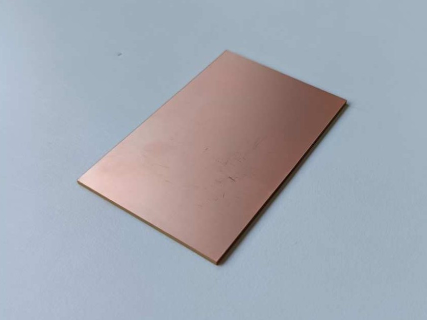
The next step was to apply adhesive layer o the bottom part of the board.Then i loaded the board into the milling machine and set the origin of the board.
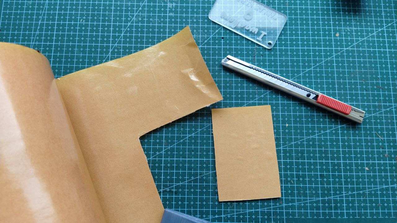
While loading the board on to the milling machine, I made sure to align the board properly as much as possible
Fist step was to export the gerber file from the KiCad and convert this into a PNG File, For this I used the Gerber to PNG converter tool from the Super fab lab kochi
Link : https://gerber2png.fablabkerala.in/
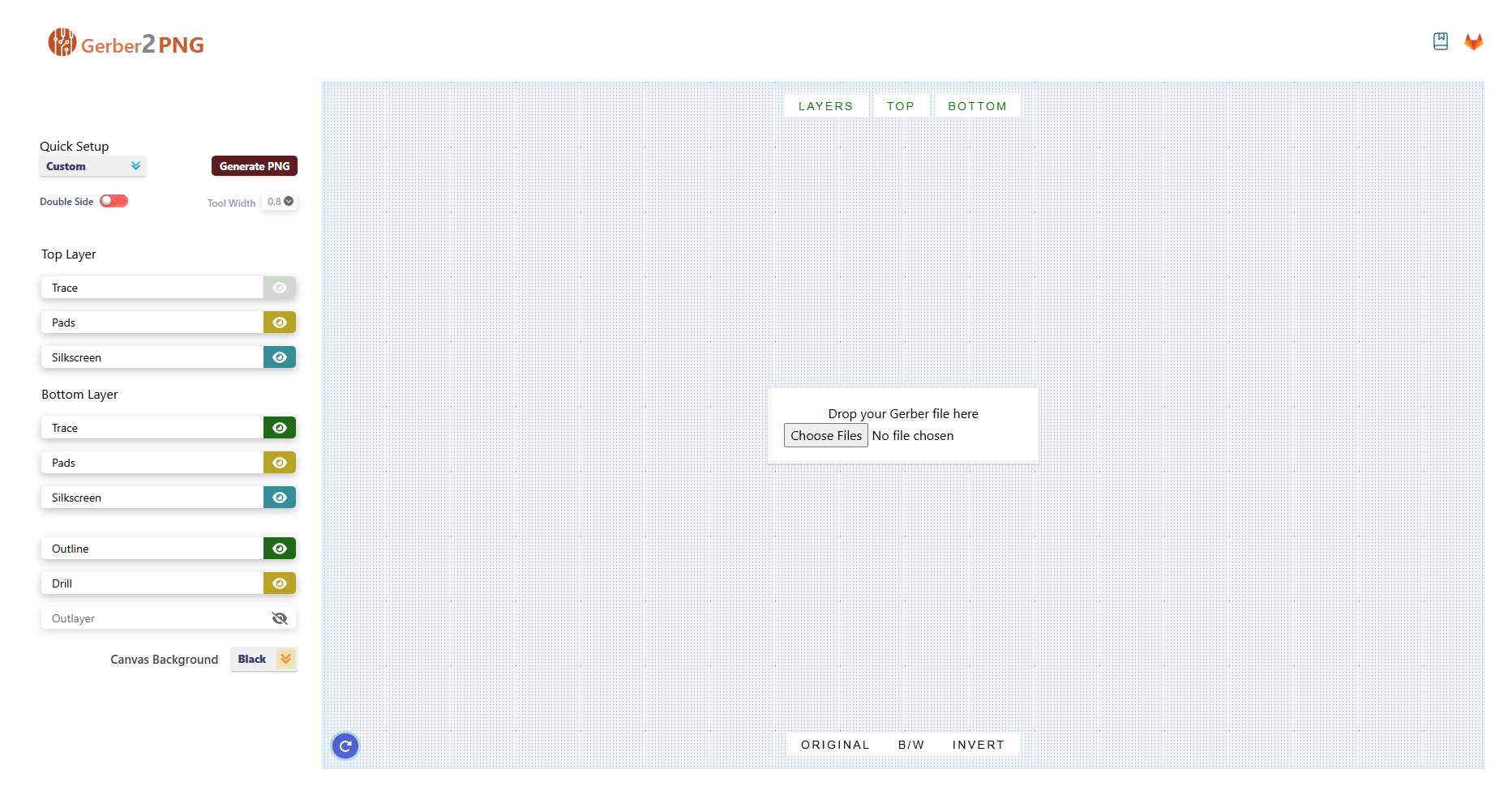
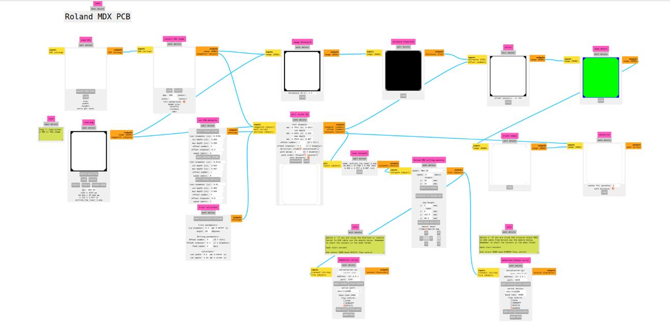
The next step was to set up the Fab mods for the milling machine, first open fab mods then open the mod setup for the specific machine.
In this case I have two kinder of process one is milling and second is cutting. Then first I took the PNG file and loaded it into the mods and then selected the tool for milling I am using the v tool
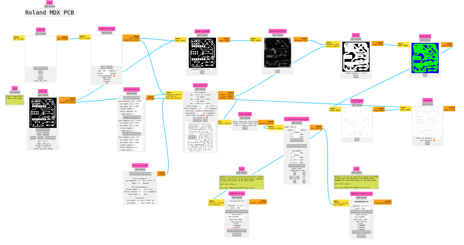
Milling Tracks
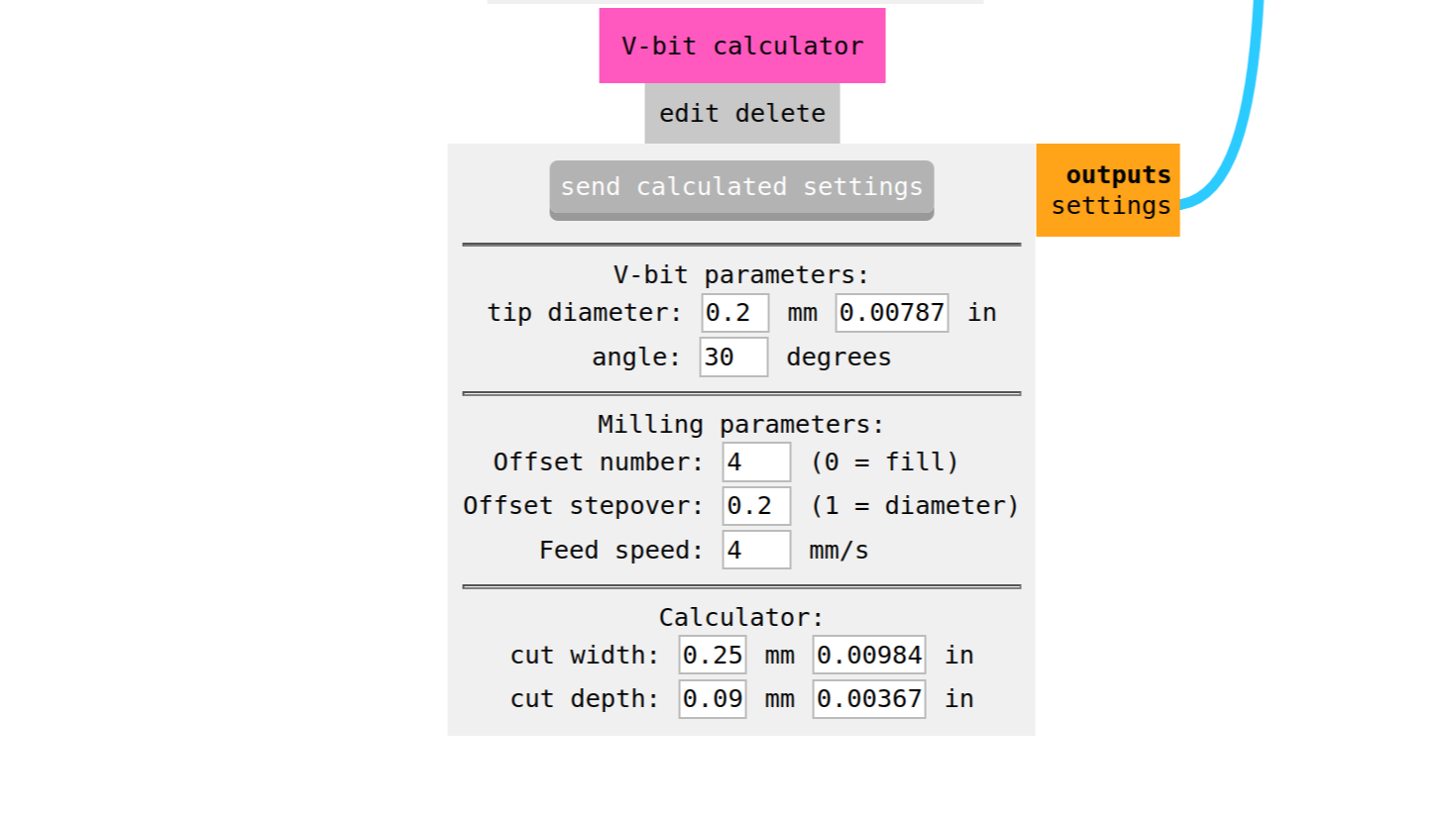
Then I set the values of the V tool and then send the calculated setting and after that calculated ever thing was looking good
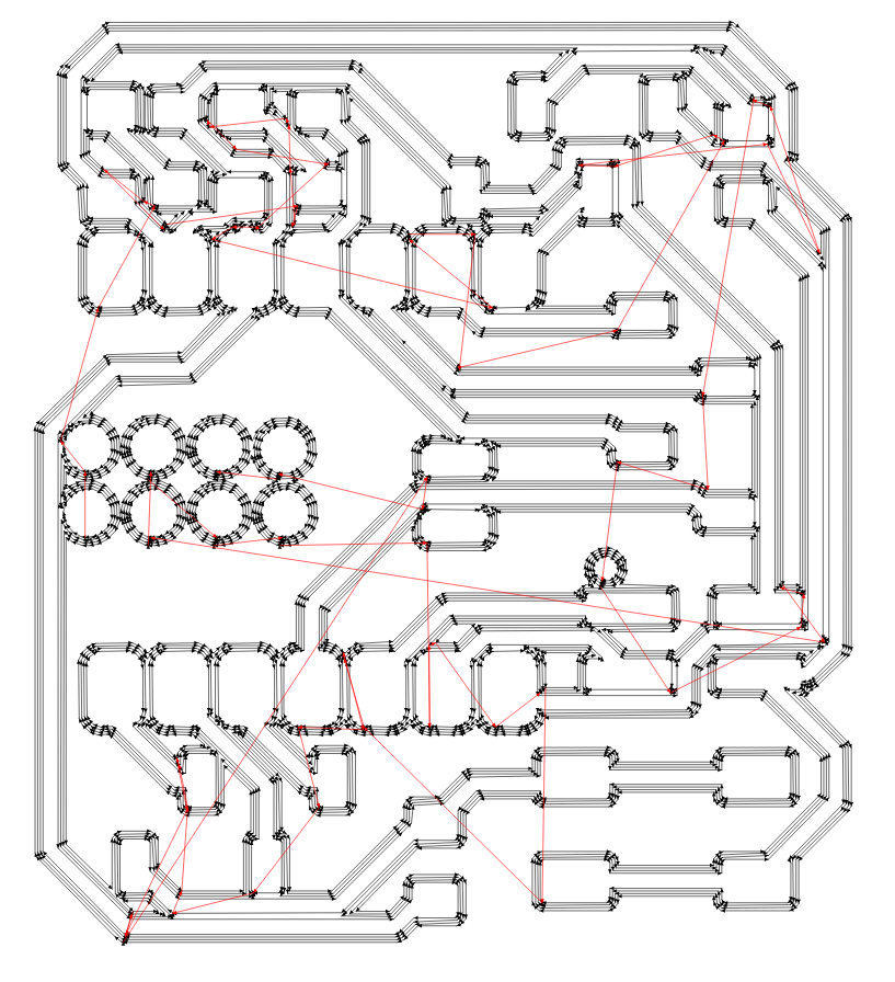
Then I checked the path of milling to make sure that the milling wall be done properly.
NOTE : The value we gave for the angle of the tool bit was 30deg but actually it was 60deg this error may have lead to the issue of not removing the copper properly that i faced while milling.
And for changing the tools our instructor had added a custom button for this position to change bit after pressing the the machine will go into a position where it is easy to change the bit.
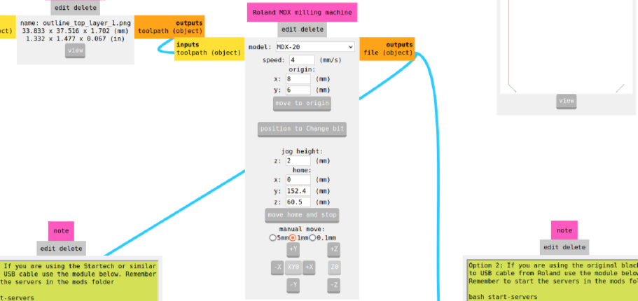
After completing the set up the next step was to load the tool needed for milling, This first step should be always milling the copper layer for this I loaded the v tool using the allen key first from the mods press the tool change button then loaded the tool make sure the tool is inserted into the milling machine so that only the fluts of the tool is visible are then moved the tool to the origin.
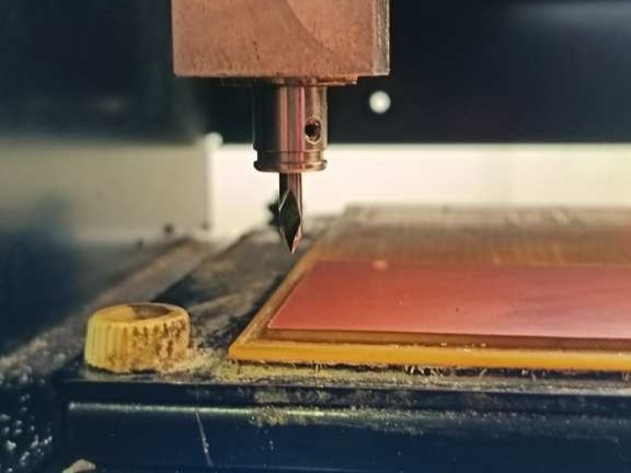
Now when to tool reaches the origin move the Z axis down using the button on the milling machine and when there is almost 10 mm from the milling surface stop and loosen the tool and adjust the height and make sure that the tool make proper contact with the board and then properly tighten the tool. And then start milling
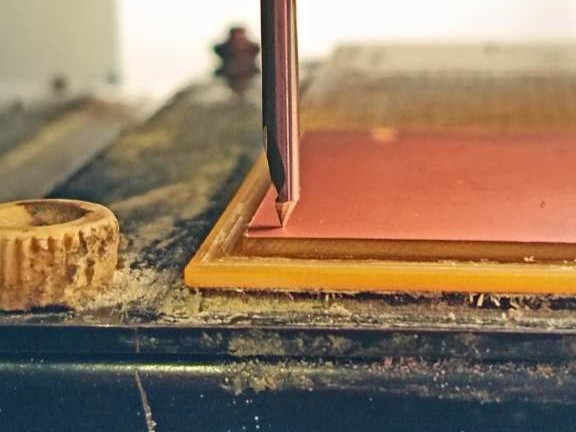
After setting the the origin we can easily move the tool in X or Y axis since the tool hops from point a to point b & an fount it very interesting and it looks good.
After this I started milling but the toll was properly removing the coper layer from the board even thought the depth of cut was set .1 mm the material was not being removed properly.
So to solve this issue I brought the tool to the origin and loosen the tool and made the tool properly come in contact with the board and then tightened the tool. and started the milling.
After the milling was done I inspected to board to make sure that the milling had been done properly
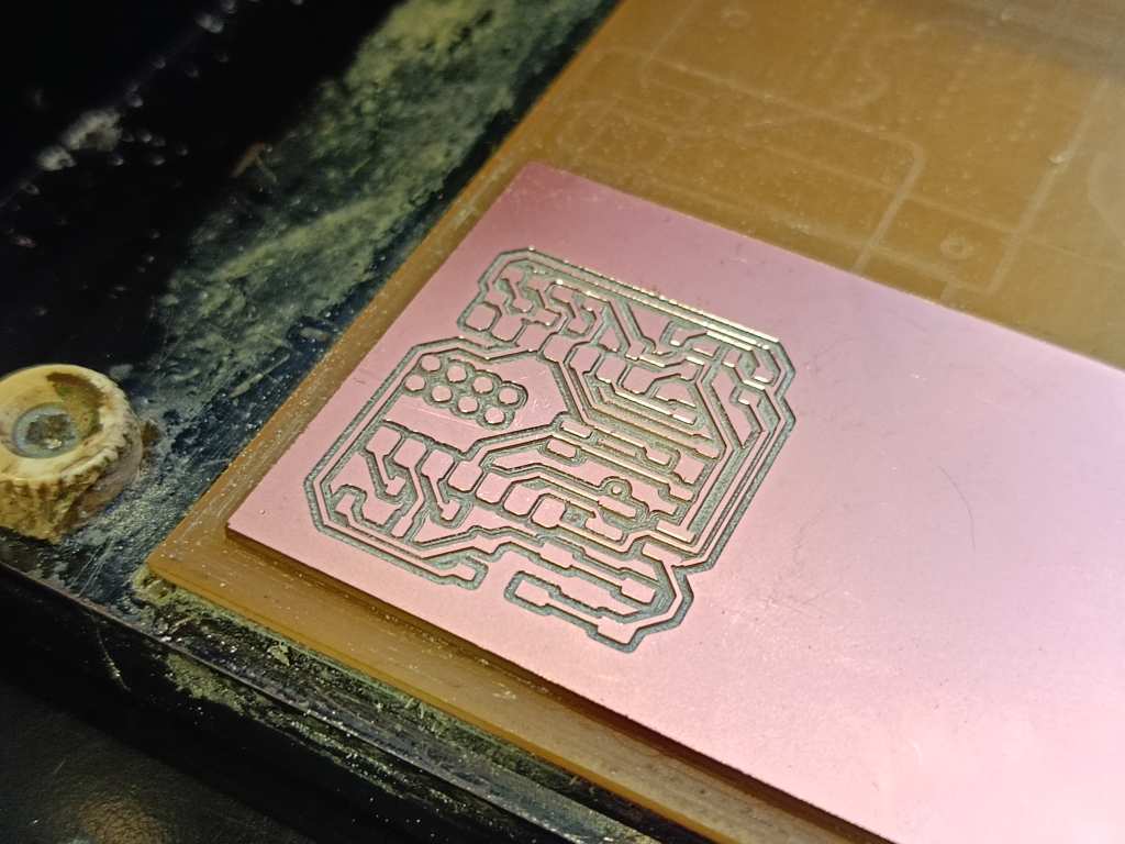
Cutting
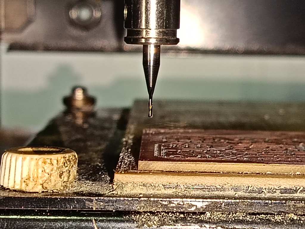
Then next step was to start cutting for this I changed the tool that we are going to use in fab mods. Since we are using the .8mm cutting tool a selected the tool from the interface.
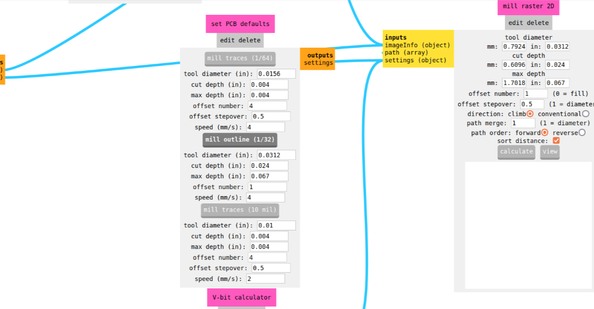
After doing this I proceed to import the PNG file for making the cut then I proceeded with calculation after this I moved to the machine.
Now the next step was to cut so I loaded the .8mm cutting tool
And them repeated the same process done for the v tool and made sure the tool is making proper contact with the board.
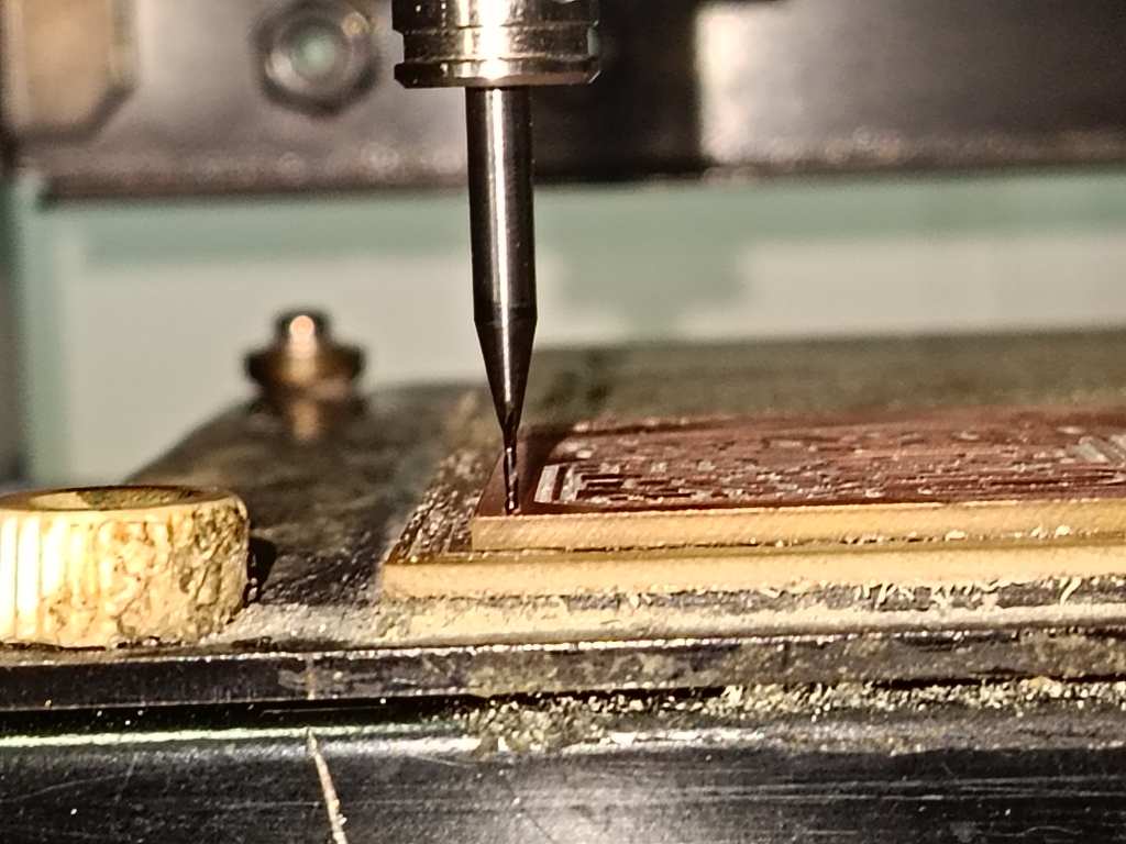
Then I proceeded with cutting this time there were no issues the cutting was done properly.
After the cutting was done I cleaned the workpiece and inspected the board to make sure that the milling and the cutting had been done properly and it was good.
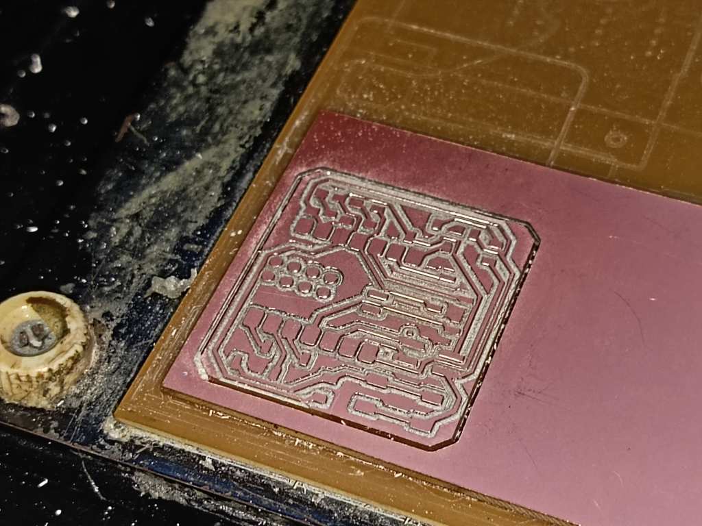
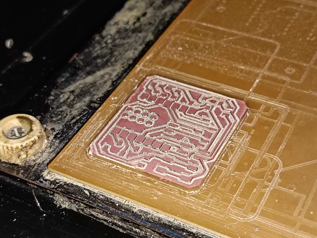
After this I first removed the part where the board was not supposed to be cut and then I removed the milled material and cleaned the board
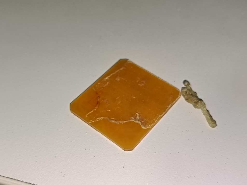
I also made sure to remove all the adhesive from the bottom of the board.
After this I made sure that the board properly fits inside the encloser that was designed and 3D printed in the PCB design week.
How to Add Fuzzy Texture in Bambu Studio
- Open Bambu Studio and load your 3D model.
- Select the model in the left panel.
- Go to the "Object Settings" tab (gear icon on the right).
- Scroll down to find the "Surface Mode" section.
-
Enable "Fuzzy Skin":
- Check the box for Enable Fuzzy Skin.
- You may need to click Advanced if it's hidden.
-
Adjust parameters (optional):
- Fuzzy Skin Thickness: How far texture sticks out.
- Fuzzy Skin Point Distance: Controls roughness/detail.
- Fuzzy Skin Pattern Angle: Changes fuzz direction.
- Click Slice and preview the layers to check the texture.
- Export the G-code and send it to your printer.
Soldering
Soldering is the process of joining two or more electronic components by melting solder around the connection. This creates a strong electrical bond. It typically involves a heated soldering iron, solder wire (usually made of tin and lead or lead-free alloys), and careful handling to avoid damaging components or creating short circuits.
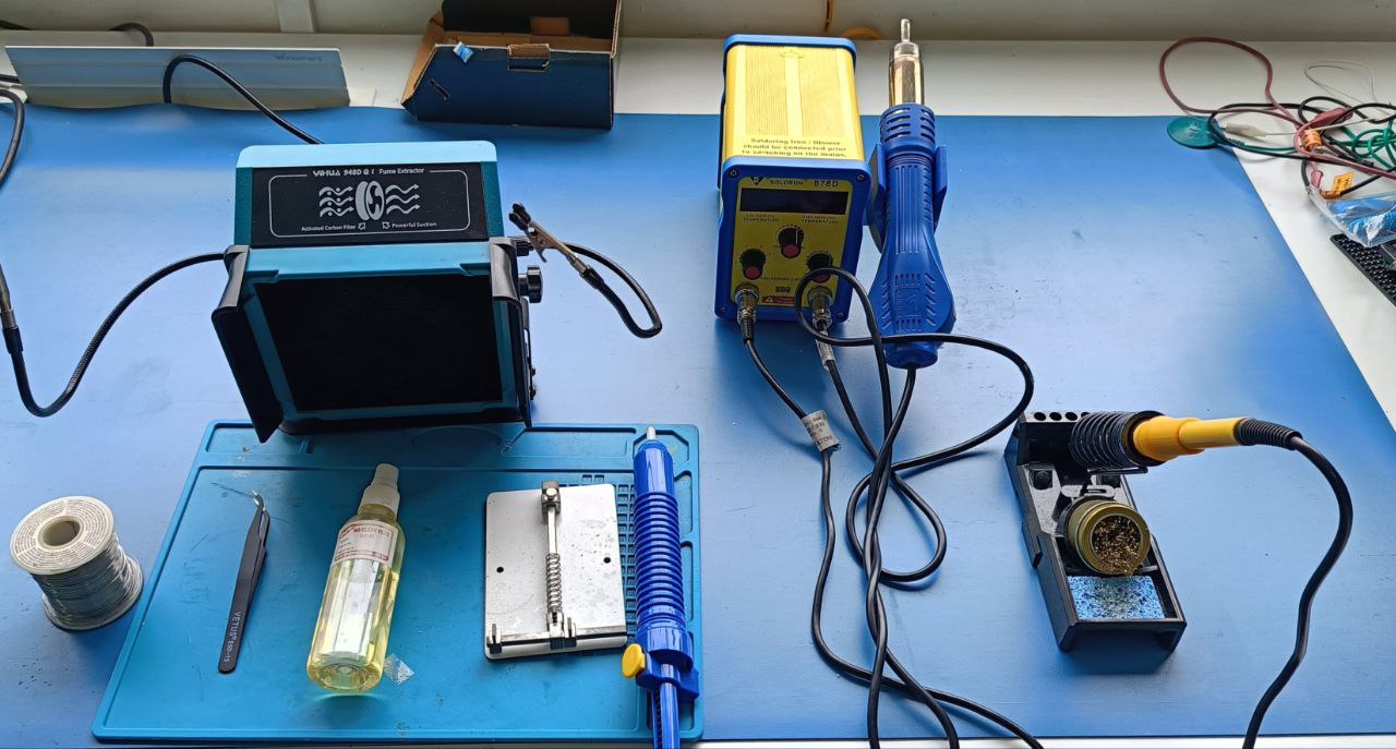
1. Soldering Wire: This is a thin metal wire that melts when heated and is used to join electronic components to a PCB. It typically contains a core of flux to help with the soldering process.
2. Tweezers for Soldering: Precision tweezers are used to hold and place small components during soldering. They help position parts accurately and keep fingers safe from the hot tip of the soldering iron.
3. Liquid Soldering Flux: This chemical solution is applied to PCB pads and component leads before soldering. It removes oxidation, improves solder flow, and ensures strong, clean joints.
4. PCB Holder: A PCB holder or vise secures the circuit board in place while soldering, making the process easier and more accurate by preventing movement.
5. Soldering Pump: Also known as a desoldering pump, it is used to remove molten solder from joints. It’s essential for correcting soldering mistakes and removing components.
6. Soldering Mat: A heat-resistant silicone mat used to protect the work surface from heat and solder spills. It often has compartments to hold tools and components.
7. Soldering Iron: A handheld tool with a heated metal tip used to melt solder wire. It is the primary tool for creating solder joints between components and PCBs.
8. Heat Gun: A tool that blows hot air and is used for soldering or desoldering surface-mount components, as well as for heat shrinking tubing and other heating tasks.
9. Power Supply with Temperature and Fan Speed Control: This unit controls the temperature of the soldering iron and heat gun, and regulates the airflow speed of the heat gun fan, allowing precise control for different soldering tasks.
10. Exhaust Fan: Used to remove harmful fumes generated during soldering. It improves air quality and ensures a safer working environment.
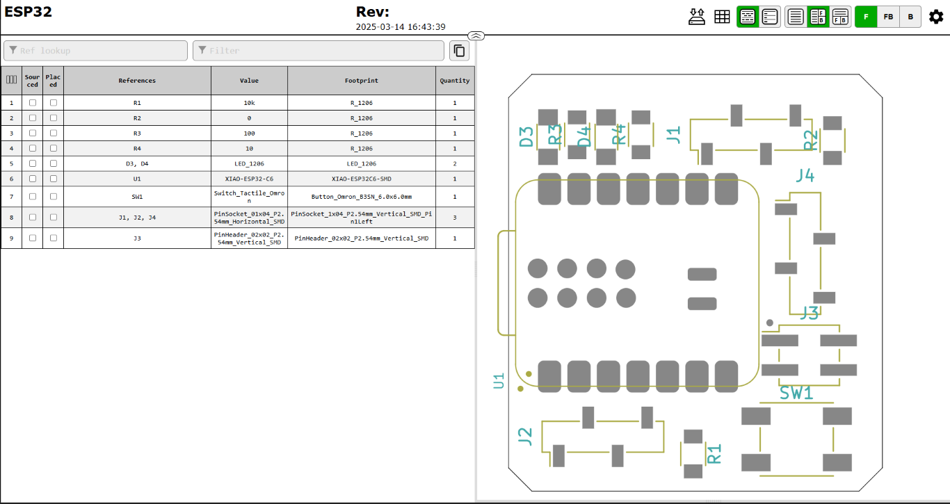
The fist step before soldering was to collect all the component needed for soldering from the inventory.For this first I exported the BOM from the KiCad .For this and for making the assembly process easier i installed the Generate Interactive HTML BOM plugin from the KiCad extensions.
The next step was to request for all the components needed for soldering through Fab stash which is an online inventory management website from super fablab kochi.
Link : inventory.fablabkerala.in
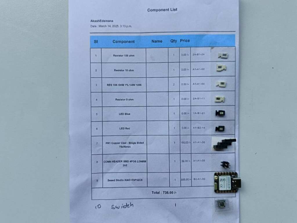
From fab stash I added al the comports needed to art and requested it & then took a printout and applied double side tape to it.Then collected all components from inventory and arranged then on the printout for easier assembling.
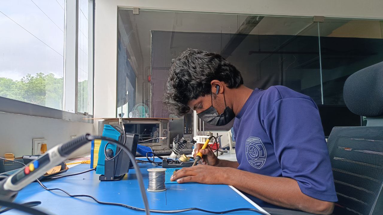
The next step was to solder the components to the board for this first I cleaned the board then placed the components on the boar.I soldered the components one by one and then soldered them.Also I made sure to start from the smaller components and solder them first.
Soldering Process
1. Prepare the Workspace: Set up your soldering tools on a clean, heat-resistant surface. Ensure you have good ventilation or an exhaust fan running.
2. Clean the Components: Make sure the PCB pads and component leads are clean and free from oxidation. You can use isopropyl alcohol or apply a small amount of flux.
3. Place the Component: Insert the component leads through the correct holes in the PCB or position the surface-mount component using tweezers.
4. Heat the Joint: Touch the soldering iron tip to both the component lead and the PCB pad. Let them heat for a second or two.
5. Apply Solder: Feed solder wire into the heated joint, not directly onto the iron. The solder should flow around the pad and lead, forming a shiny, cone-shaped joint.
6. Remove the Iron: Once the joint is fully soldered, remove the solder wire, then the iron. Let the joint cool naturally.
7. Trim Excess Leads: If using through-hole components, cut off the extra lead lengths using wire cutters.
8. Inspect the Joint: Check for cold solder joints, bridges, or incomplete connections. A good joint should be shiny and solid.
9. Clean the Board: Use isopropyl alcohol and a brush to remove leftover flux residue for a neat and professional finish.
But here I had made multiple mistakes as pointed out in the image,since the board pretty small there were some pills on the board and the major mistake that I made was due to misunderstanding I thought i was supposed to fully cover the top of part of the pad s on the micro controller and after solder i was filling those regions separately but my instructor pointed out it was not the correct way to solder, rest everything was looking good.
.png)
After this i tried assembling the board In the Encloser that I had made and tested if ever thing was filling properly and it was good the switch was working and all the ports were accessible and everthing was fitting properly.
Testing and programming
The next step was to test the board for this I first connected the board to the computer and checked if the board was being detected by the computer and it was being detected. At the same time I also tested if the power LED was working properly.
then made a schematic of the board that can be referred for programming the board.
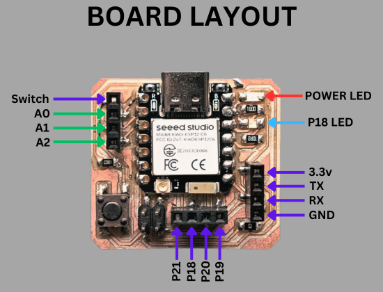
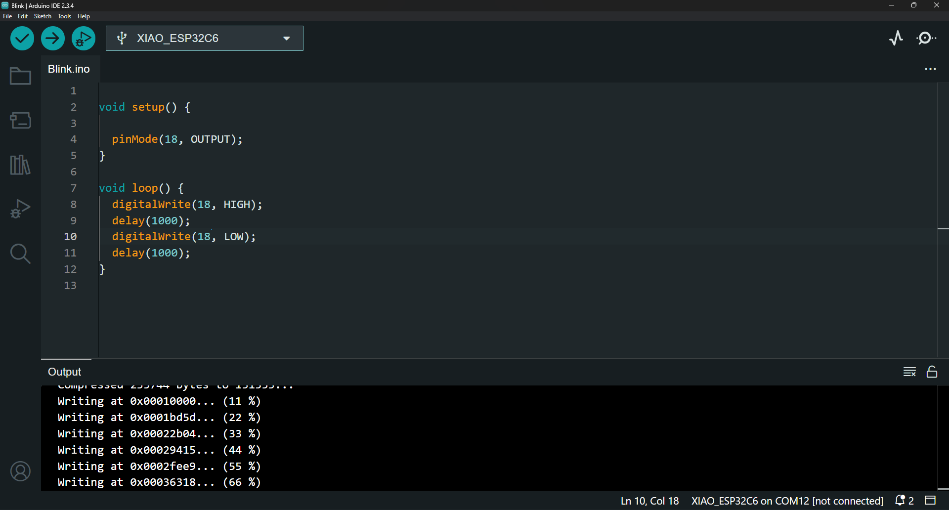
The next step was to program the board for this I used Arduino IDE and then installed the necessary libraries and then connected the board to the computer and then selected the board and the port and then uploaded the code to the board and the code was uploaded successfully.This code was was to test the external LED for this I connected the external GPIO Pin 18 and then uploaded the code to the board and the external LED was working properly.
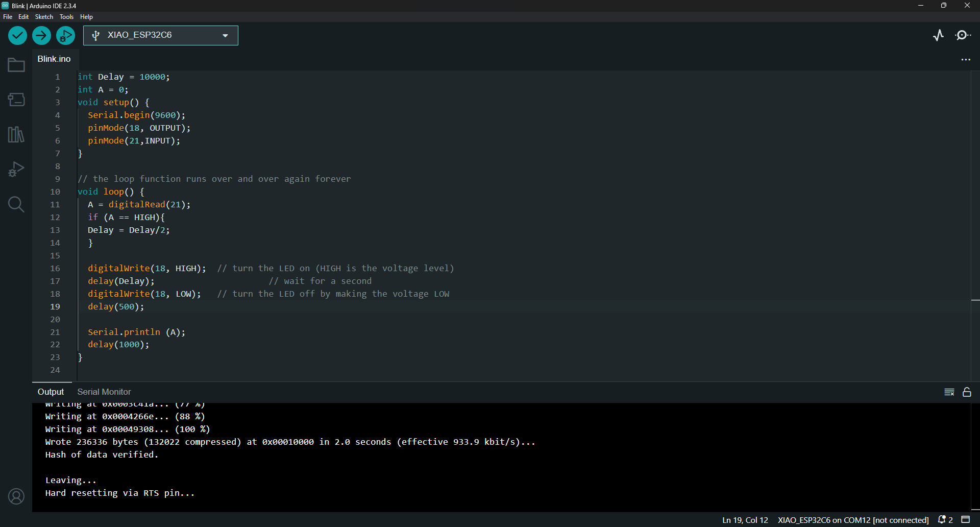
Next I tried programming with the switch here I tested the switch, In my board there is a sported output for the switch which can be connected to any GPIO pin.so I connected the switch output to GPIO pin 21 and then uploaded the code to the board and the switch was working properly.this grogram reduces the blink delay of the LED for each press of the switch.
Conclusion
For this week I have successfully made my custom PCB, For this I milled the track using a milling machine then I soldered the components on to the custom made board and tested if the board is working properly and I have also explored all the safety that has to be followed while soldering and milling and also learned to usee the basic devices for soldering and testing.

