Week 6
Electronics Design
This week's assignment focuses on both group and individual tasks related to microcontroller circuits and development board design. For the group assignment, we will use the test equipment available in our lab to observe the operation of a microcontroller circuit board. Individually, we will use an EDA tool to design a development board that incorporates components from the inventory to interact and communicate with an embedded microcontroller. Additionally, for extra credit, we have the option to design a case around our development board.
Group Assignments
We learned the basics of electronics
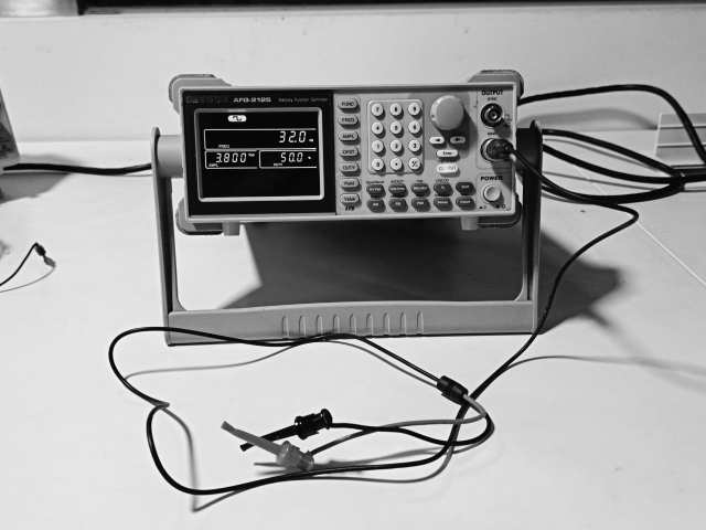
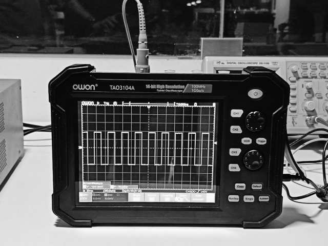
In this group assignment, we explored the operation of a microcontroller circuit board using various test equipment in our lab. We utilized a multimeter to measure voltage, current, and resistance, ensuring proper circuit functionality. An oscilloscope helped us visualize and analyze electrical waveforms, while a function generator provided test signals to simulate different input conditions. The bench power supply allowed us to power the circuit with stable voltage and current control, and the logic analyzer enabled us to capture and debug digital signals. Through this hands-on exploration, we gained valuable practical experience in troubleshooting and analyzing microcontroller-based systems.
Link : week 6 Group Assignment
Basic components
Component |
Description |
|---|---|
| Ribbon Cable | A flat cable with multiple parallel wires, used to connect internal components in electronics. They can be used for data transfer or power distribution. |
| IDC Connector (Insulation Displacement Connector) | A type of connector that pierces the insulation of a ribbon cable to make electrical contact. These are commonly used in ribbon cables for quick and reliable connections. |
| Button | A simple switch that completes or breaks a circuit when pressed. |
| Switch | A device that opens or closes a circuit to control the flow of electricity. Can be manual (like a light switch) or automatic (like a relay). |
| Resistor | A component that limits or controls the flow of electric current. Measured in ohms (Ω). |
| Capacitor | Stores electrical energy in an electric field. Unpolarized: Can be connected in any direction (used in AC circuits). Polarized: Must be connected with the correct polarity (e.g., electrolytic capacitors). |
| Crystal | A piezoelectric component that generates a precise frequency when voltage is applied. Used in oscillators for timing in devices like microcontrollers. |
| Resonator | Similar to a crystal but less precise. Combines a capacitor and inductor to create a resonant frequency. |
| Inductor | Stores energy in a magnetic field when current flows through it. Resists changes in current, used in filters and power supplies. |
| Diode | Allows current to flow in one direction only. Zener Diode: Allows current to flow in reverse after a specific voltage (used for voltage regulation). LED (Light Emitting Diode): Emits light when current flows through it. |
| Transistor | A semiconductor device used to amplify or switch electronic signals. Bipolar Transistor: Has three terminals: collector, emitter, and base. Varies current flow between collector and emitter based on the base current. MOSFET (Metal-Oxide-Semiconductor Field-Effect Transistor): Has three terminals: source, drain, and gate. Varies resistance between source and drain based on the gate voltage. |
| Battery | Stores chemical energy and converts it to electrical energy. Provides DC (direct current) power. |
| Regulator | Maintains a constant voltage level in a circuit. Examples: Linear regulators, switching regulators. |
| DC-DC Converter | Converts one DC voltage level to another (e.g., stepping down 12V to 5V). |
| Op-Amp (Operational Amplifier) | A high-gain amplifier used for signal conditioning, filtering, and mathematical operations. Key concepts: Differential Amplifier: Amplifies the difference between two input voltages. Negative Feedback: Reduces gain but improves stability and bandwidth. Voltage Gain: Ratio of output voltage to input voltage. Filter: Removes unwanted frequencies from a signal. Follower: Output follows the input voltage (unity gain). Transimpedance: Converts current to voltage. Transconductance: Converts voltage to current. |
| Microcontroller | A small computer on a single integrated circuit. Includes: GPIO (General Purpose Input/Output): Pins for digital input/output. I2C, SPI: Communication protocols for connecting peripherals. ADC (Analog-to-Digital Converter): Converts analog signals to digital. |
| Sensors | Devices that detect changes in the environment (e.g., temperature, light, motion) and convert them into electrical signals. |
| Devices that convert electrical signals into physical action (e.g., motors, solenoids, relays). |
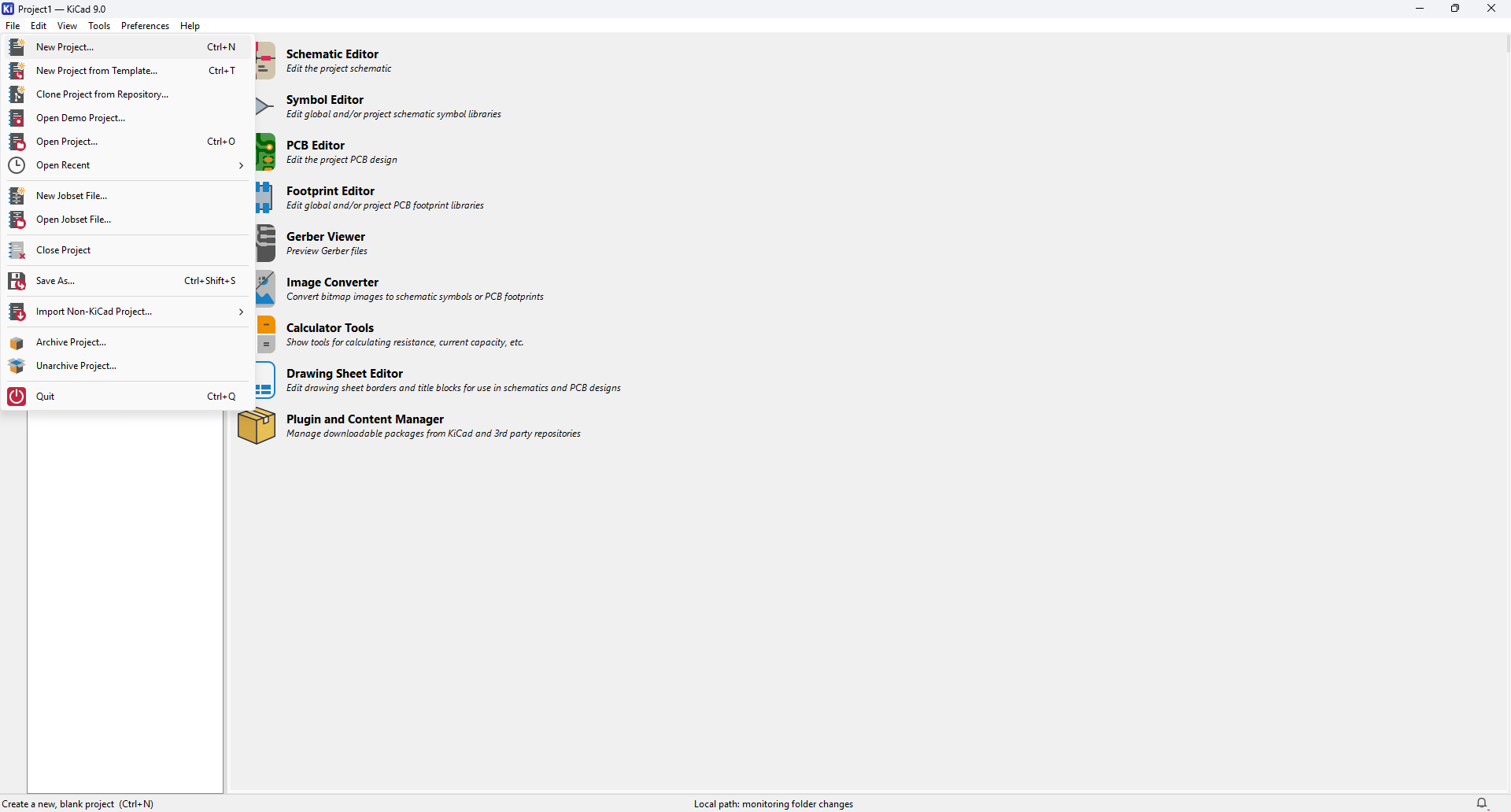
KI CAD
Ki Cad is a free software suite for electronic design automation (EDA). It facilitates the design and simulation of electronic hardware for PCB manufacturing. It features an integrated environment for schematic capture, PCB layout, manufacturing file viewing, ngspice-provided SPICE simulation, and engineering calculation. Tools exist within the package to create bill of materials, artwork, Gerber files, and 3D models of the PCB and its components.
Link : KiCad EDA - Schematic Capture & PCB Design Software
At the beginning of the class, we received basic training in KiCad, where we were introduced to the essential tools and workflow for designing electronic circuits. The session covered how to create and manage schematics, add components from the library, and import custom footprints and symbols that may not be available by default. We also learned how to properly organize and connect components in the schematic to form a complete circuit. In addition, some commonly used shortcuts and navigation tips were explained to help speed up the design process.
Apart from the training, I also explored and learned some additional techniques on my own—for example, how to import schematics from EasyEDA into KiCad. This process and the steps involved have been documented below.
Installation of KiCad and set up
- Fist step is to download KI cad from the official website from the provided link download the latest version . Download Link : https://www.kicad.org/download/
- Then next step is to install the software go to you downloads folder and open the downloaded exe file to initiate installation.
- Then open KiCad then from the top left corner go to files and new project then give a name and navigate to the location where you want to save the five a save it there
- Now open the file
- There will be two types of file on the right window Kicad_pcb and Kicad_sch
- Here the Kicad_pcb file have the design of the PCB and Kicad_sch contains the circuits for the design
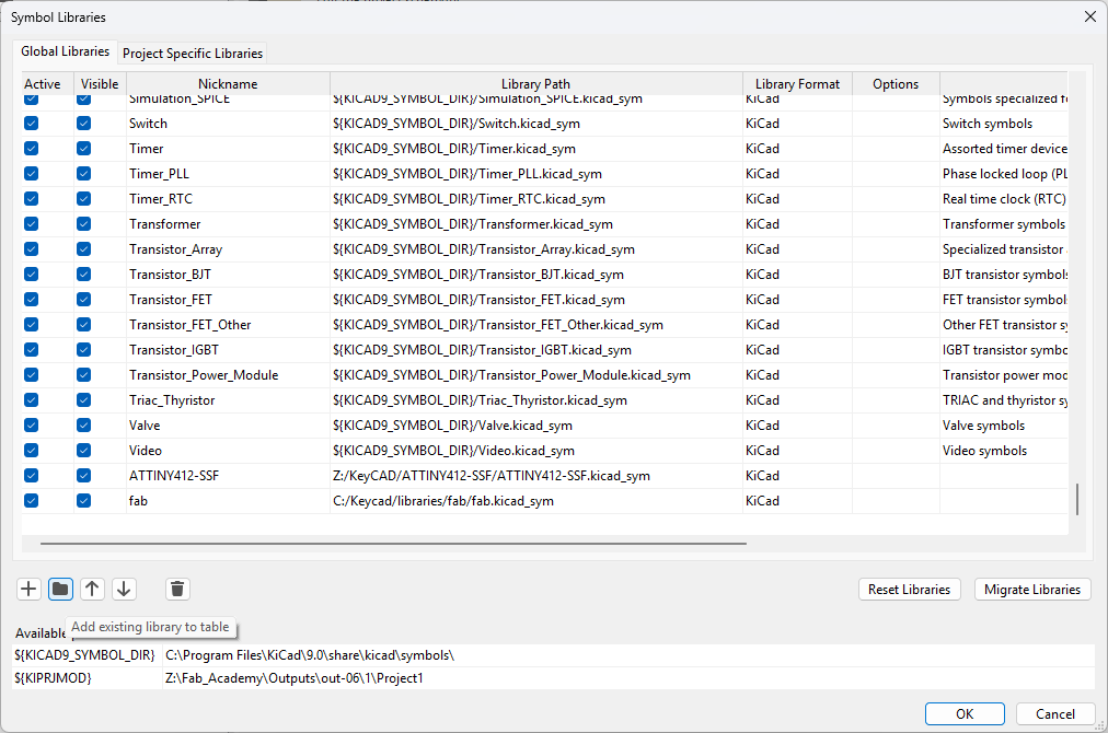
- As the next step we have to import some libraries of components made for fab academy these contains most of the components in our inventory.This was done so that all the foot prints, an schematics of the components can be added. If ther are missing download them from any website and add them to the library.
- For this clone the repo from the link provided in the link to your drive where you have installed KiCad and make a File KiCad >> Libraries and clone the repo inside this file. Link : pub / libraries / electronics / KiCad · GitLab
- Copy the SSH Key and clone the repository using git bash.
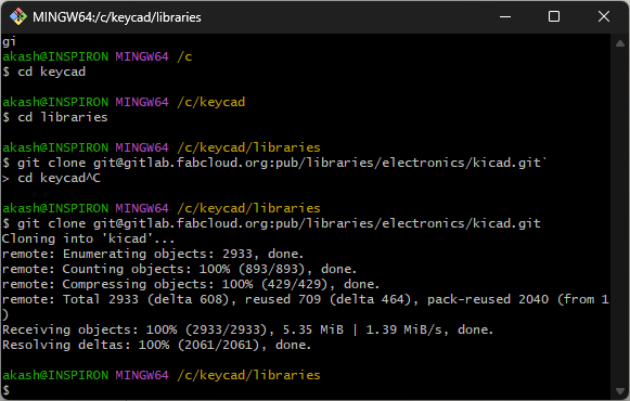
I had accidentally accidentally named the main file as key cad because of the the name in the cdm will be different.
Then from the top section in preferences in preferences
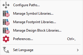
First to add symbol libraries click on the and click on the file button from the window that appears and go the file location where we cloned the repo and then select the kicad_sym file and press ok.
For the next step from preference select the footprint library follow the same step but in the last step select the file and and move on.
- Then the next step will be to select the micro controller and go through the data sheet for this trial project I am using an ATtiny412 Data sheet Link : ATtiny212 / ATtiny412 Complete
- And then in the schematic editing workspace import the components and make the basic circuit.
Schematic Editor shortcuts
- A → Add a component
- M → Move a component
- R → Rotate a component
- Y → Mirror a component
- E → Edit properties
- C → Copy a component
- Delete → Remove component
- W → Start a wire
- G → Drag a component while keeping wires connected
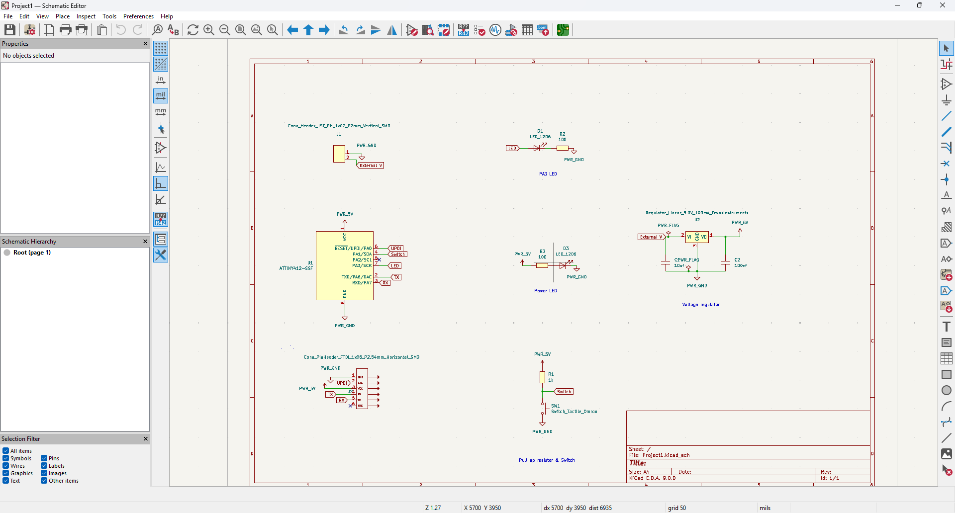
Schematic Interface
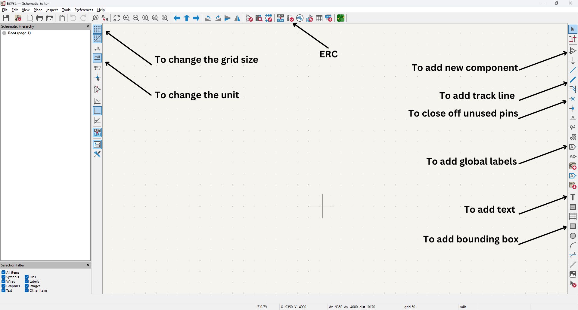
This is the basic interface of the schematic editor the tools in the right tool bar are used to make the circuit and the tools in the left tool bar are used to control the interface.the right tool bar contains tools to add new elements to the circuit, tool to draw track , tool to close of an unused pin etc, the image above can be used for getting a basic idea about the tools and the interface.
PCB Editor
- A → Add a component
- M → Move a component
- R → Rotate a component
- Y → Mirror a component
- E → Edit properties
- C → Copy a component
- Delete → Remove component
- W → Start a wire
- G → Drag a component while keeping wires connected
- D → Drag a track
- X → Route a new track
- B → Refill zones
- V → Change via size
- Ctrl + Shift + V → Paste special
- / (Forward Slash) → Switch between layers
- Shift + Space → Change track width
- Delete → Remove track or component
PCB Editor Interface
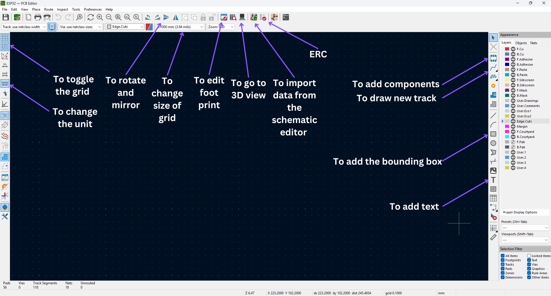
This is the basic interface of the PCB editor here on the right tool bar we have tools to add new elements to the circuit, tool to draw track , tool to add bunting box, tool to add text etc.From the top tool section we have tools to change the orientation of the components, tools to change the size of the grid, tools to edit the footprint of the components, tools to see the 3D view of the components,tools to import the schematic editor, ERC etc. In the 3D view port we can see the 3D model of the circuit.
Steps of making a circuit
1. Open KiCad and Create a New Project
- Go to File > New Project, give it a name (e.g.,
MyBoard), and choose a location. - Click Create to generate the project files.
2. Open the Schematic Editor
- In the Project Manager, click on "Schematic Editor" to open a blank canvas where you'll build your circuit.
3. Add Components to the Schematic
- Press A or click the "Place Symbol" button from the right toolbar.
- Search for a component (like
ATtiny3216,R,C,LED,Connector, etc.) and click OK to place it. - Click again in the schematic area to drop the component.
- Repeat this for all the components you need.
4. Connect Components Using Wires
- Press W or click the "Place Wire" tool.
- Click on a pin of one component, drag the wire to the pin of another component, and click to finish.
- Continue until all relevant pins are connected.
- Press Esc to exit wire mode.
5. Add Power and Ground Symbols
- Press A again, and search for
GND,VCC,+5V, or other power symbols. - Place them near your circuit and wire them to power pins.
6. Label Nets (Optional but Recommended)
- Press L to place a net label.
- Name important signal wires (e.g.,
SCL,SDA,RESET) for clarity and easier routing later.
7. Annotate the Schematic
- Go to Tools > Annotate Schematic to assign part numbers like
R1,C2,U1, etc. - Click Annotate, then Close.
8. Assign Footprints to Components
- Go to Tools > Assign Footprints.
- This opens a table to link each schematic symbol to a physical footprint (e.g.,
Resistor_SMD:R_0805). - Assign correct footprints manually or automatically.
- Click Apply, then OK.
9. Run Electrical Rules Check (ERC)
- Click Inspect > Electrical Rules Checker.
- Click Run and review any errors or warnings.
- Resolve issues like unconnected pins or missing power inputs.
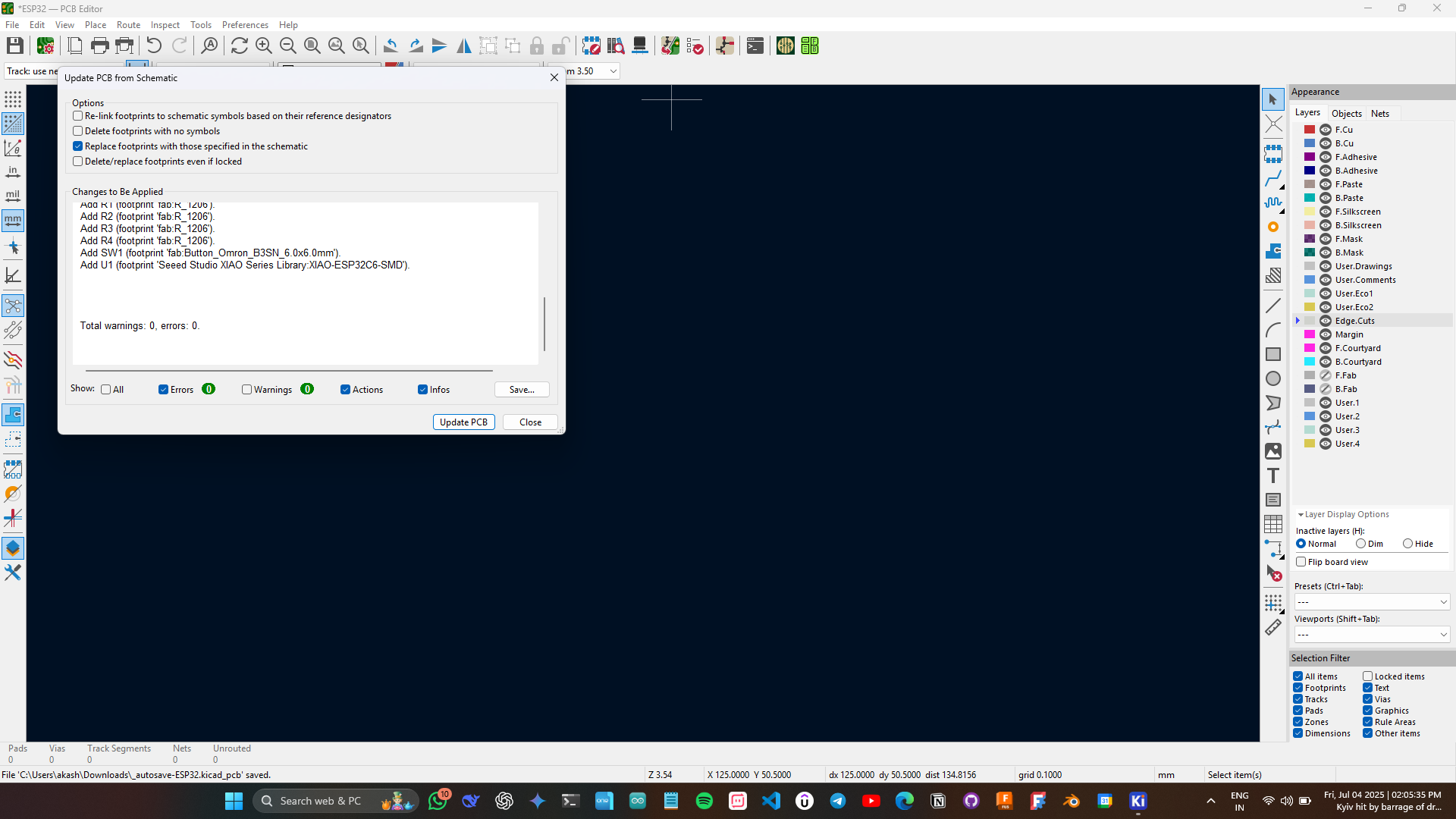
10. Update PCB with Schematic
- Click "Update PCB with changes from schematic" in the top toolbar.
- This creates a netlist and transfers all component footprints and connections to the PCB layout.
KiCad: Ground, Power Flags, and Labeling
1. Ground and Power Symbols
- Power Symbols (like
+5V,VCC) represent voltage sources. - Ground Symbol (GND) represents the 0V reference in your circuit.
- These are global nets — no need to wire everywhere.
2. Power Flags
- Used to tell KiCad that a power net is actually powered.
- Prevents ERC errors like "No power source on net".
- Place
PWR_FLAGon power and ground nets.
3. Net Labeling
- Labels connect wires without drawing long lines.
- Press L and type a name (e.g.,
SDA,TX). - All wires with the same label are automatically connected.
- Use labels for clarity and cleaner schematics.
KiCad PCB Editor Guide
1. Arrange Components
- After importing the schematic, open the PCB Editor.
- Drag and drop components onto the board area.
- Use M to move and R to rotate parts.
- Keep related components close for clean routing.
2. Define Board Outline (Edge Cuts)
- Select the Edge.Cuts layer.
- Use the “Add Graphic Line” tool to draw the outline.
- Ensure the shape is closed — rectangle or custom shape.
- This defines the physical size of your PCB.
3. Route the Traces
- Press X to start routing traces.
- Click from one pad to another to create copper connections.
- Use 45° angles instead of sharp 90° turns.
- Use vias (V) to change PCB layers.
- Top layer is usually red; bottom is blue.
4. Finalize and Check
- Run the Design Rule Check (DRC) to find errors.
- Add copper fills (e.g., ground planes) with the "Add Filled Zones" tool.
Designing My First Schematic and PCB in KiCad
To begin designing my circuit, I opened KiCad and created a new project. The first step was to open the schematic editor and add the essential components. I started by placing a microcontroller (ATtiny3216), which would serve as the heart of my circuit.
After that, I added supporting components like a capacitor, resistor, and LED. To add components, I used the "Place Symbol" tool and searched for each part in the library. If any symbol or footprint was missing, I used the symbol library editor to import or create it manually.
I then used the "Wire" tool to connect the components. To make the schematic easier to read, I also added labels for each net. For example, I labeled the power and ground lines as VCC and GND to avoid cluttering the schematic with too many wires.
Schematic View
Below is an image showing the initial schematic layout after connecting the microcontroller and other components:
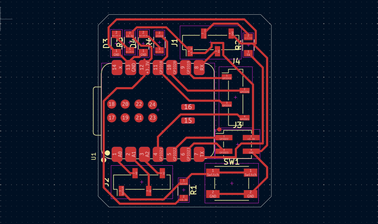
Converting Schematic to PCB Layout
After completing the schematic, I clicked on the “Update PCB from Schematic” button (symbol: a schematic with an arrow). This transferred all the components into the PCB editor. Initially, the components are placed randomly on the canvas.
I then arranged the components manually to match my desired board shape. I tried to keep related components close to minimize trace length. After positioning the parts, I used the “Route Tracks” tool to draw the copper connections between the pins. I also defined the board outline using the “Edge.Cuts” layer to create a custom board shape.
Final PCB Layout
Here is the final routed PCB layout after placing and connecting all components:
Created using Chatgpt
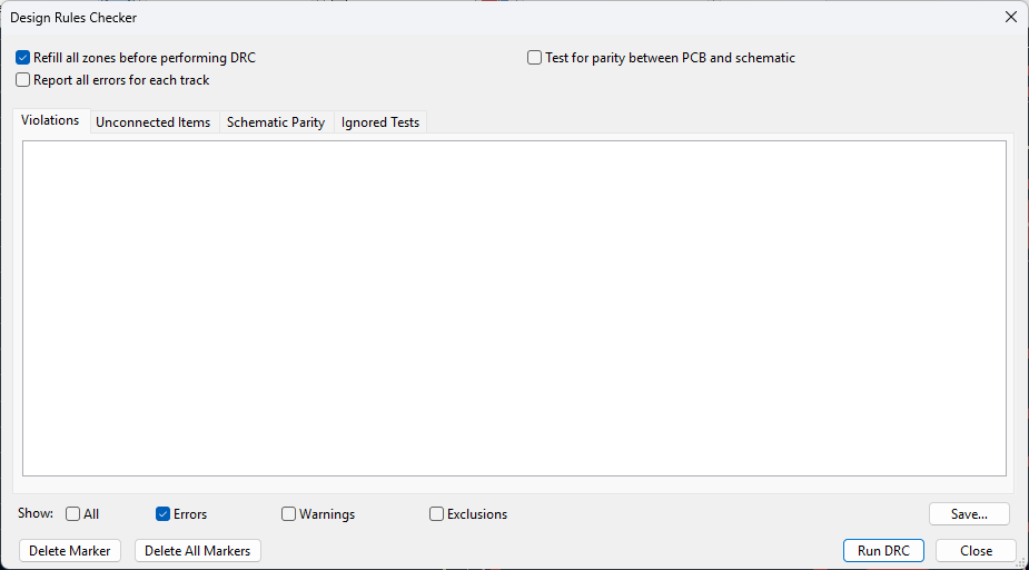
Electrical Rules Check (ERC)
In KiCad, the Electrical Rules Check (ERC) is a tool used to verify the schematic for electrical design errors. It helps detect issues such as unconnected pins, short circuits, power conflicts, and input/output mismatches. It also identifies multiple power sources on the same net and checks that output pins are not directly connected to each other.Open the Electrical Rules Check dialog from the top tools menu.then run the ERC which will show the errors. Also make sure to add flags to ground and power or else this may cause an error.
- For learning about interface of Kicad and to learn watch the video tagged below. Link : https://www.bing.com/videos/riverview/relatedvideo?q=Kicad+using+documentation&mid=699C25CE8AA6202B7AF7699C25CE8AA6202B7AF7&FORM=VIRE
- After this make the circuit need in the schematic editor work space.
while designing makes sure that all the components that we are using for the design is available in the inventory. For this our amazing team of developers in super fab lab kochi have created a an amazing website for tracking the inventory of fab lab kochi.
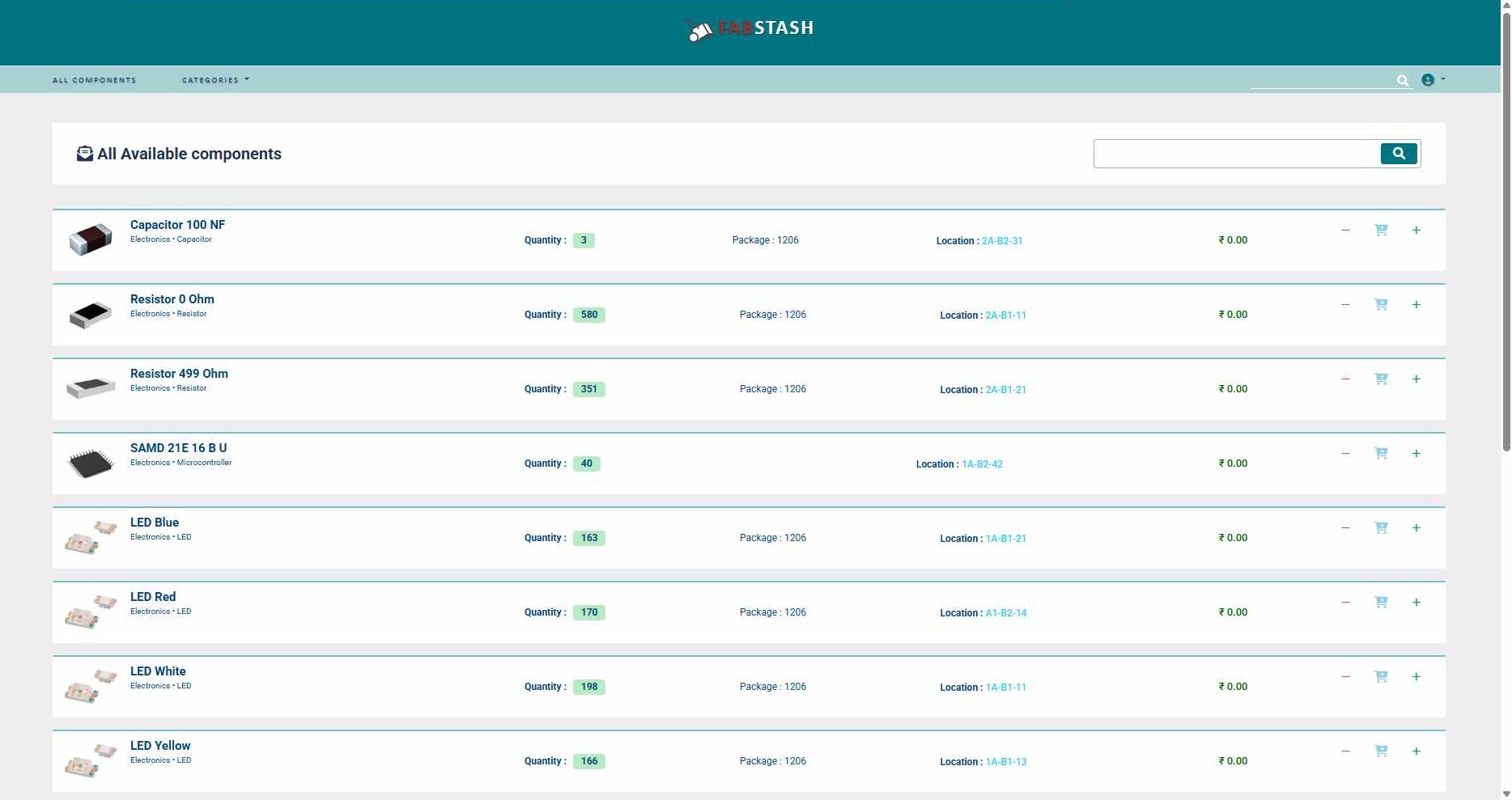
Link : Fab Lab Kochi Inventory
- For finding the resistor needed for the LED I calculated the value of resistance using the ohms law.
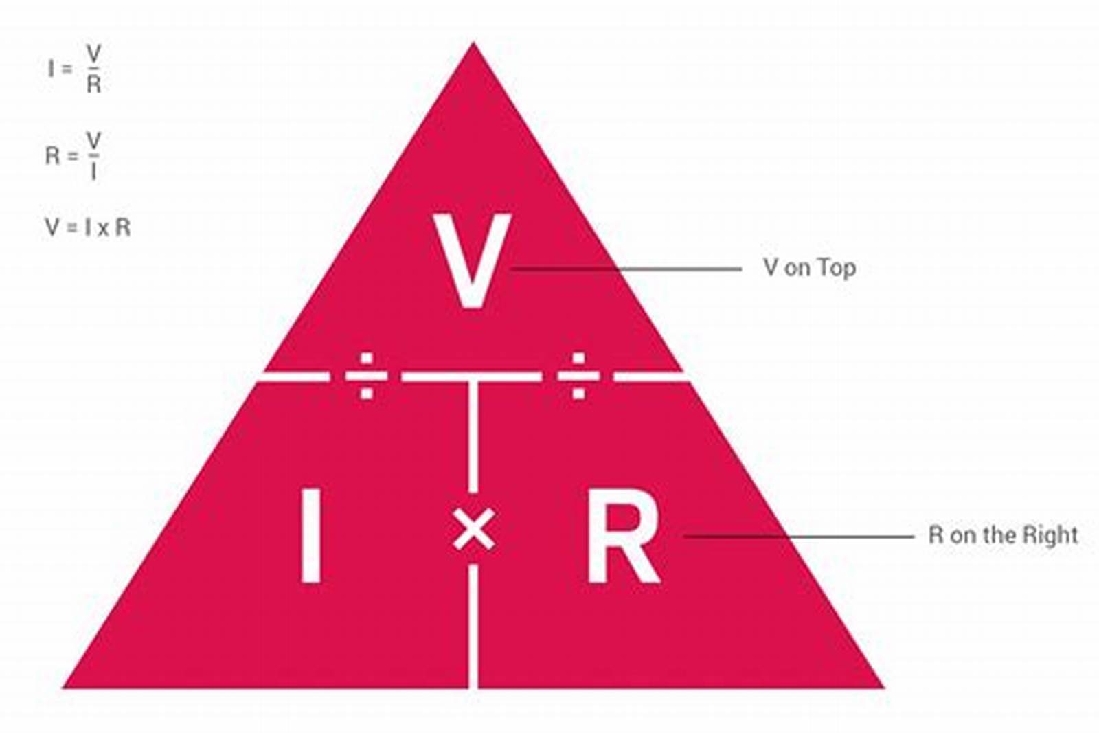
Image Source:https://solderingmind.com
- Ten from the top tool bar click on the Electrical rules checker to check if every connection hade been made if if shows any errors check through it make the necessary corrections.
- when there are no errors go into the PCB Editor workspace.
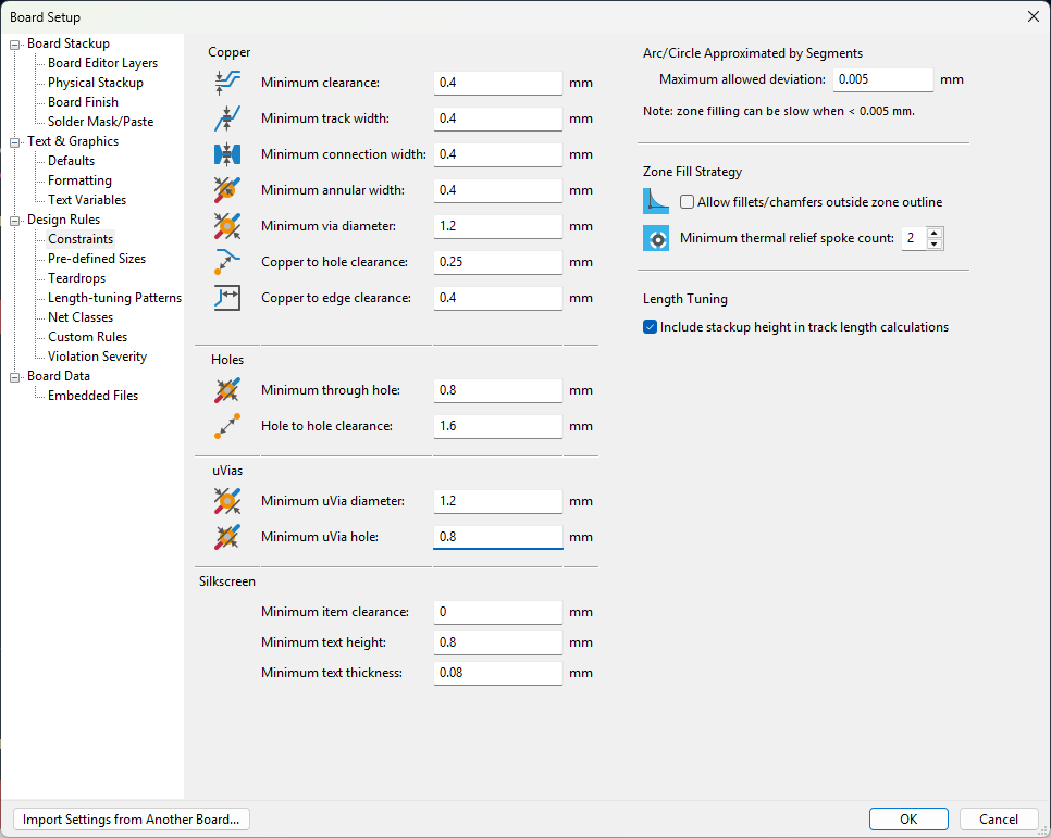
- In the PCB workspace first go the Bard setup from the top tool bar and add the parameters depending on the capability of the machine available.
- I changed the parameters so that it matches the capability of the machine available in our lab.
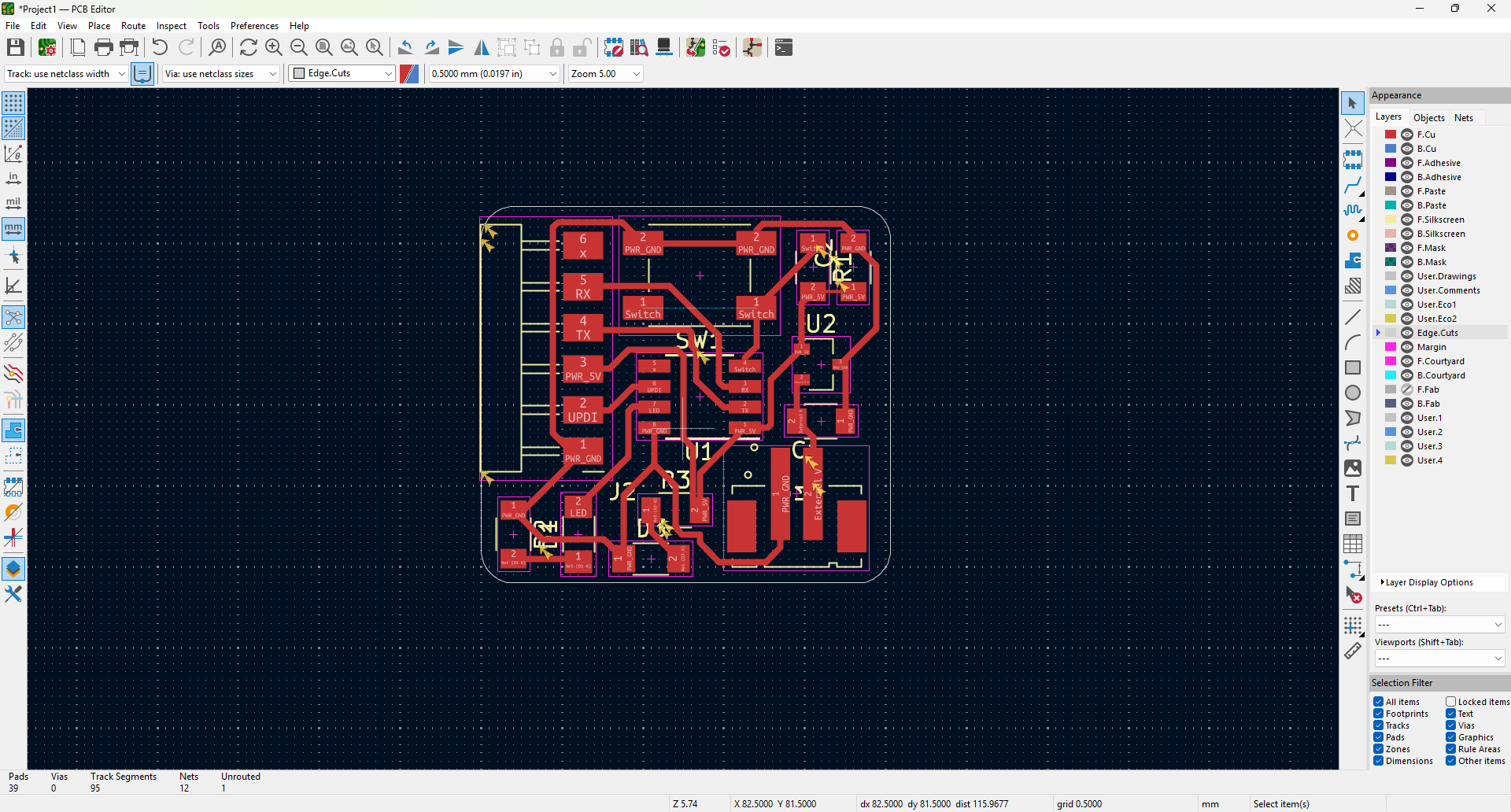
- Then arrange the components in a way that the number connection's overlap is less
- Then using the tools make the necessary connections then from the top tool bar use the design checker tool and make the corrections and confirm the design.
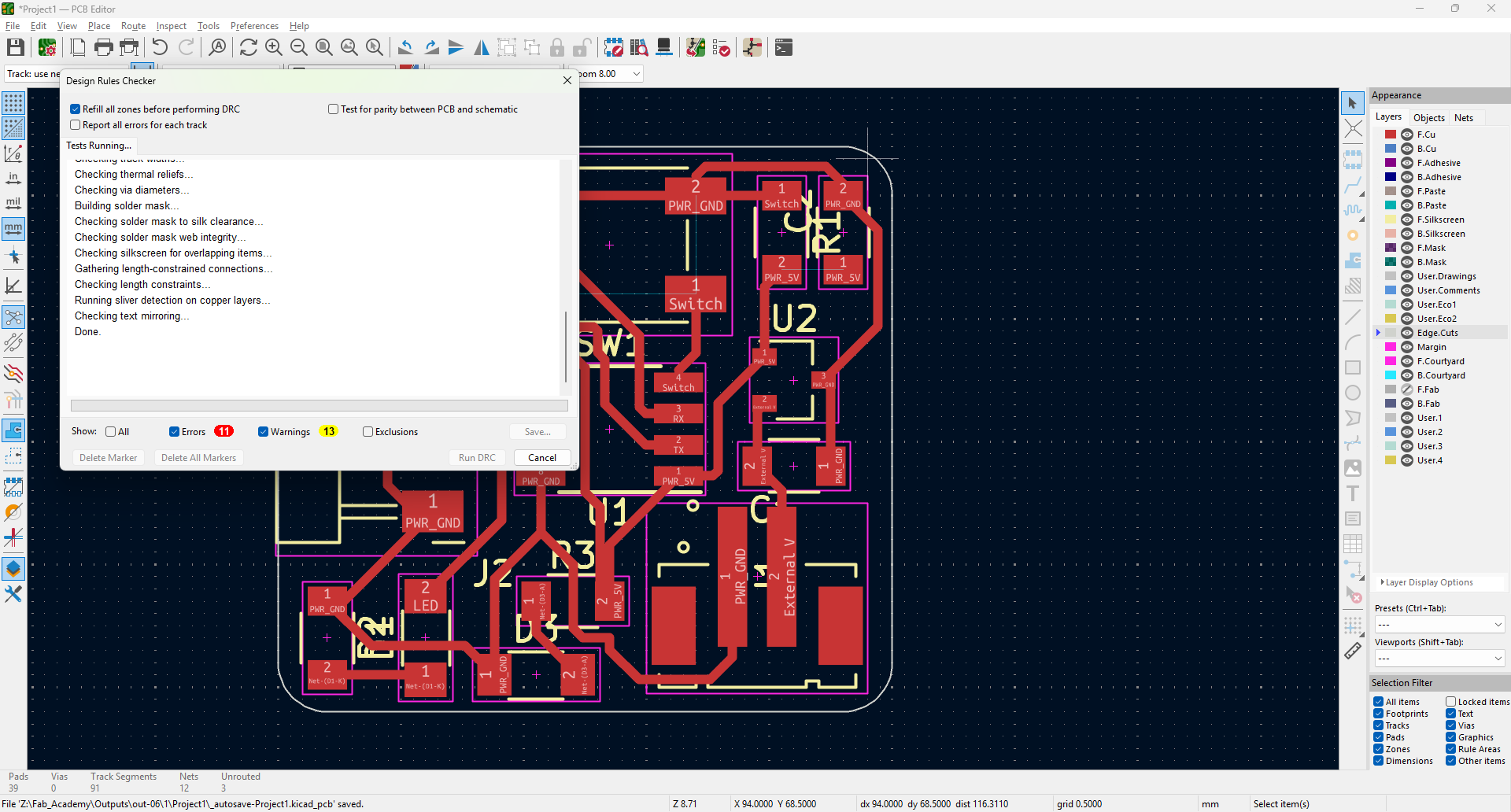
Then when there were some errors the red errors are more important so those were errors like the traces are to close to the ede or if some components are missing in the design or sime lines are not connected etc so i had to make the necessary corrections and confirmed the design
- Then finalized the design when there are no errors in the design.
- Then to add 3D design components select he component in the components in the PCB editing section then right click and in the 3D model section hover over the file path and select the location of the file ie, inside the library section go into the file which contain the step file and then select the component's step file.
- If the model is not properly arranged use the tools available on the side bar in this window to adjust the scale or Rotation or the Offset.
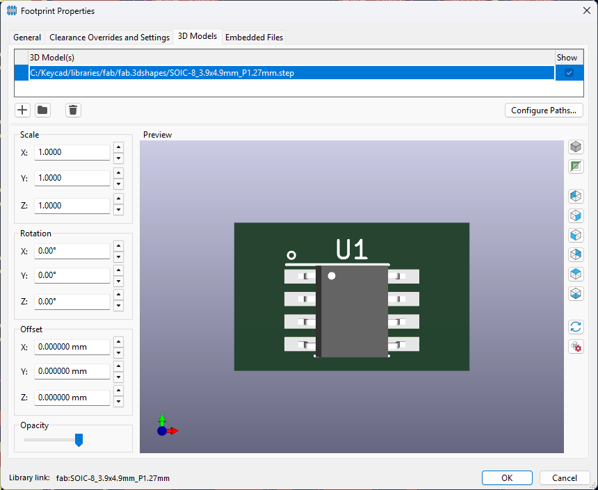
- Then import all the 3d files and assign it.
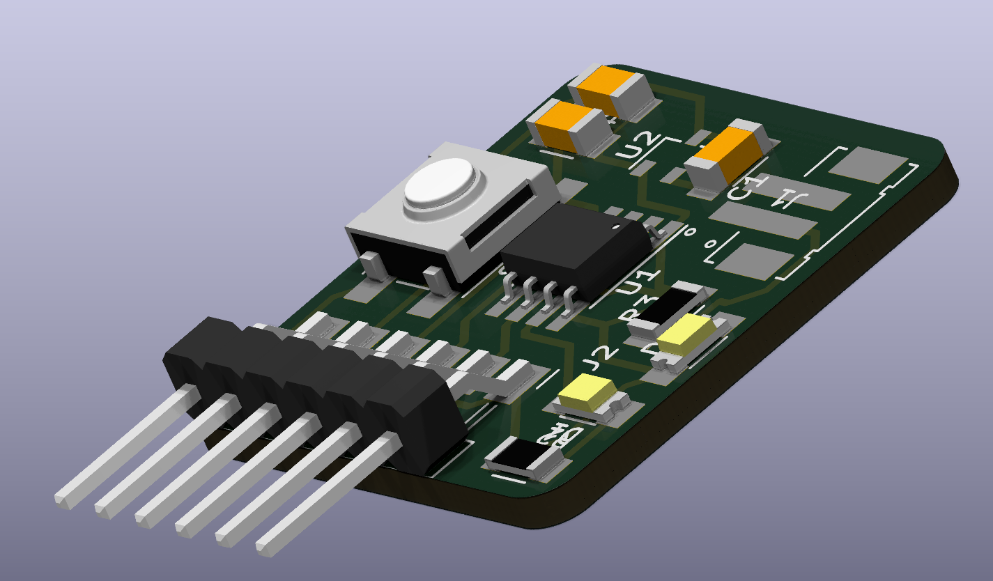
- This is the final out put. 3d design for some components were not available in the library if needed the file should be downloaded from other websites.
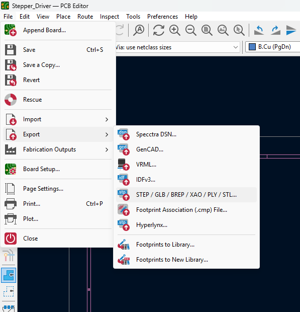
Exporting the PCB design
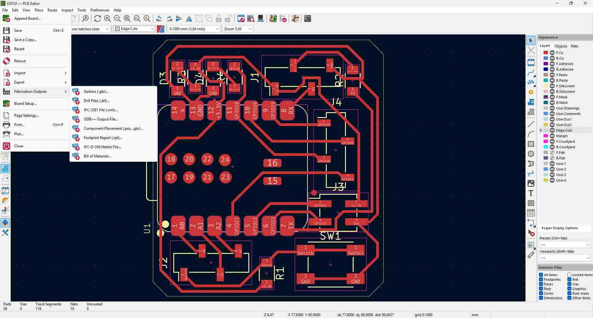
For exporting a pcb design From files go to fabrication Output and export as gerbers.
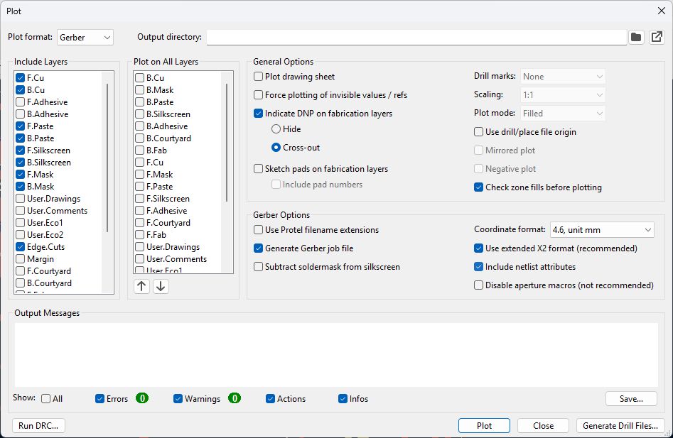
And from the window that appears click plot and all the files will be saved to the file if you give a output directory name the file wll be saved as a single folder with the name you entered, if you are making a multilayer pcb with holes press the generate drill files switch to generate the file for making the holes.These files that we received can be shared for PCB manufacturing.
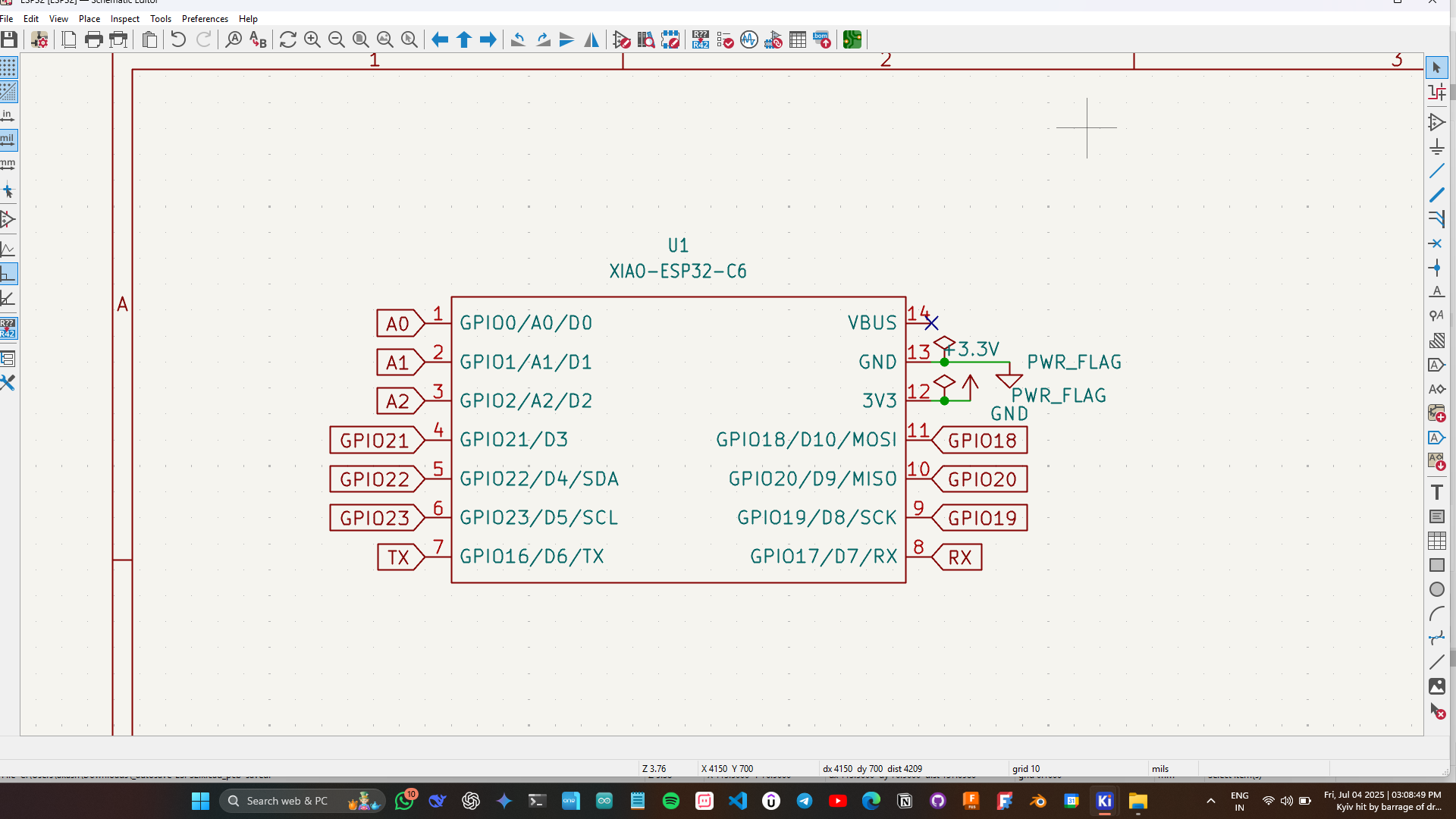
Custom board With XAIO
Here my plan was to make a custom board with an XAIO ESP-32 C6 mounted on it with all the GPIO Pins, TX & RX Pins,I2C and Analog pins taken outside with pin slots . For this I started by referring the data sheet of the micro controller to learn about the micro controller and its outputs
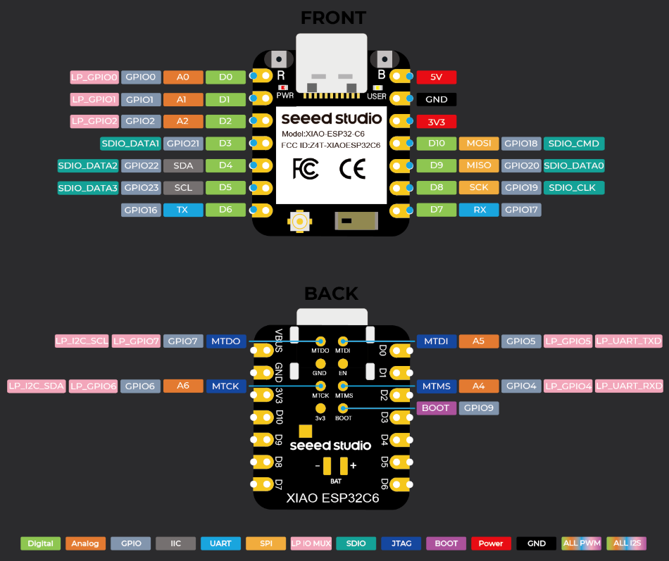
Link : Getting Started with Seeed Studio XIAO ESP32C6 | Seeed Studio Wiki
Schematic Design
First i started by making the schematic of the board using the KiCad.
I started by opening the schematic editor and then using "A" shortcut to add componets into the schematic
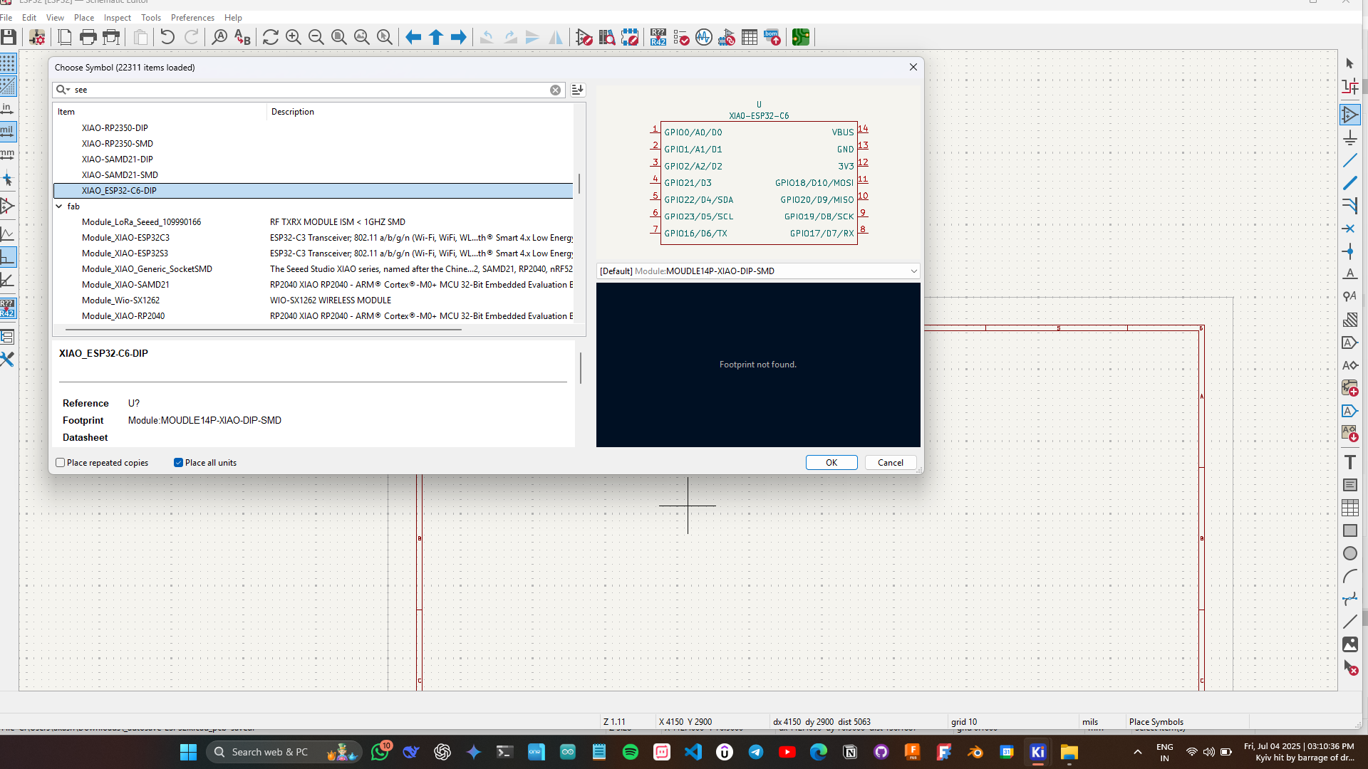
Then i added the microcontroller XAIO ESP-32 C6 in to the schematic.
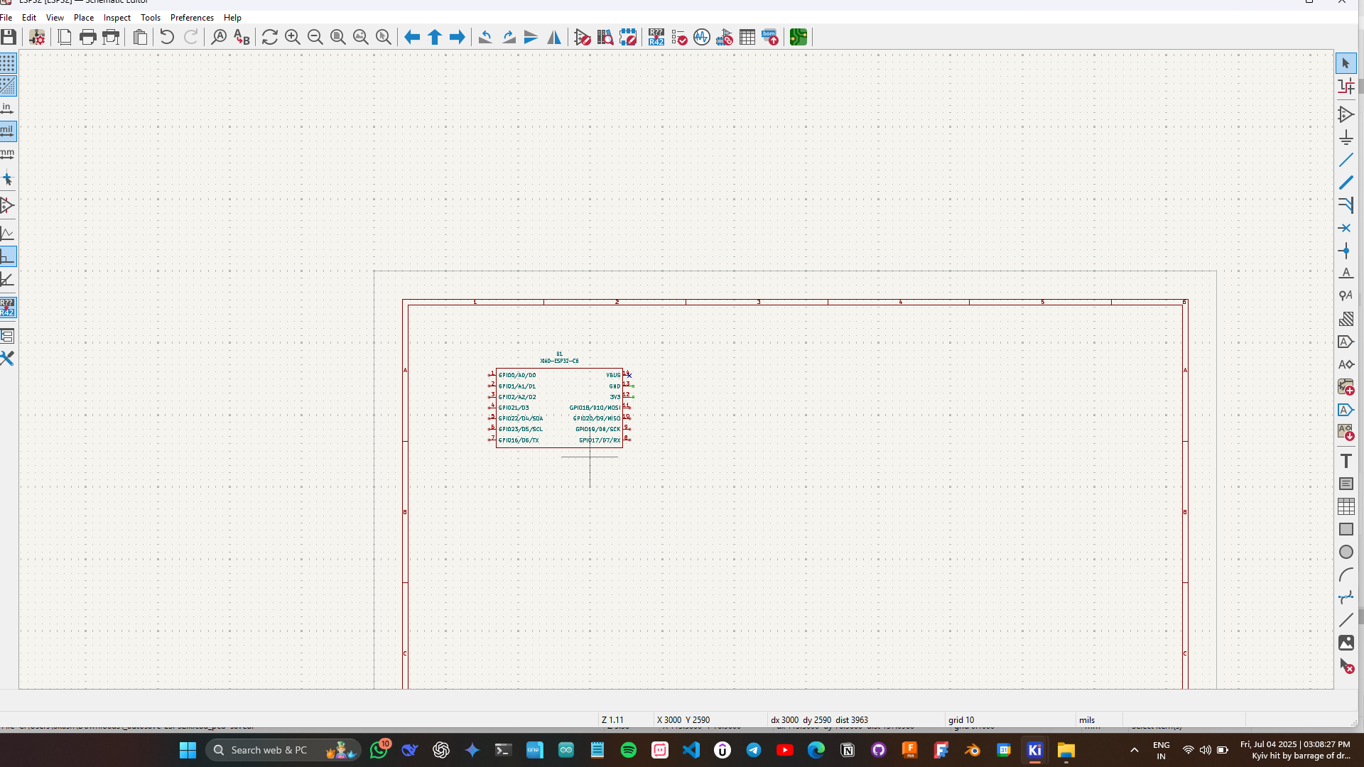
Then as the next step added all the pins including the programmer pins and all other output & Input pins.
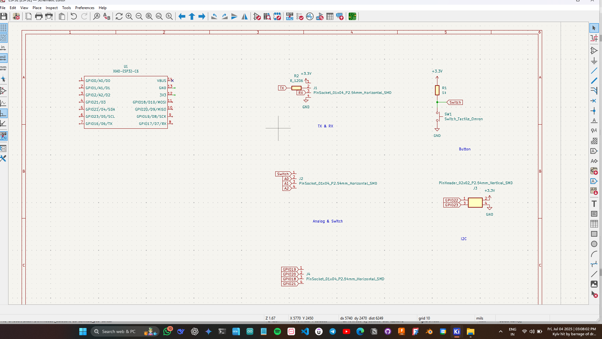
Then as the next step i added all the LEDs for Power indication and one LED for programming.
Then as the next step i added all the labels for all the pins as needed also confirmed it with the data sheet. also added the power flag ,power and ground lines.
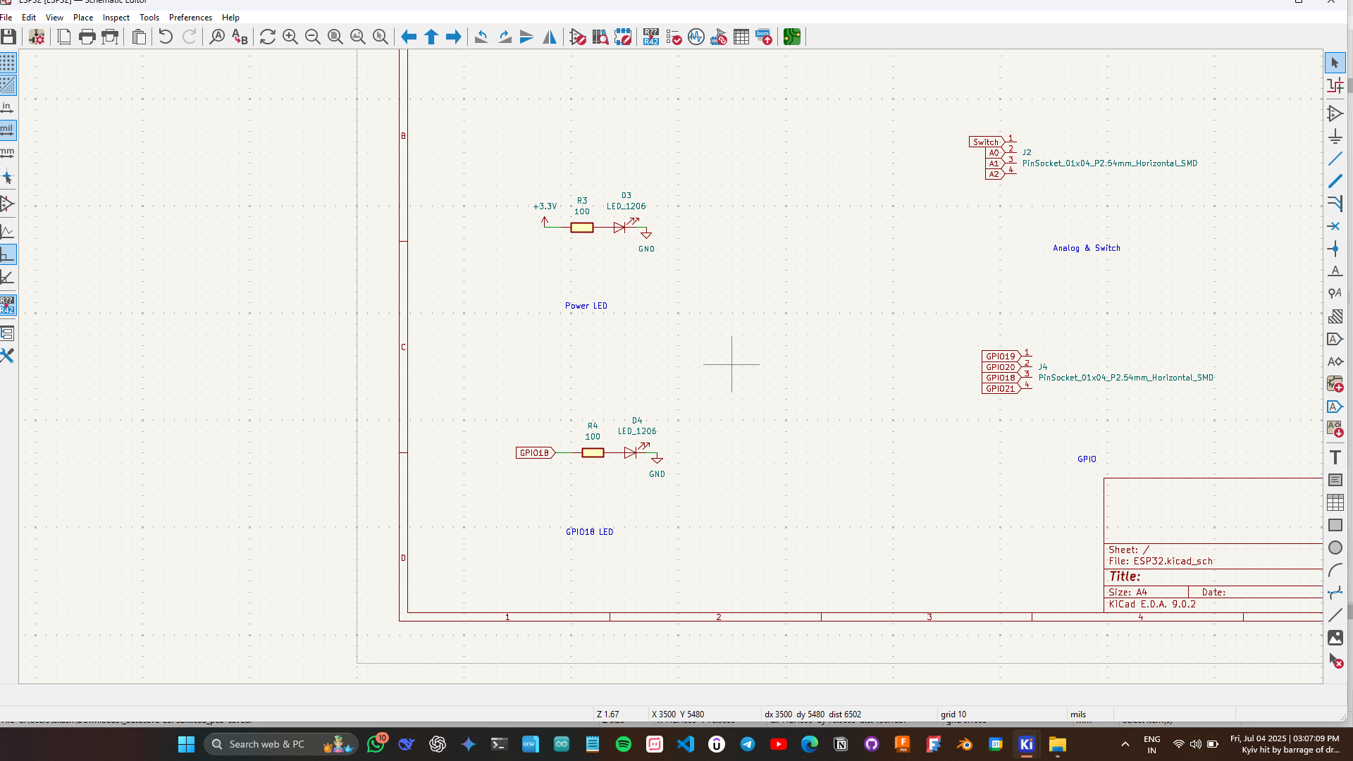
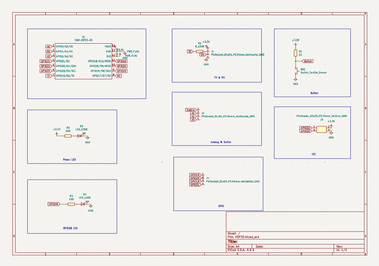
Then i made the schematic of the organized with boxes separating the components. and this is the final schematic.
PCB Design
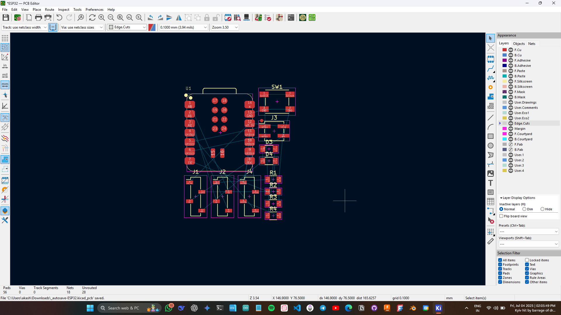
Then from the top tool bar i went into the PCB editor window i pressed the import all components from the schematic into the PCB editor work space.
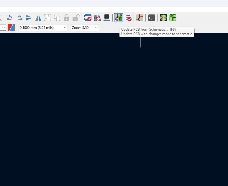
Then press the "Update PCB " button to import all the components from the schematic into the PCB editor.
This is the initial PCB layout after importing all the components from the schematic.
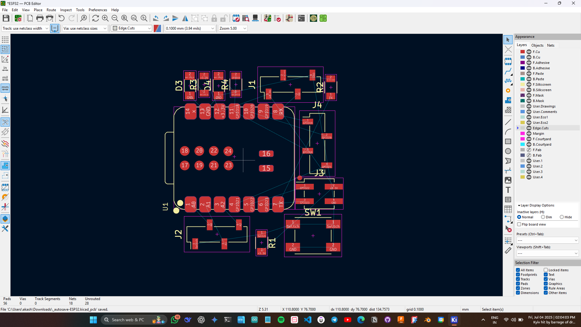
Then i arranged the components in a way that the connections are less and the components are arranged in a way that it is easy to connect them.
Then i started connecting the components using the "Route Tracks" tool in the right tool bar.
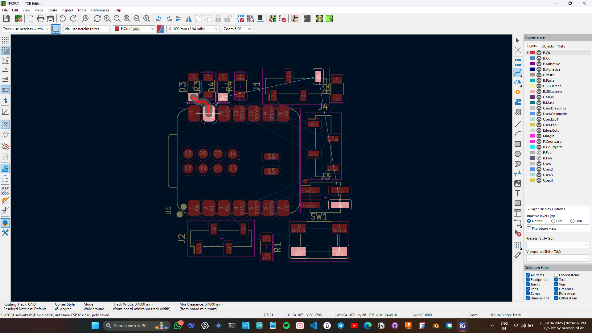
Just for the fun part i made sure note to use vias or bridging resistors to connect the components.
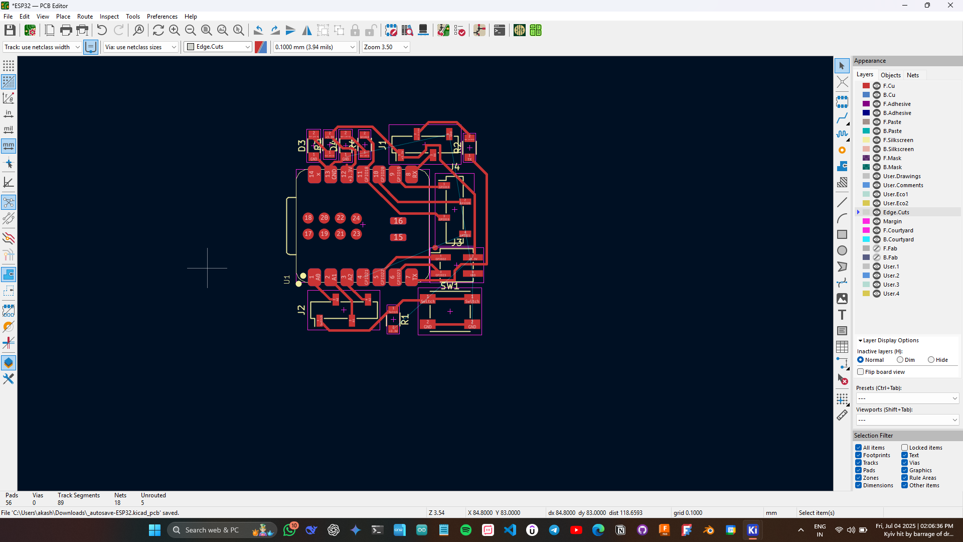
And this is the final pc design for the board
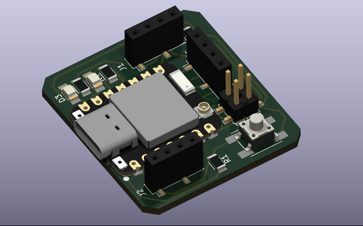
Then I went into 3D View and rendered it to get the final result since the 3D file the micro controller was not with the file I downloaded from the Seed studio, I downloaded the file from and external website
Link : Seeed Studio XIAO ESP32C6 | 3D CAD Model Library | GrabCAD
And this is the final output
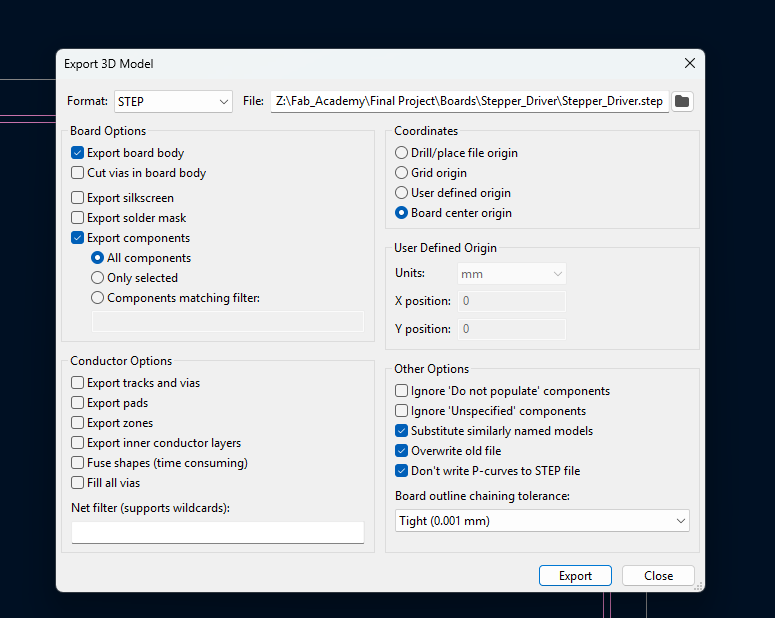
From the top left corner in the file section goto export and select step.
Then select select the needed .
Then in fusion from the left tool bar click the upload button
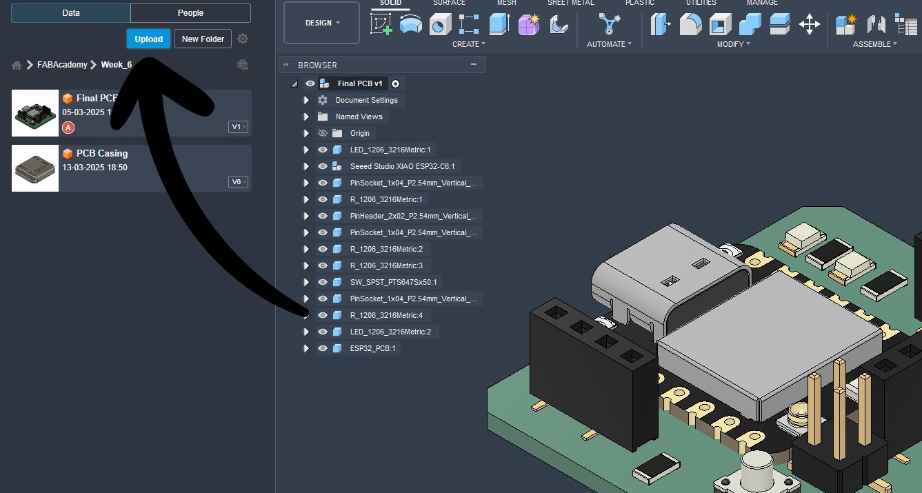
Then from the window that appears select the files that you want to upload and then the file will be uploaded and it will appear in the left section and can be edited or imported to another design.
Then I imported this this into the file and designed a simple PCB Enclosure and also added holes for LED's and slots fo the pins and the USB Port.
Conclusion
This week's assignment focuses on both practical observation and design. As a group, we will use the test equipment in our lab to observe the operation of a micro controller circuit board, gaining hands-on experience with real-time analysis. Individually, we will utilize an EDA tool to design a development board that incorporates components from the inventory, enabling interaction and communication with an embedded micro controller. For those aiming for extra credit, an additional challenge is to design a protective case around the development board, integrating functionality with aesthetics.