Assignment 9: Input Devices
Group Assignment
Probe an input device's analog levels and digital signals.Individual Assignment
Measure something: add a sensor to a microcontroller board that you have designed and read it.
Schematic and Components
Overview
This is the final schematic of my custom ESP32-C3-based interface board, designed in KiCad. The board uses the Seeed Studio XIAO ESP32-C3 microcontroller and provides connection headers for an external SG90 servo motor and a limit switch. It also includes an onboard status LED and proper power routing. All external components connect via SMD 0.1” tin-plated pin headers, keeping the board modular.
Final Schematic
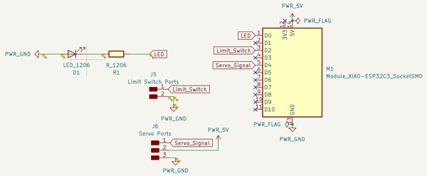
Components Used on the Board
| Component | Designator | Description |
|---|---|---|
| ESP32-C3 Module | M1 | Seeed Studio XIAO ESP32-C3, Socket SMD mount |
| SMD LED (1206) | D1 | Onboard status/debug LED |
| Resistor (1000Ω, 1206) | R1 | Current-limiting resistor for LED |
| 2-pin SMD header | J5 | Connector for external limit switch |
| 3-pin SMD header | J6 | Connector for external servo motor |
Connector Mapping
J5 – Limit Switch Port
- Pin 1 →
Limit_Switch(GPIO2) - Pin 2 →
PWR_GND
J6 – Servo Port
- Pin 1 →
Servo_Signal(GPIO3) - Pin 2 →
PWR_5V - Pin 3 →
PWR_GND
Power Flags
I added PWR_FLAG symbols in KiCad to explicitly declare the 5V and
GND nets as valid power sources. Without these flags, the Electrical Rules Check (ERC)
would throw errors, assuming these power nets are floating. This ensures ERC validation passes.
“X” Symbols on Unused Pins
On the ESP32-C3 symbol, unused pins are marked with an “X” symbol. This tells KiCad that these pins are intentionally not connected and suppresses ERC warnings. This is a clean and safe practice to avoid noise or confusion in the schematic.
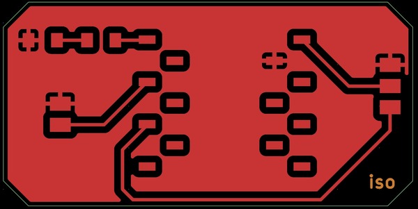
PCB Design and Layout
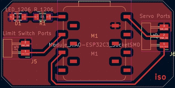
Component Placement Strategy
The placement of components was carefully considered to ensure efficient routing and usability. The Seeed Studio XIAO ESP32-C3 was placed at the center to minimize trace length. I placed the limit switch header and LED on the left side, and the servo header on the right to isolate power-heavy components from signal-sensitive ones. I also included a small silkscreen signature ("iso") on the bottom right for personalization.
Routing and Copper Zones
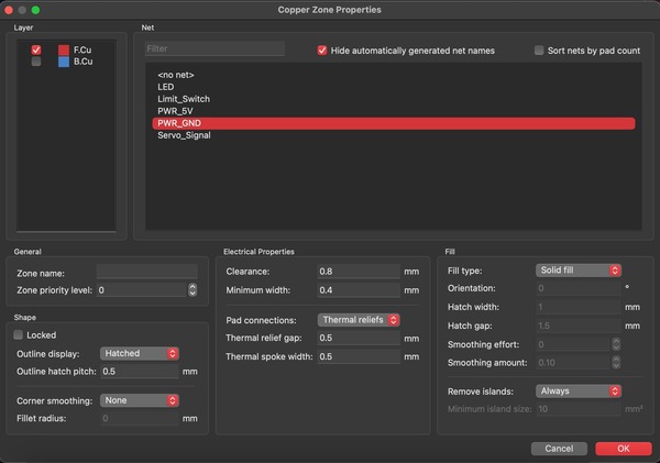
After finalizing the schematic and confirming no ERC errors, I started routing the board. Initially, I used 0.2mm wide tracks, but I later increased them to 0.4mm to improve current flow and reduce resistance. I created a ground copper zone (GND island) using the PWR_GND net to ensure better ground connectivity across the board. This zone was defined with the following electrical properties:
- Clearance: 0.8 mm
- Minimum width: 0.4 mm
- Pad connections: Thermal reliefs
- Thermal relief gap: 0.5 mm
- Thermal spoke width: 0.5 mm
- Fill type: Solid fill
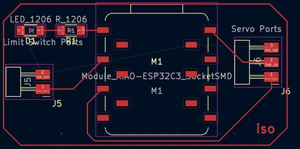
Edge Cuts and Board Outline
Initially, I drew the outline on the copper layer by mistake, which triggered a DRC error. I corrected it by redrawing the outline on the Edge.Cuts layer. This properly defines the board shape for fabrication tools.
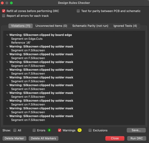
Design Rule Check (DRC)
After updating the outline and routing, I ran a DRC check. All errors were resolved, and the remaining warnings were related to the silkscreen overlapping with solder mask areas. Since I was not planning to use silkscreen printing, I ignored these warnings and proceeded.
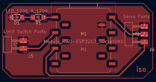
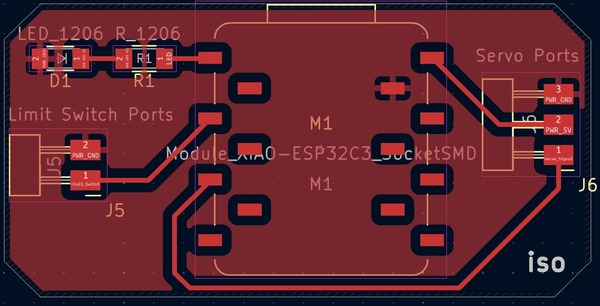
Final Board Layout
The final board layout includes proper routing, adjusted trace widths, a ground plane, and the finalized outline and labels.
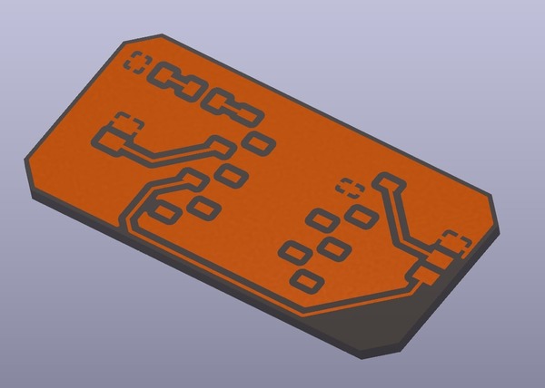
3D Rendered Model
I used KiCad’s 3D viewer to render a realistic model of my board. This helped me visually verify component placement, pad access, and routing quality.
Gerber Export and Verification
I exported the Gerber files for all relevant layers and inspected them in a Gerber viewer. Everything aligned as expected and no graphical or format errors were found.
Download Files
Download this weeks files below:
📦 Download files .) (ZIP)