KiCad Electronics Design
Assignments
Group assignment: use the test equipment in your lab to observe the operation of a microcontroller circuit board
Individual assignment:use an EDA tool to design and check a development board that uses parts from the inventory to interact and communicate with an embedded microcontroller
KiCad Installation
To install KiCad, I navigated to kicad.org and went to the Downloads section. I selected the version that matches my operating system (macOS in my case). I then ran the installer and followed the setup prompts. The process was straightforward and completed without any issues.
Introduction to the Project and Electronic Components
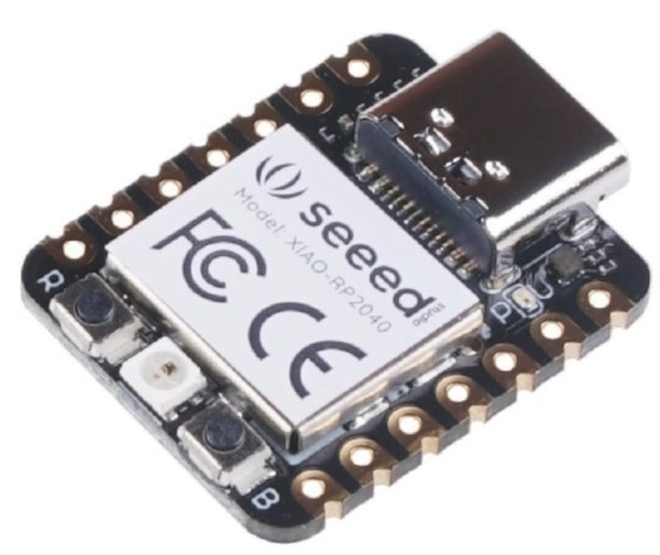
1. RP2040 Microcontroller (XIAO-RP2040)
This microcontroller is the "brain" of the circuit, running the code and controlling the connected components. It has multiple pins to interface with sensors and other devices via the I2C protocol. It is powered by both 3.3V and 5V lines, providing flexibility for a variety of components.
2. Push Button (SW1)
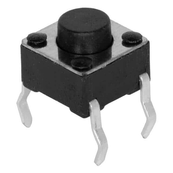
This component acts as a simple on/off switch. When pressed, it sends a signal to the microcontroller.
3. I2C Connectors (J1 and J2)
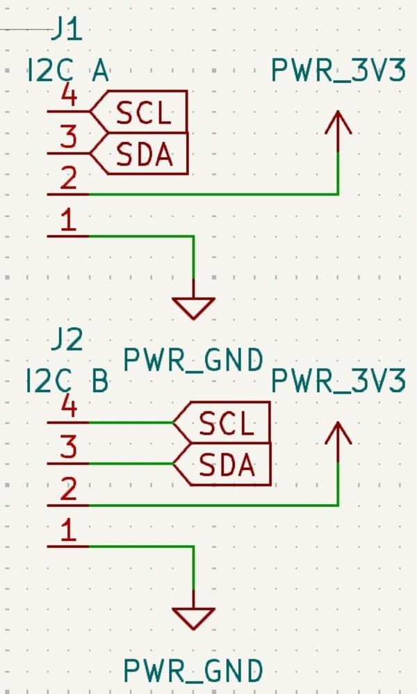
Used for module-to-module communication, the I2C connector facilitates data exchange through two lines: one for the clock (SCL) and one for data (SDA). These lines are connected to 3.3V for stable signal transmission.

4. Resistors and LEDs (R1, R2, LED1, D1)
Resistors are used to control current flow in a circuit, preventing components like LEDs or microcontrollers from being damaged by excessive current. This project is all about building identical boards that can talk to each other and work together. Each board will have the same setup, allowing for synchronized operation through I2C signals.

Schematic Design
I started by inserting the microcontroller module's footprint into the schematic:
I renamed the components to minimize space and ensure clarity:
Next, I assigned power ports to global variables:
To check for connection mistakes, I added PWR_FLAGs—KiCad's unique feature for simulating errors in connections:
I also included global labels for the microcontroller's connections:
For the ports I didn't use, I placed "no connection" flags to ensure that KiCad simulations work as intended:
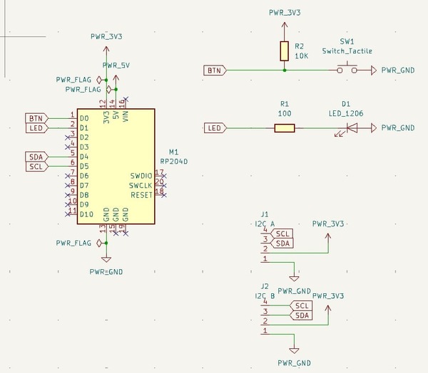
I then added two I2C connectors for communication with the other boards. I renamed them I2C A and I2C B, as shown below:

In line with KiCad conventions:
- Power input is placed at the top of the page.
- Power output is placed at the bottom.
- Signal inputs are to the left.
- Signal outputs are to the right.
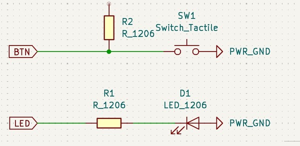
I modeled the LED and button system, assigning appropriate resistance values through the "properties" section:
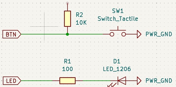
Resistor Details:
- R1: Limits current to the LED to prevent it from burning out. Its value was calculated using Ohm's Law: V = IR. With the available resistor near 75Ω, I selected 75Ω for the resistor.
- R2: Stabilizes the signal from the button. This pull-up resistor, with a typical value of 10kΩ, ensures stable circuit operation with minimal current consumption.
Final Schematic:
PCB Layout: Challenges and Workflow
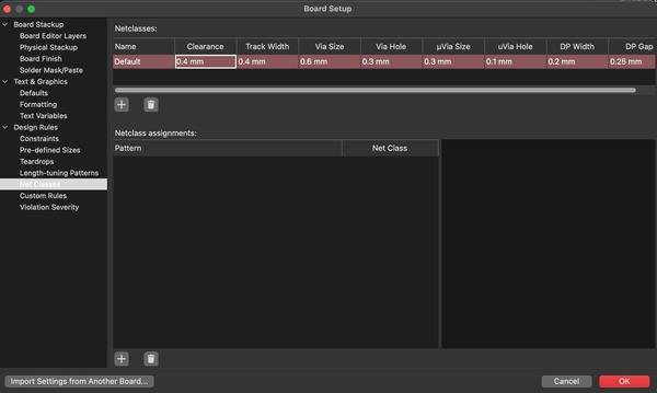
Once the schematic was ready, I transitioned to the PCB Editor. I started by adjusting clearance and track width settings based on our tool bit sizes:
I began selecting component placements and connecting the rat's nest randomly. Initially, it seemed fine, and I outlined the PCB with a rectangle using the edge cuts layer. I then added M3 bolt holes in the schematic, updated the PCB, and placed them at the corners.
After running the Electrical Rules Check (ERC), I encountered an issue with connecting the ground parts:
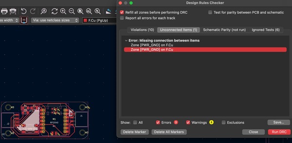
Unable to resolve the issue right away, I revisited my pre-planning and diagrammed the components, their inputs, outputs, and connections. By sticking to the revised plan, I was able to resolve the issue and complete the layout.
Final PCB Layout:
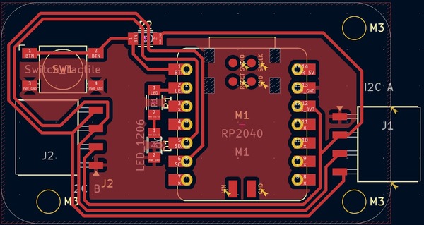
Engraved PCB:
.jpg)