Week_8 Assignments
- Group assignment:
- Individual assignment
Our group assignment was to characterize the properties of the milling PCBs "Printed Circiut Boards".
Let's just we need to design and fabricate a PCB.
Group assignment
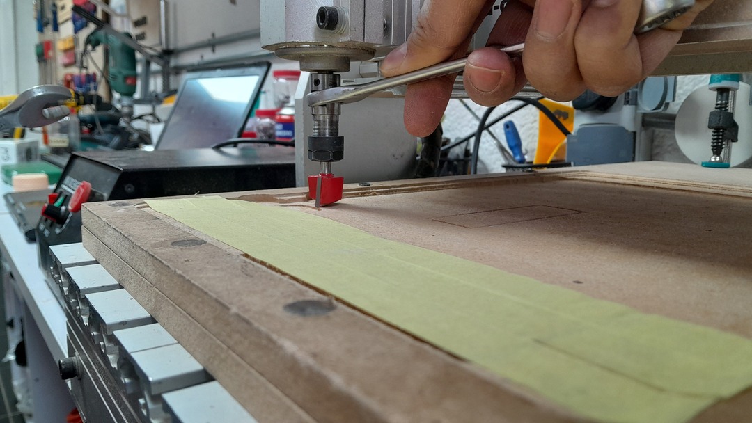
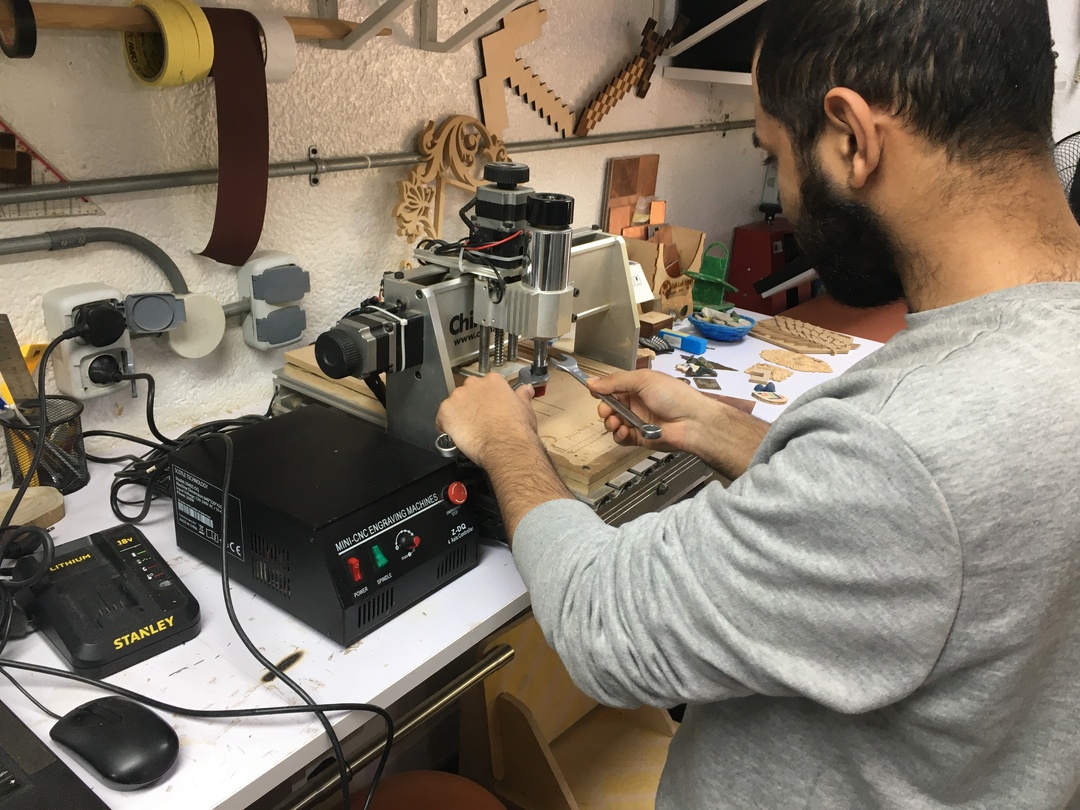
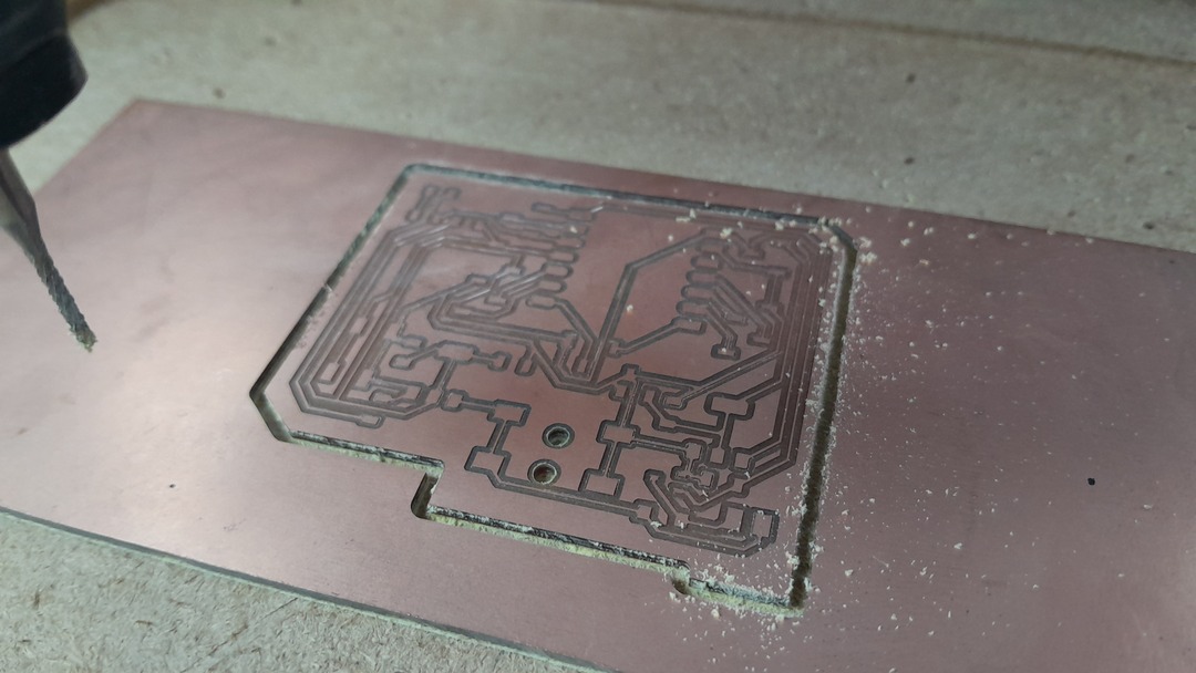
For testing our machine we started by surfacing the bed. We fixed a surfacing endlill to the machine and started surfacing.
 \
\
After surfacing is done.
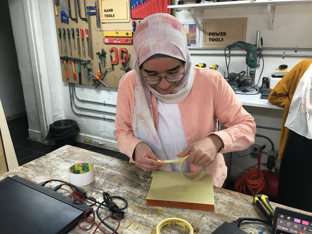
To fix the FR1 board to the sacrificial board with double face tape. But before adding the double face tape we use the yellow paint tape to make it easy for removal.
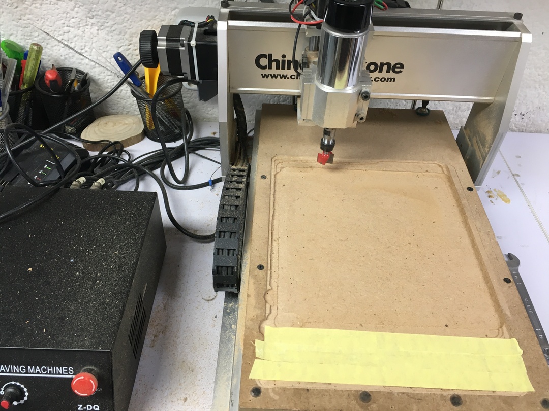
The testing board downloaded the testing board file went through the whole process explained later to get the gcode.
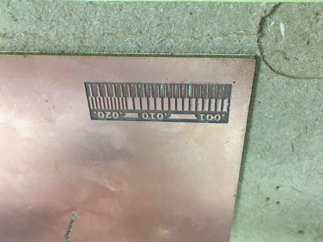
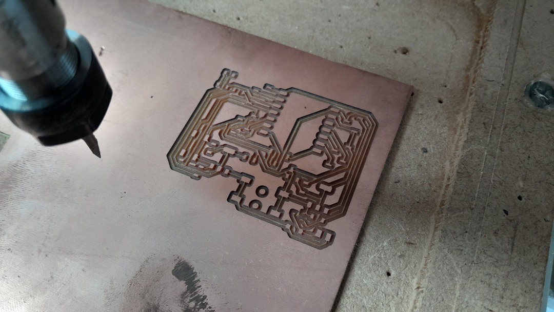
From the test I concluded that the machine can handle thin traces like 0.01 inch or 0.254mm.
Individual assignment
For my assignment I fabricated the same board I design in Week_6. I add a moseft, a voltage regulator and a powerjack to control a motor throughout two pins.
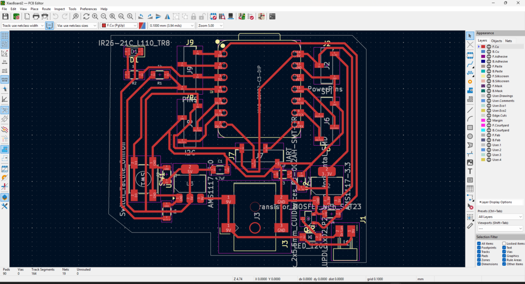
- For the design process I followed the same workflow with the designed parts.
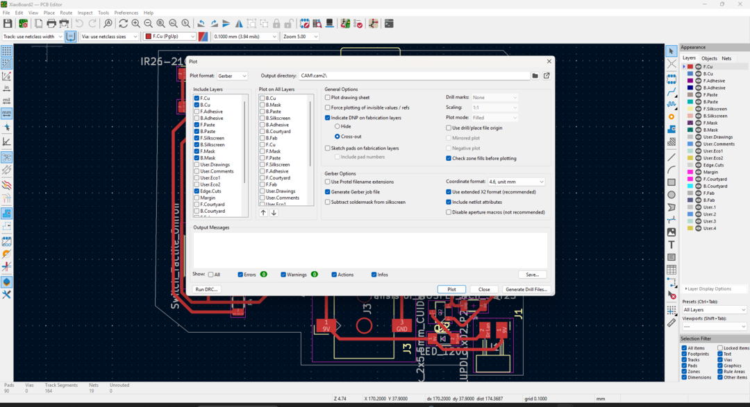
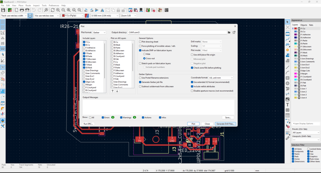
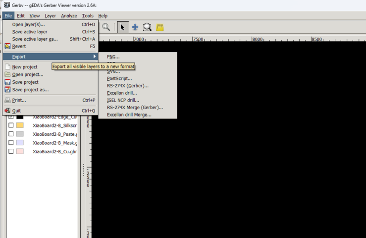
- Then I got the fabrication files including the drill files from Kicad.
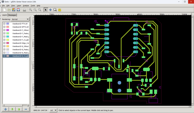
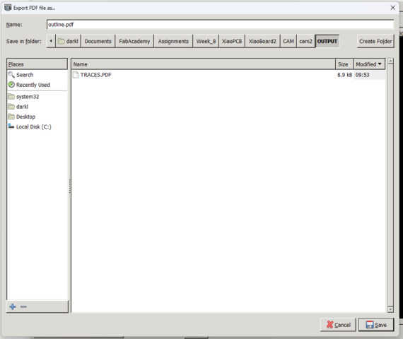
- Prepared the layers using gerbv to get the PDF files. for the Front, drills and outline layers.
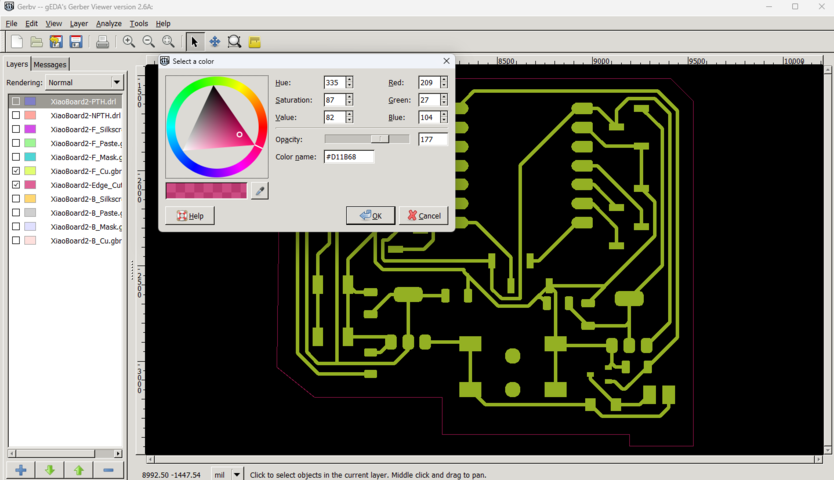
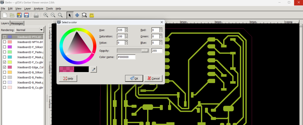
- I hide all the layers except the F_Cu and the Edge_Cut the change their color to black with 255 opacity.
- Then export them as PDF.
- I then repeated these steps with the drill file PTH.drl and the Edge_Cut but with hiding all the other layers.
- Then I did the same with the Edge_Cut only and hiding all the other layers.
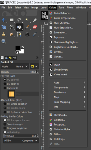
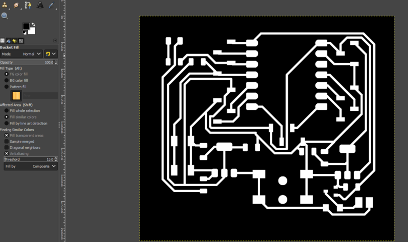
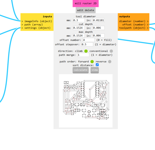
- Then used gimp to get png files for mods to get the gcode.
- In gimp When importing we must choose the resolution to be 1000pixels.
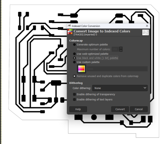
- After importing we go to Image menu -> Mode -> Indexed then choose Use black and White. This makes the image contains only dark and white pixels with no grayscaling inbetween. This step we do for all the PDFs.
- When we import the PDFs we see black and white lines and dots. We need to understand that the milling process will happen to the offset paths to the lines in white. To simplify we can say the the white space is copper to be left and the black areas is where the copper must be removed.
- For the traces we needed to invert the colors values we cand do the by going to Color menu then to Value invert.
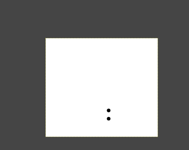
- We do the same for the drills without inverting because we need these black dot to be removed. and we turn the outline to white using the bucket tool.
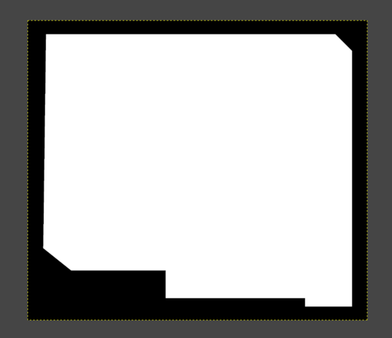
- As for the outline we fill the outer of the outline with black using the bucket tool.
- We export each of them as PNG.
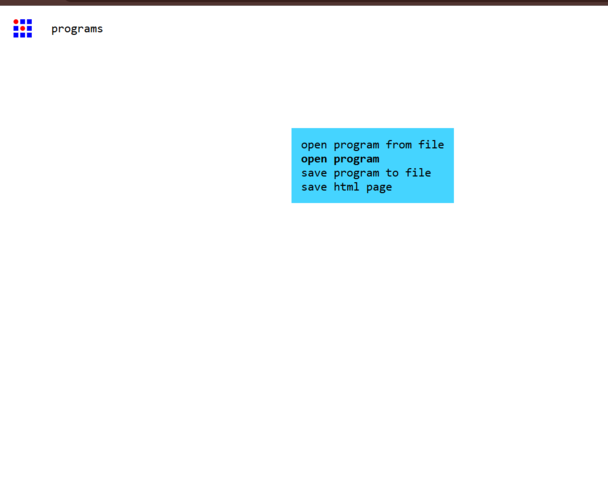
- We go to mods. right click to open the menu we choose open program.
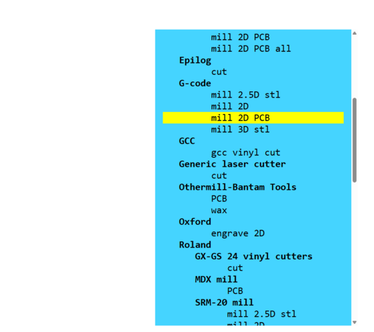
- Then go to gcode and then choose mill 2D PCB.
- Then I upload my traces.png file (of course we will repeat these steps for the other two files drills and the outline.)
- After uploading the traces we go to the mill raster 2D and enter the values for our bit and board setting. As you can see I used a 0.3mm endmill and the cut depth is just enough to remove the copper layer.
- Then hit calculate. The gcode file will be downloaded.
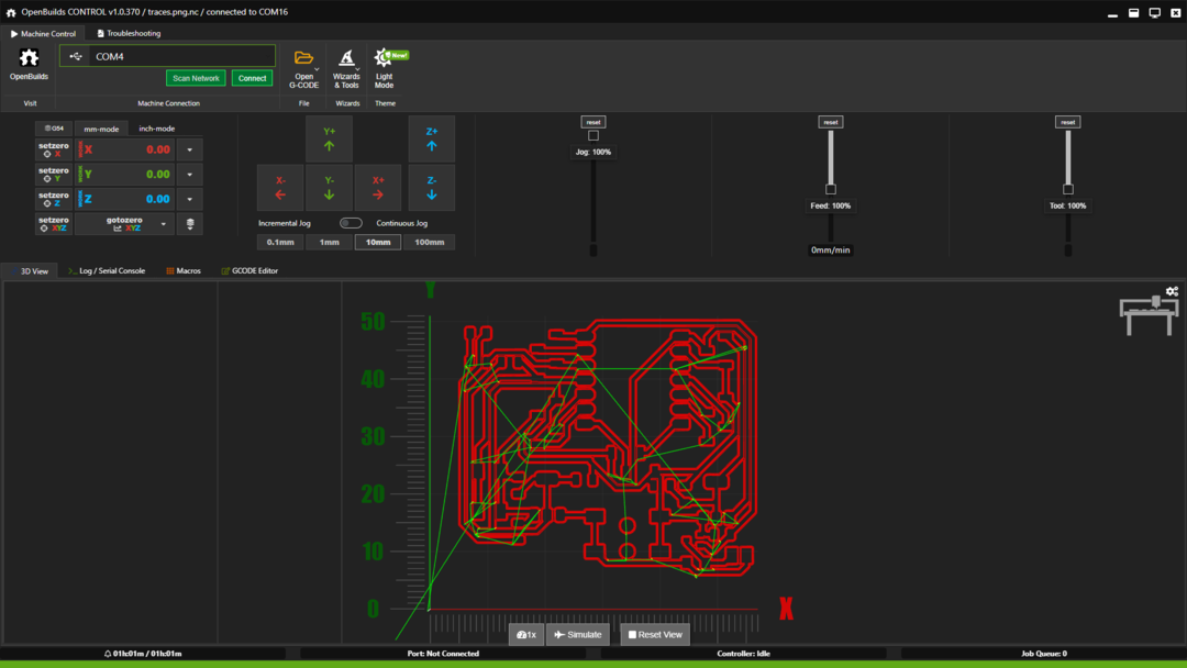
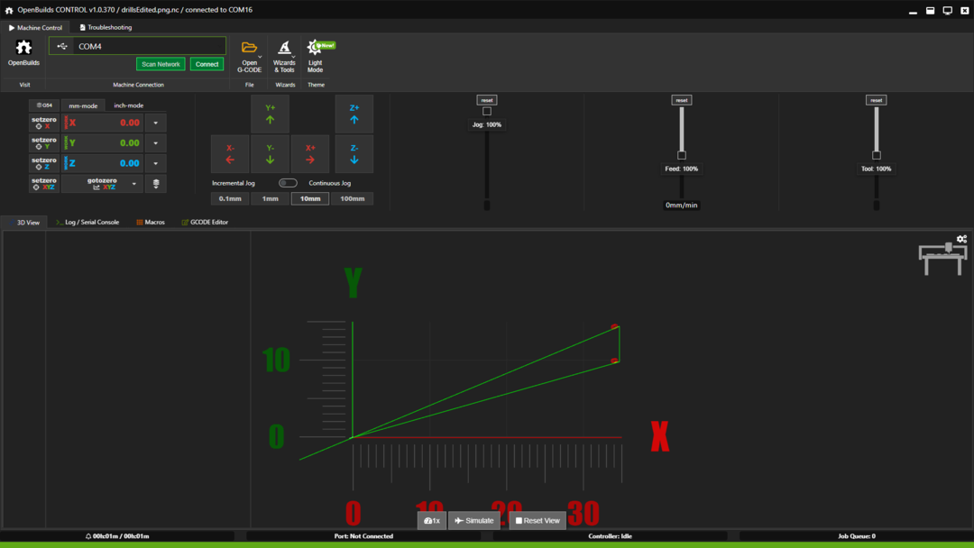
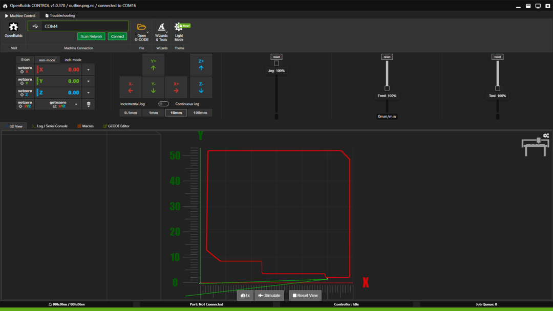
- I repeated the same steps for the drills and outines
- Now we move to Openbuilds to control the machine and upload the gcode for it.
- After setting the machine zeros in x and y axes. I turn on the spindle and lower the machine bit by bit until it touches the surface then set this as my Z zero point. We only need to set X and Y zeros once but the Z zero is different for each endmill and drill bit we use.
- After the milling I started soldering my board.
I added them to the schametaic.
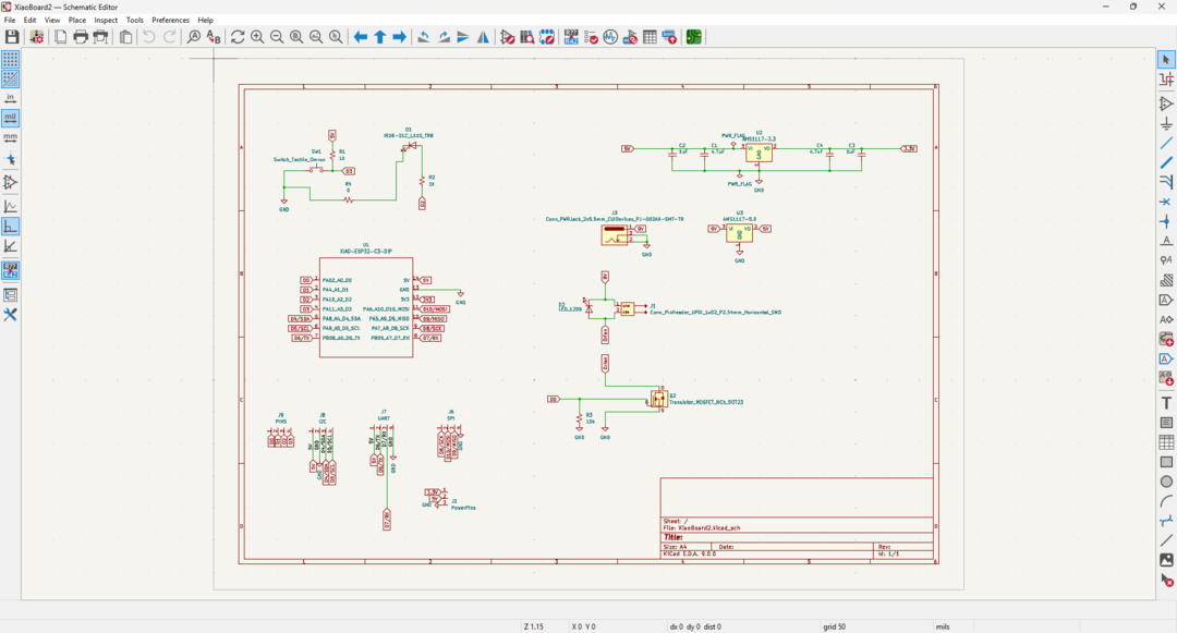
Then move to the PCB design.
You will notice the that outline is gone but its not I used the bucket tool to make it black so that it will be ignored and won't get milled.
After running all the process I got this final result.
Actually this was my third trial because in the first and the second one I was using a 0.3mm V-bit endmill but I accedintaly dug to deep into the board and the traces were too thin. This resulted in week traces and some were damaged.
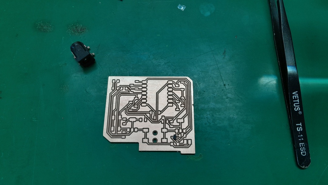
Final result:
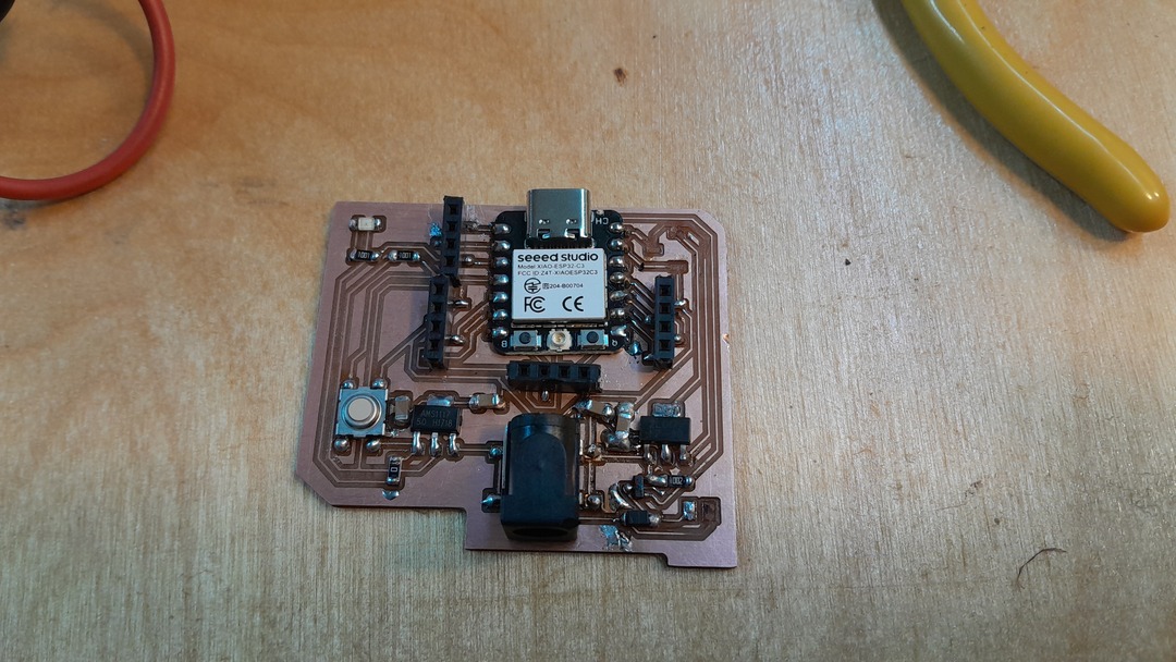
Testing the board and the on board input and output:
As you can see in the design I added a pushbutton connected to pin D3 in the Xiao ESP32 C3 board and connected to it a pull up resistor also I connected an LED and a resistor with pin D2 and an on board Input and output devices.
Code:
  void setup()
  {
    Serial.begin(115200);
    pinMode(D3, INPUT);
    pinMode(D2, OUTPUT);

  }

  void loop()
  {
    digitalWrite(D2, HIGH);
    Serial.println(digitalRead(D3));
    delay(1000);
  }