Week_6 Assignments
- Group assignment:
- Individual assignment
Our group assignment was to use electronics testing equipment like the multimeter, osciloscope and the logic analyzer.
I used KiCAD to design a PCB that acts like a dev board to the Xiao ESP 32.
Group assignment
As for the group assignment we learned how to use the oscilloscope to test the circuits and used arduino nano as a board to be tested.
It was a great experience to see how the PWM (Pulse Width Modulation) works seeing how the signal width changes.
We also used the logic analyser to see the serial data and decode it and see the result.
Using the oscilloscope is quite easy all we did to get the PWM signal is that we connected the CH1 connector to pin number 9 in the Arduino nano and the ground probe to the ground in the Arduino. Then uploaded a simple sketch to the arduino to send PWM signal to pin 9.
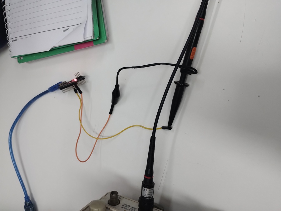
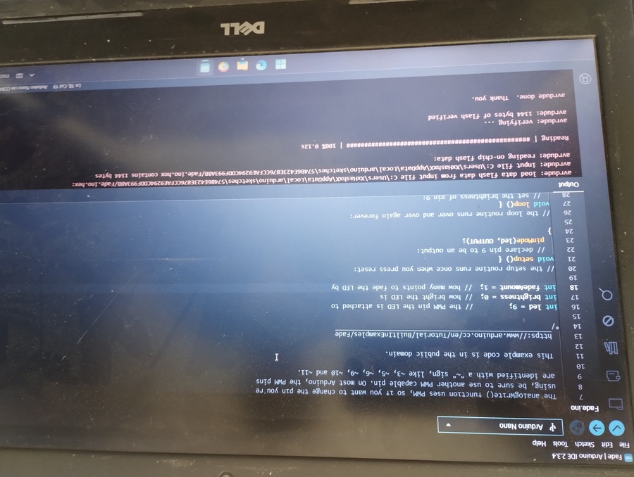
this was my first time using the oscilloscope and I plan to use it in the PCB fabrication week.
As for the logic analyzer we used it to decode the serial data interpreted to "Hello World". By sending this string data through the Serial.println() function and connecting the logic analyzer channels ti the TX and RX pins.
.jpg)
.jpg)
Individual assignment
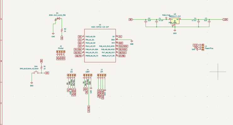
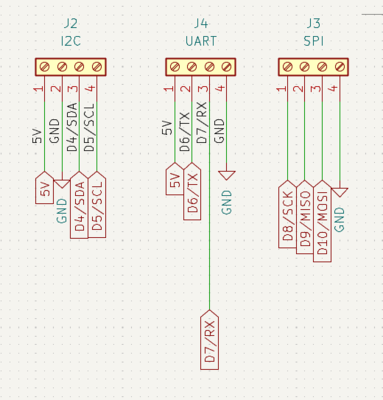
Like I said I used KiCAD to design the circiut I wanted to make a circiut that helps to connect the Xiao ESP 32 C3 to the prepherals whatever the protocol is whether it is I2C, SPI or UART.
I learned KiCAD following the documentation and the "Getting Started With KiCAD"tutorial provided by KiCAD.
KiCAD has a fixed workflow (I think ^^):
**I found that it is more efficient to run through these steps after adding each component.
- Design the circiut schematic.
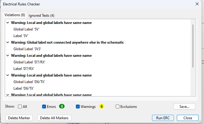
- Check the ERC "Electrical Rules Checker"
- Assign Footprints.
- Update the PCB layout from the schematic.
- UPDATE THE DESIGN RULES from File-> Board setup
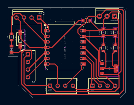
- Make the rounting (not an easy task ^^)
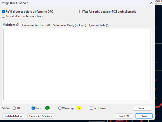
- Check the DRC "Design Rules Checker"
- Now you have it ^^.
Designing Steps
- Design the schematic. using the short key A to add symbols and W for wiring.
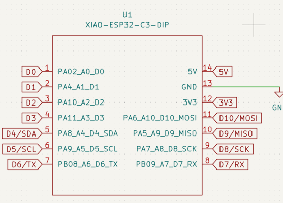
- I started by adding the Xiao-Esp32-C3 to the schematic and used the global label Icon to assign each pin name.
- I then added the voltage regulator circiut. The Xiao-Esp32-C3 has already a 3.3V regulator but I wanted to connect an extra one. I found it would be more challenging.
I searched for the pin out of the AMS1117 3.3V and I found this pic from EasyEDA.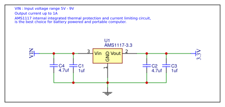
they added the capacitors to filter the noise whether it is coming from the input or the output. So I added this to the circiut.
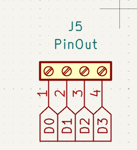
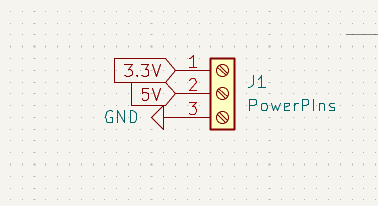
- I added Screw Terminal Blocks for the Power pins, GPIOs and the comminucation protocols.
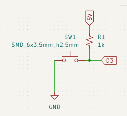
- I also added a push button that has a pull up resistor to act like an Input
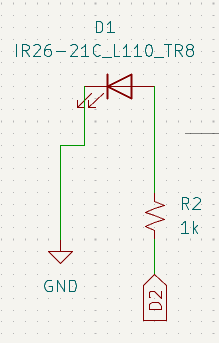
- I added an LED to act like an Output.
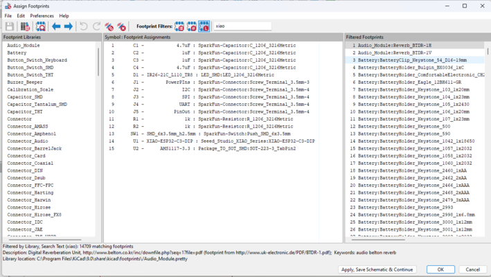
- After this I assigned each component a footprint using the Assign Footprint icon in the schematic layout
- After this I ran the ERC and finally I have no errors ^^.
- Next I went to the PCB degin layout and routed the PCB as I said it is much easier to go through the kicad workflow after adding each component.
- I updated the design Rules to fit my machine and the bits that is available with me.
- Then I started routing the PCB traces.
- Once I am happy with the routing and all is connected I ran the DRC and the errors is not to be found ^^.
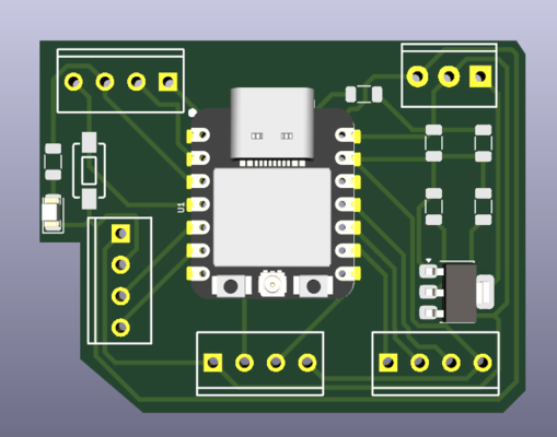
- KiCad has an awesome feature that lets you add capture the 3D design of the board.
- I exported the file in step extension to design a casing using fusion 360.
