6. Electronics Design
Overview
This week I learned how to design a PCB board in KiCAD and milled it for my individual work. For my group work I tested a XIAO RP2040 with a oscilloscope and a analog discovery 2.
Group Work
This week we were asked to test a microcontroller using diffrent hardware testing devices. The ones we used were a multimeter, a oscilloscope, and a analog discovery 2. We used these tools to measure the voltage flow in a fading LED that was hooked to an XIAO RP2040. First with the multimeter we saw the change in number form. With the Ociloscope when the alligator clips were put onto the two ends of the LED, we saw the change in the form of 2 lines, one represented low and the other high. The line that was low would get bigger when the LED went low and would get smaller when the LED went bright. It was opposite for the other line which represented the HIGH part of an LED. Finally with the Analog Discovery 2, we used pinheader wires on the same track as the LED to get jagged waves the represented the LEDs rise and fall in brightness.
What is Electroinc Design Automation
Electronic Design Automation (EDA) is a type of software used to help engineers design and build electronic circuits, such as microchips and circuit boards. These tools make the process faster and more accurate by allowing engineers to create, test, and improve their designs before they are built.
Some important parts of EDA include:
-
Schematic Design: Engineers use software to draw circuits and connect components.
-
Simulation: The design is tested in a virtual environment to make sure it works correctly.
-
Synthesis: The circuit design is turned into a format that can be built, like a blueprint.
-
Layout and Routing: The physical design of the circuit is created, arranging components in a way that makes them work efficiently.
-
Testing: The final design is checked for errors before it is manufactured.
EDA is important because modern electronics, like computers and smartphones, are extremely complex. Without these tools, designing and building advanced technology would take much longer and be more difficult.
Designing a Board
Lookback
I first thought of what I was going to design in KiCAD. I landed on making my pull down resistor LED design I used for my embedded programming week.
Seting up KiCAD
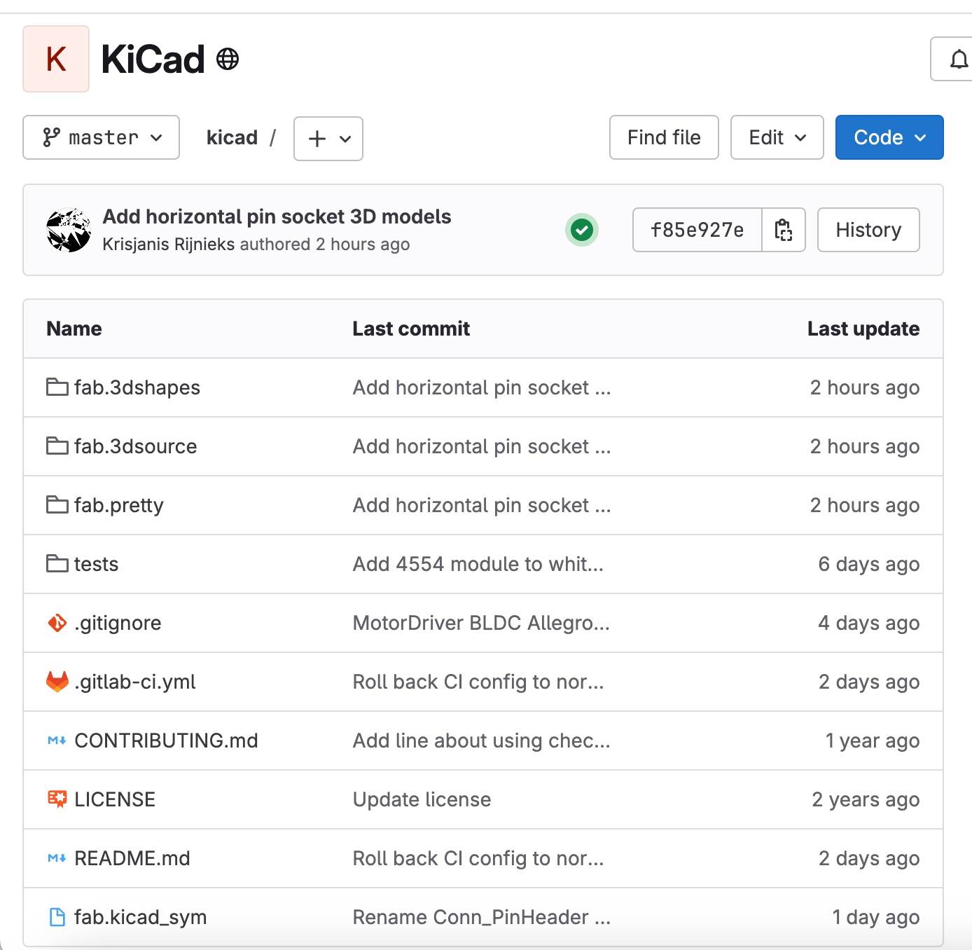
I first went to the KiCAD website and downloaded the version for Mac. Then to get to the libraries that we use for Fab I first went under the assignment for the week and opened the link to the libraries. This led me to a Git website with multiple options for libraries for different PCB board designing softwares such as Eagle and KiCAD. Under the KiCAD file I followed the instructions:
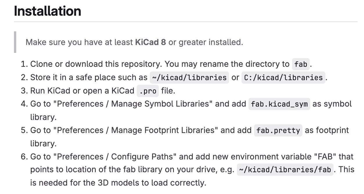
Adding Componets
To understand how to use KiCAD I followed this Tutorial and learned how to make PCBs. I had used KiCAD in the past and it is the only board designing software I used during the week. To setup the PCB I first had to have all the components needed and what they were connected to. To do this I made a new project and opened schematic editor. To add components I clicked on the symbol button and added the following components: 1 XIAO RP2040, 1 Surface Mount Button, 1 Surface Mount Light Emiting Diode, and 2 Resistors (The value doesn’t matter since it is added after the board). After I had all my components in the editor, I added wires going from component to component based off my design I made on the breadboard for embedded programming with a few diffrences since a PCB is pretty different from a breadboard.


Component and wire tools
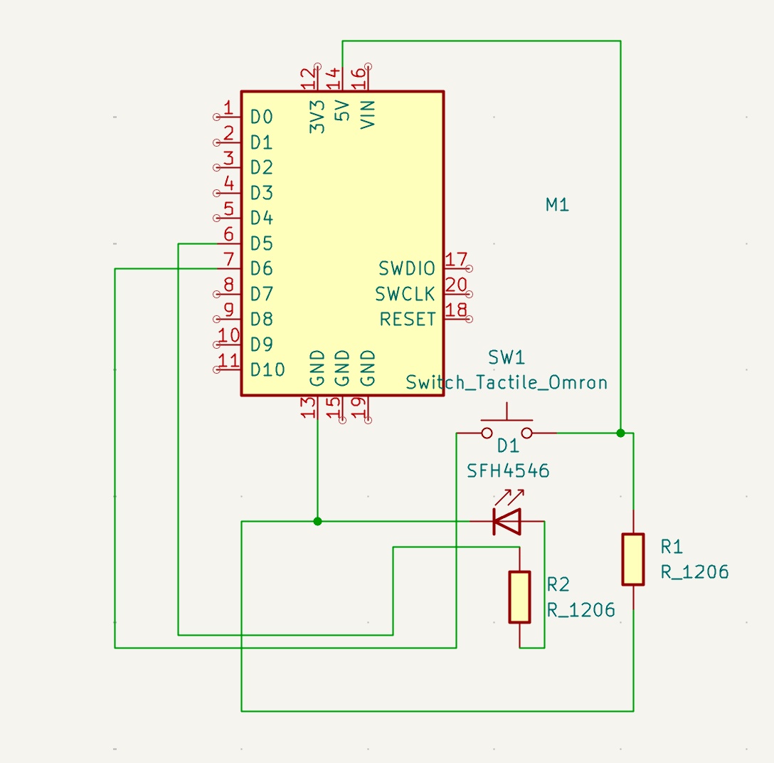
Here iss my completed schematic design. You can see the wires each go from place to place for their respective component. The button was a bit strange since it has 4 nodes in design but only 2 in schematic mode, but after checking it in the PCB editor, I learned that as long as the correlation of the wires were correct (where the signals were to go to) then it didn’t matter that I had two wires going into the same port in the schematic editor
Mapping them out
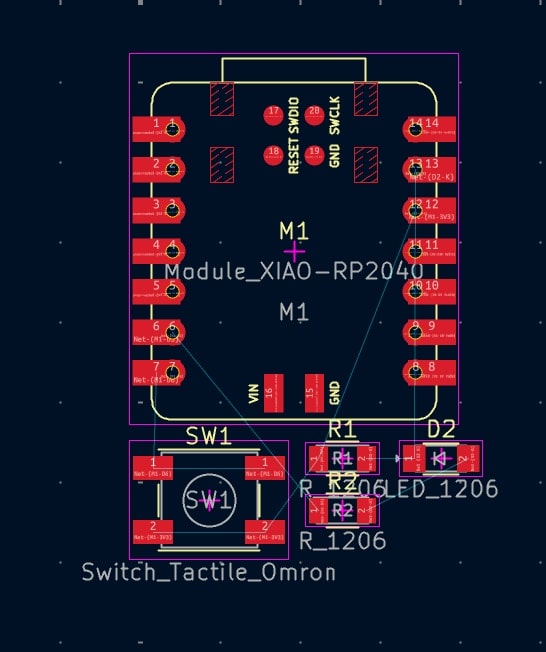
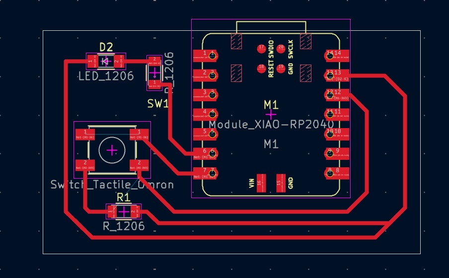
The PCB editor is where the real work comes in for KiCAD. To start when you open it you first needed to press the update button to bring all the components and connections from schematic editor to PCB editor. Once that’s done I had to set up the components in a way where the wires wouldn’t overlap one another since it wouldn’t work if they did. This was completed through a very intricate process known as guess and check. I would place the components in a way and run wires to all the diffrent components. Eventually I would run into a problem and would need to move around components. I did this several times and eventually got my wires to work. From there I changed my line type from an F cut to an edge cut. From there I made a box almost encapsulating all the componets except the RP2040 so that it would be easier to plug in the USB-C plug. It is a process that tests the patience of the individual.
Milling
Installing bit and PCB Board
First thing I had to do when using the CNC machine is install the drill bit. I assumed I’d be using the 1/32 bit for most if not all of my custom PCB so I installed that one. To do it I first had to remove the drill but that was currently in the CNC Machine to learn how to switch them out. To do this I used two wrenches, one right above the drill to unscrew it and one high up to hold the drill in place. After the old bit was removed I added the new bit into the hole and manually screwed it in until I needed the wrench. From there I used the wrenches again but this time to tighten the bit into place. For the PCB board I found one that could fit into the machine in the Fab Lab and put double sided tape on the non-copper side.
Setting up file
I first exported my files using the plot feature. I only grabbed the files for edge and F cuts since they were the only types of cuts I designed for my board. From there I sent the files to the Milling Machine. It gave me a third file known as the job file when I plotted it, I didn’t need it for milling but it’s in my files regardless. On the Bantam Software I added both files (F and edge cuts) and finsihed prep.
Milling
Cleanup and soldering
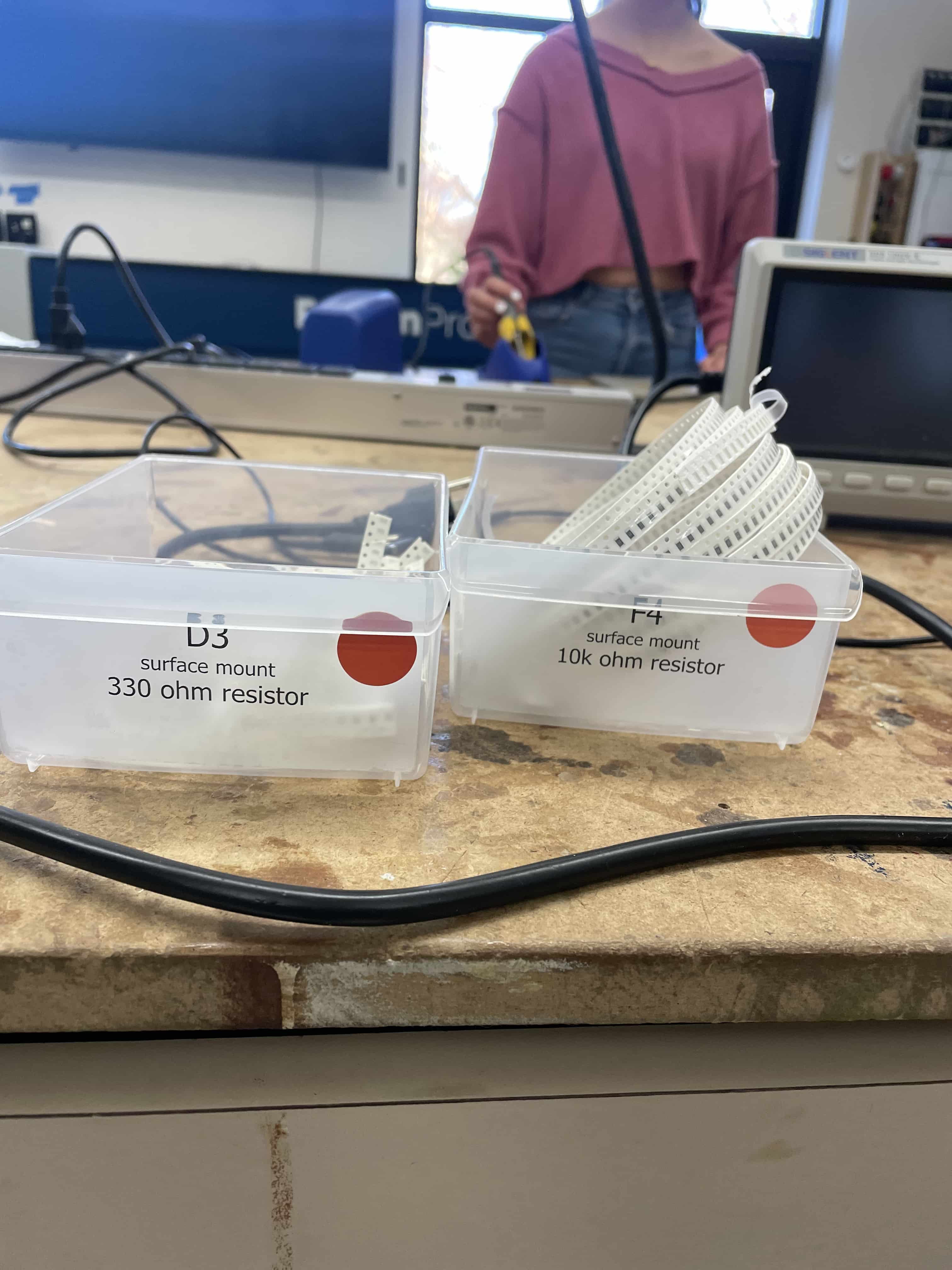
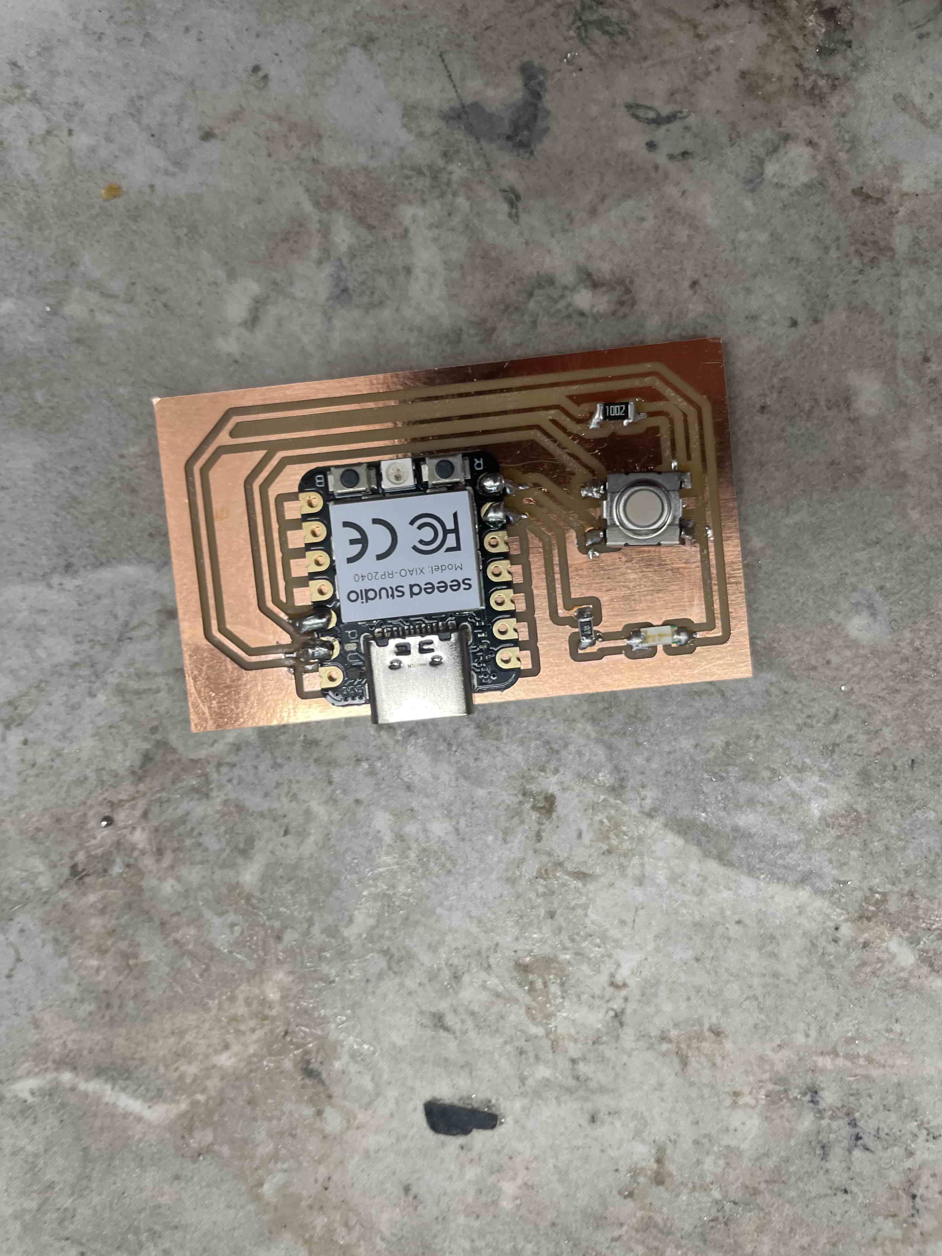
After the milling was completed I cleaned up the the excess pcb from the drilling with a shop vac and removed the PCB. Afterwards I found the right resitors, an LED, a button, and a RP2040 for the board. After a bit of struggle soldering because surface mount is tricky I had a working example of my PCB design.
Reflection
This week was a bit tricky since KiCAD is very different from something like Wokwi so there were a few challenges faced during the week. Mainly in deisgn the PCB Board without having the wires overlap. I learned how to add libraries to KiCAD and I thought that was very cool since it allows me to download other libiraries for unique componets in the future. Overall it was an enjoyable week.