Electronics Production
This weeks individual assignment:
- make and test a microcontroller development board that you designed
This weeks learnings:
This week, I learned that I'm already getting along surprisingly well with KiCad, and that milling circuit boards is also going well. The workflow as it's done in Bottrop isn't quite right for me yet, so I hope to use the coming weeks to delve deeper into it. This also applies to the soldering workflow, but it worked out for this week nonetheless. Enjoy looking through it.
PCB Design
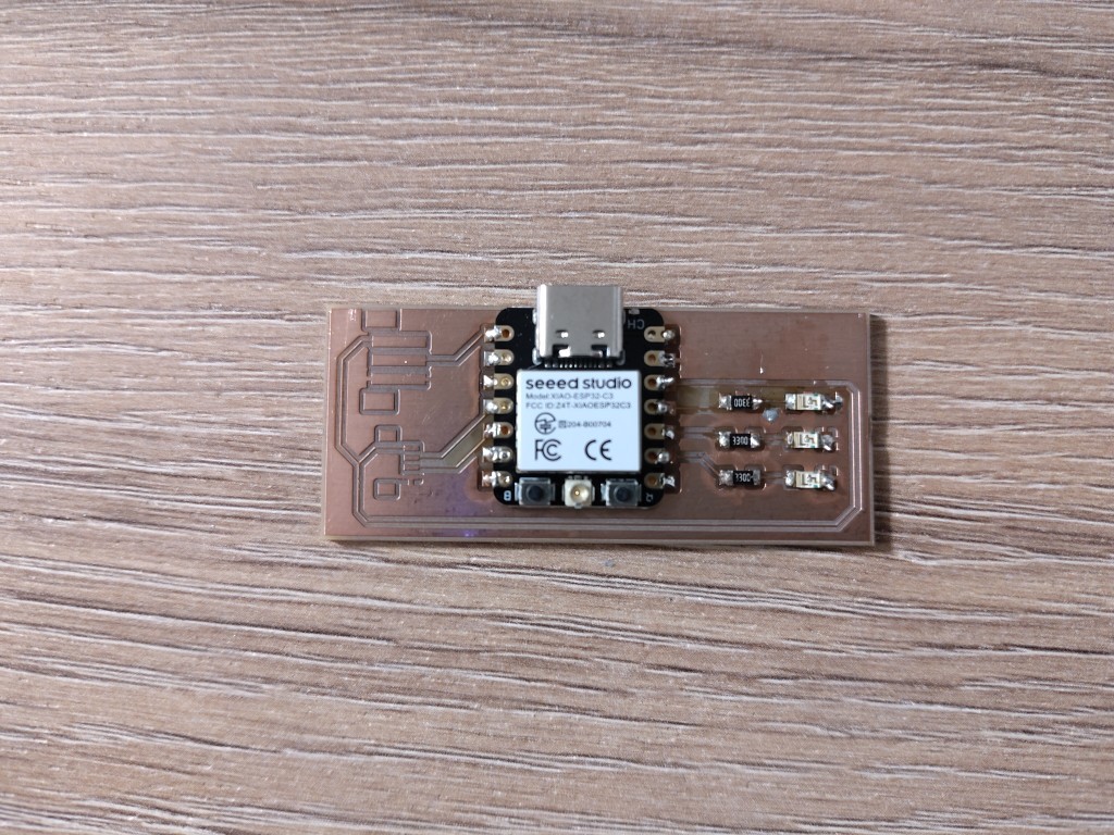
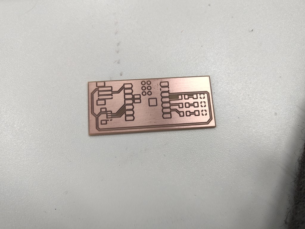
The week began with the kind of news you'd expect. The parts needed to work with the PCB from week 6 arrived on Wednesday. Unfortunately, that was exactly a week too late to do anything with them. So, I quickly and dirty-built a new board with three LEDs, each with 330 ohm resistors, and two JST sockets for one three-pin and one four-pin connectors. The JST sockets will allow me to make wired connections to my sensors and actuators in the coming weeks, as well as for experiments during my finals. I don't need them this week—but I can't solder them yet due to a lack of materials.How to work with KiCad is described in week 6, so I'll just show my schematics and my board here.
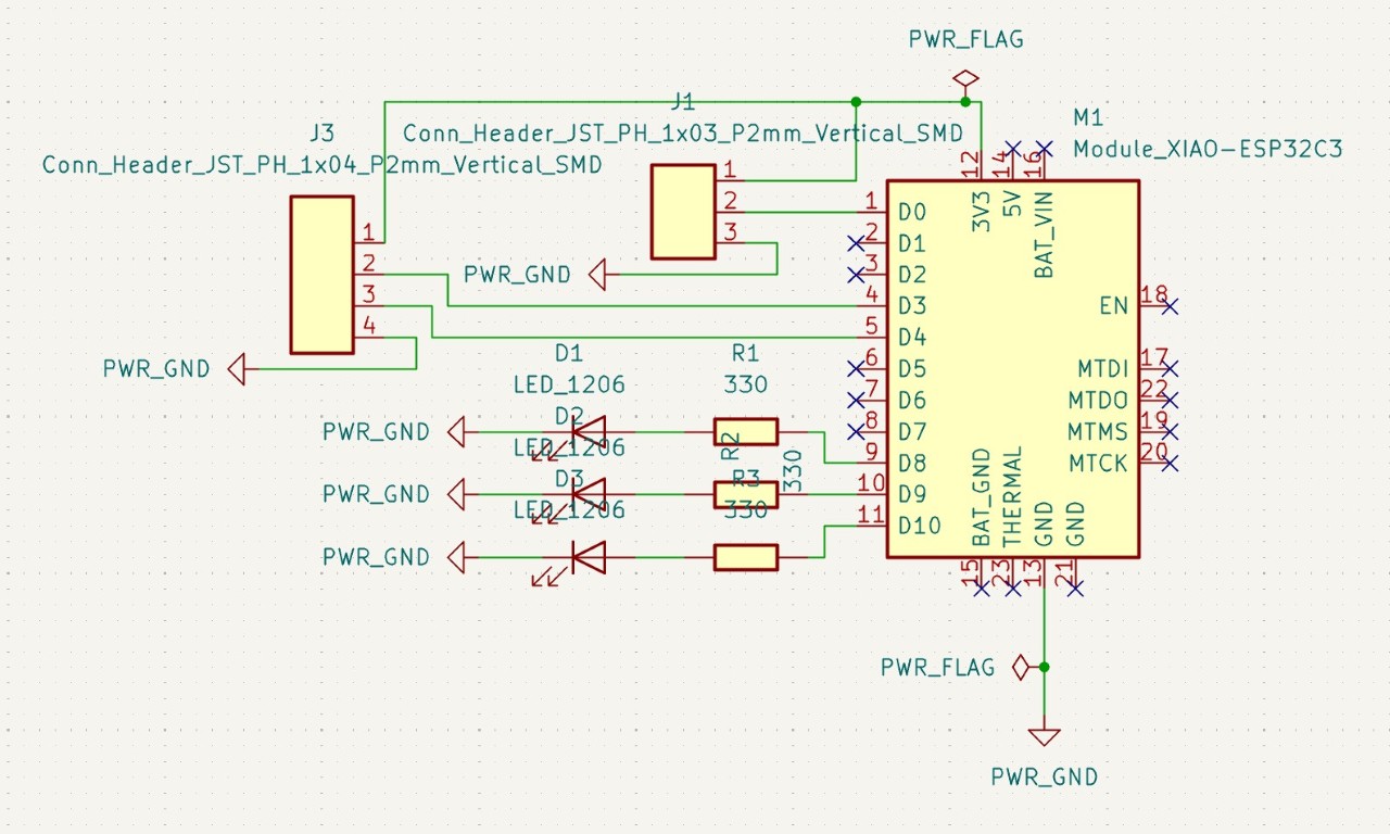
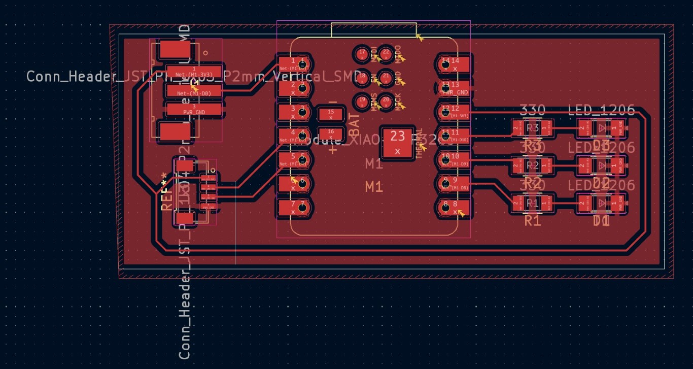
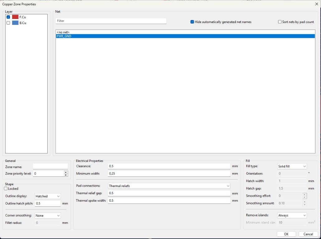
Perhaps you can think of a change compared to the approach in my last KiCad design: I'm now working with the ground plate, using the entire surface of the PCB as the ground. This saves me having to connect each ground with a wire, and therefore removes more material overall, thus also preserving the milling cutters. The whole thing is incredibly easy to implement if you select "Draw Filled Zones" in the right-hand menu bar and then click to place a first point outside your board. This opens the following menu, where you select PWR_GND, as I did.
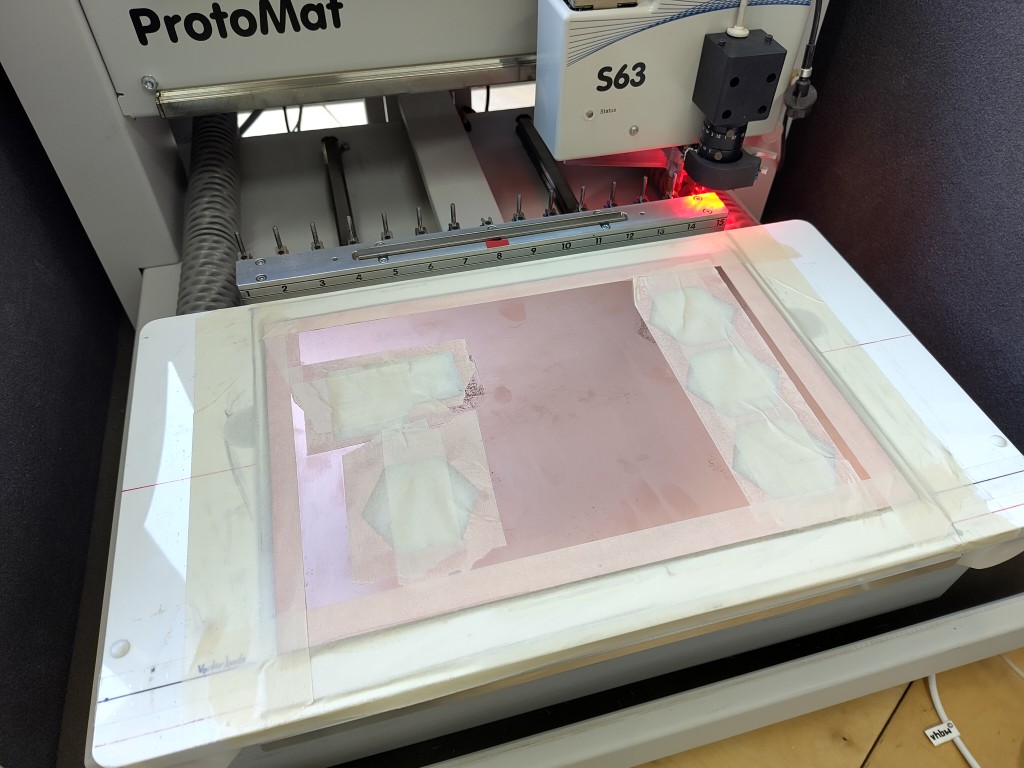
Milling
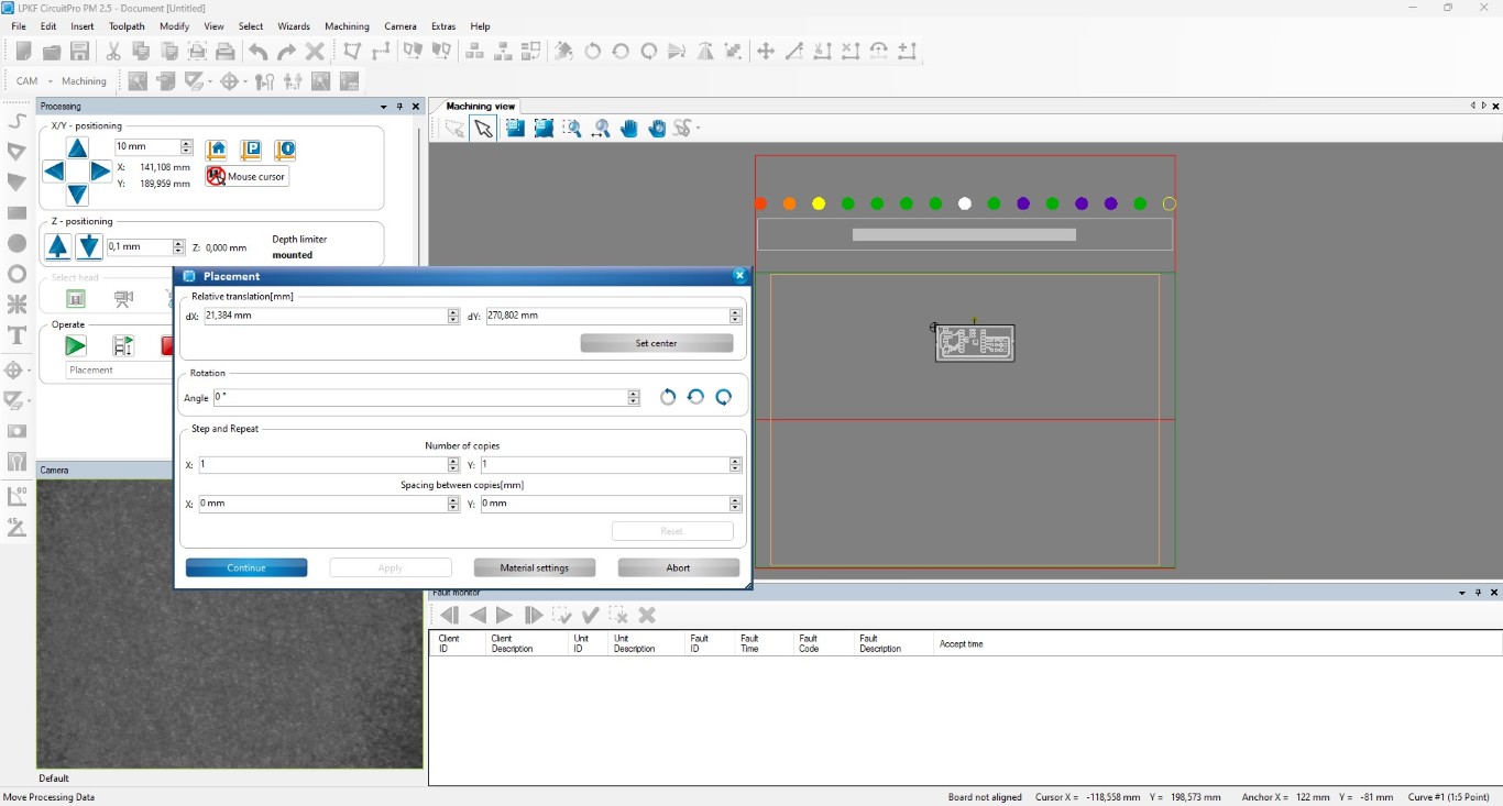
Next, we moved on to the milling machine itself, or rather, the associated laptop with the program. The HRW FabLab houses the LPKF Protomat S63, and the associated software is LPKF Circuit Pro. It seems important with this machine that it be turned on before opening the associated program on the laptop. Only then will the machine be automatically detected, and the corresponding dialog will appear when the software is opened.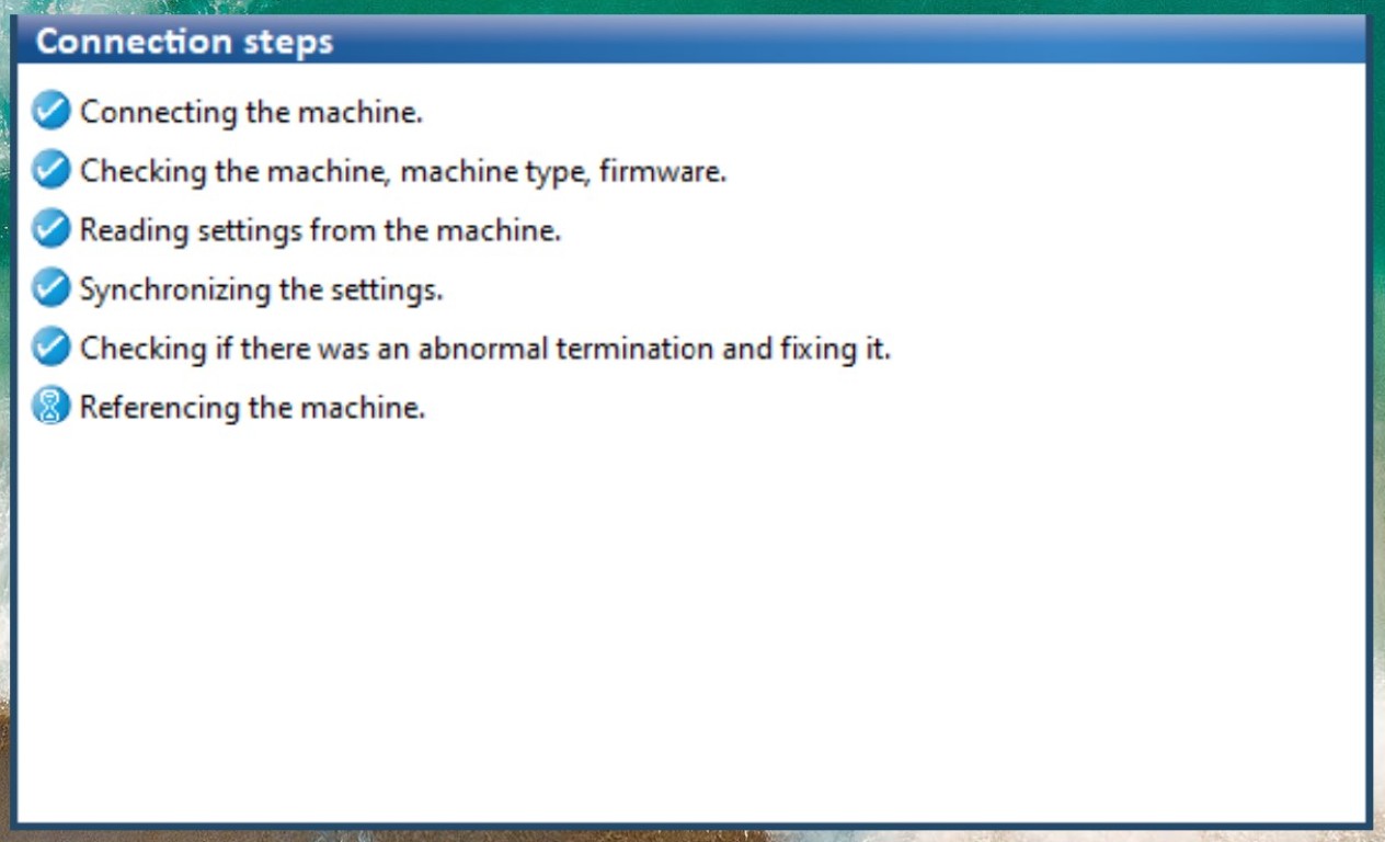
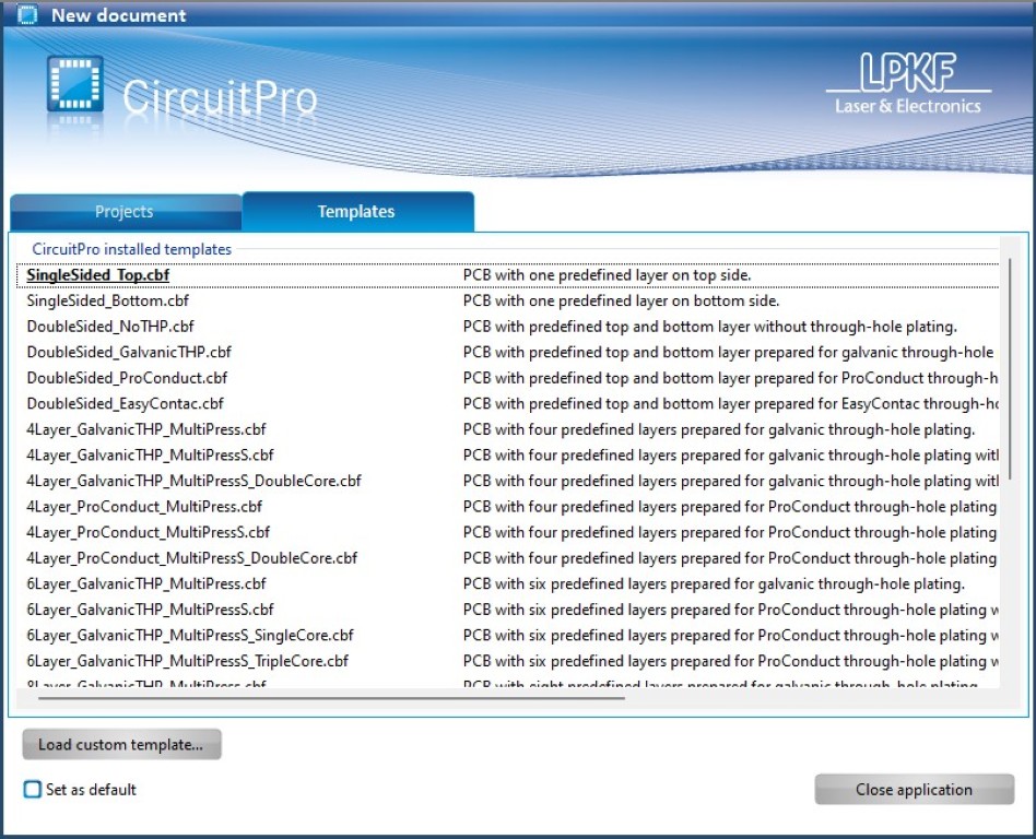
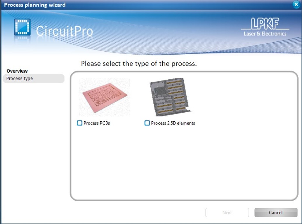
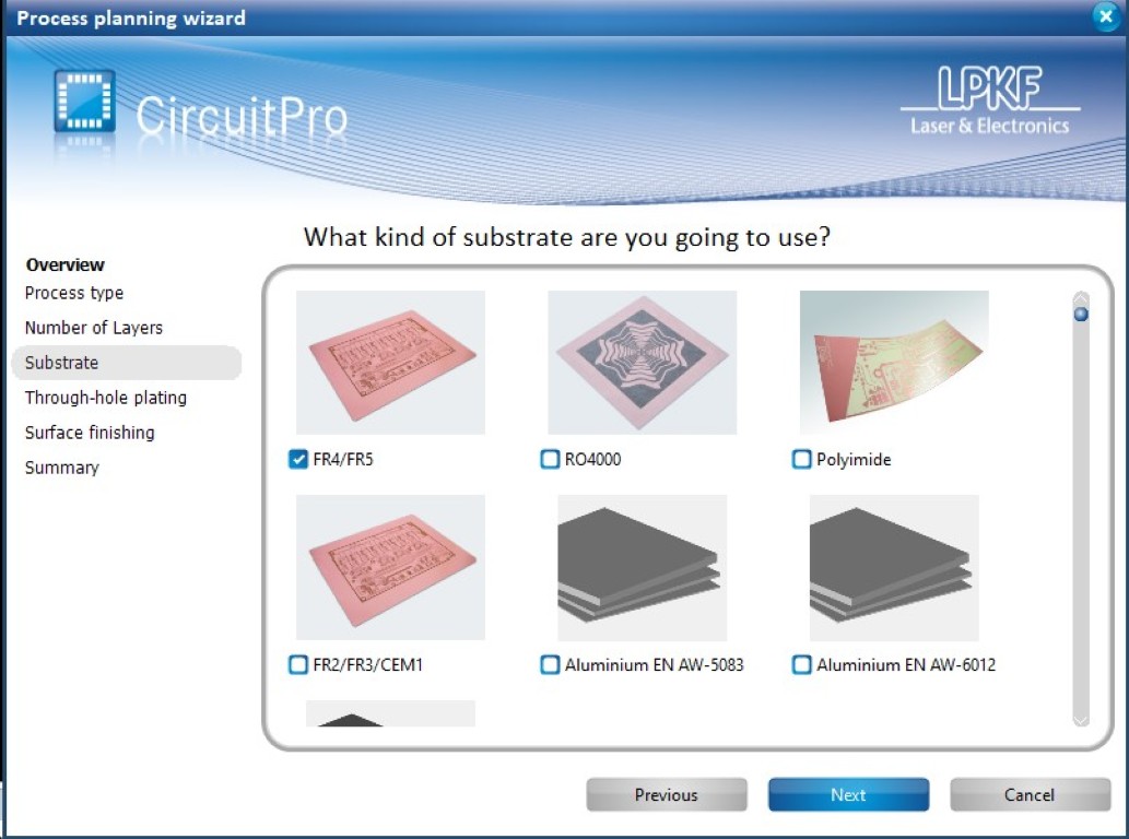
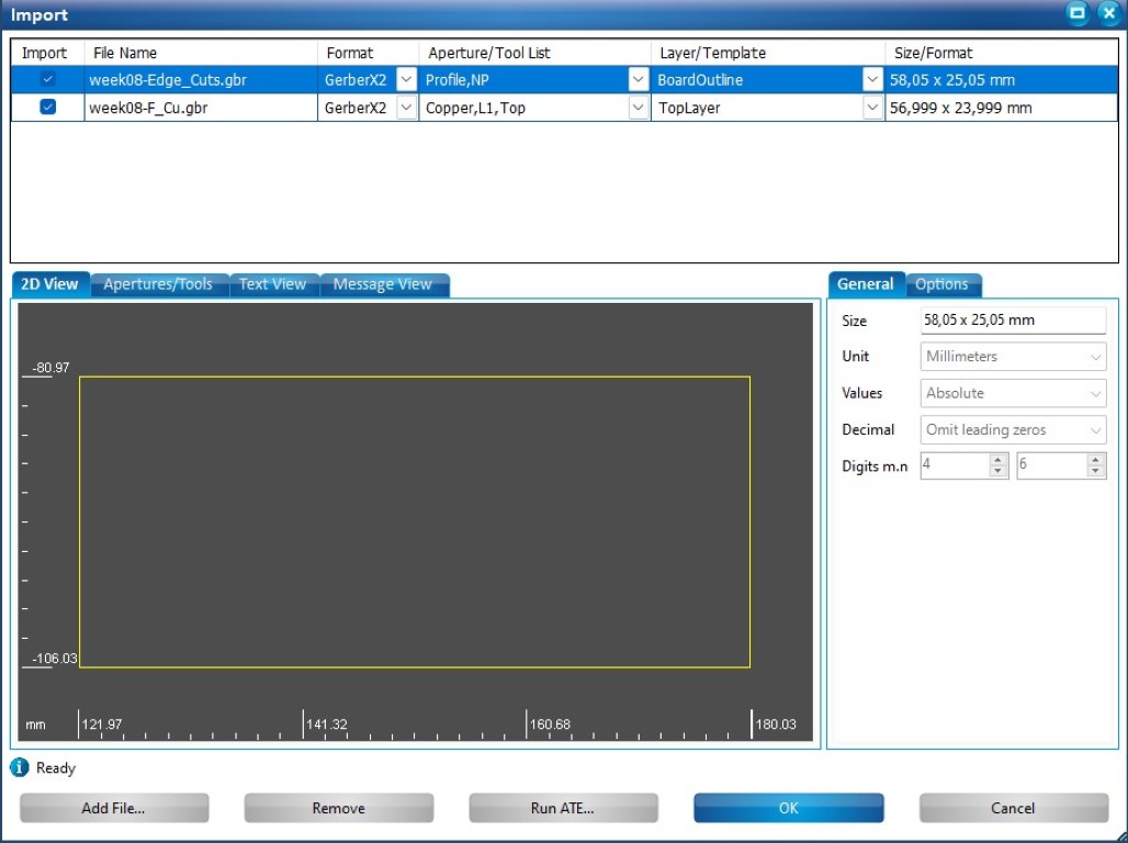
Next, we move to the right in the menu and import files into our project—namely, the two .gbr files for the top layer and the edge cut from KiCad. Next, we'll be asked to assign the imports, and the software will attempt to assign the layers automatically. In my case, the automatic assignment was correct, but this wasn't always the case for my colleagues, so you should check here to see if this is the case.
1 / 4
2 / 4
3 / 4
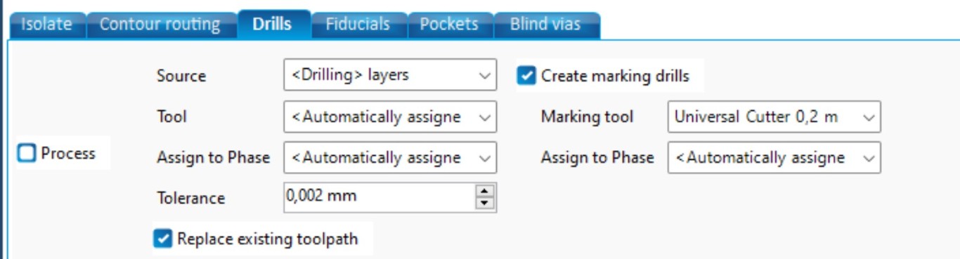
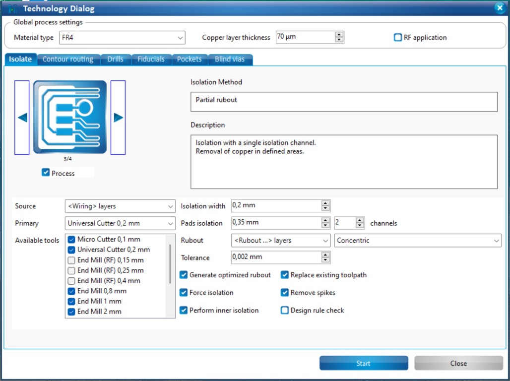
Here and in the following menus I have deselected the process because I don't need drills, fiducials, pockets or blind vias.
4 / 4
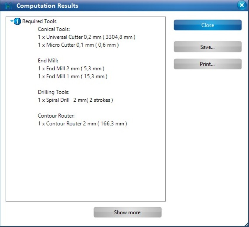
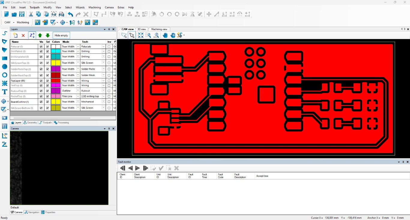
Once the menu is closed, you will get a list of tools, similar to this one.
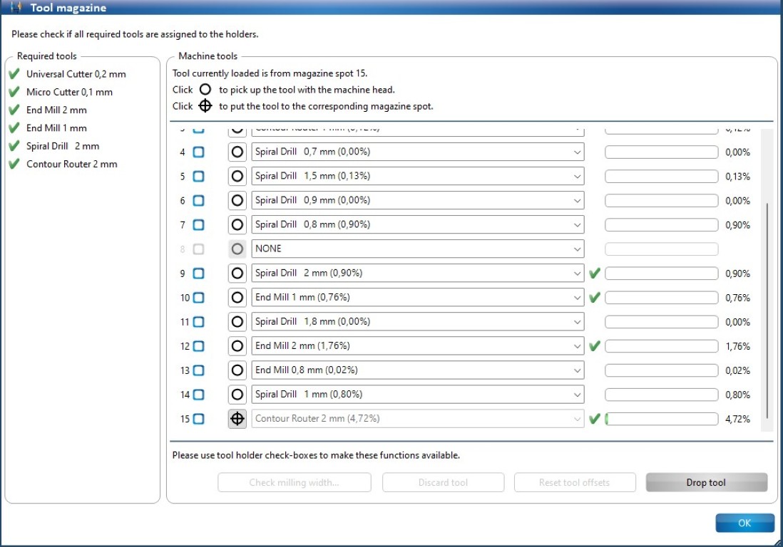
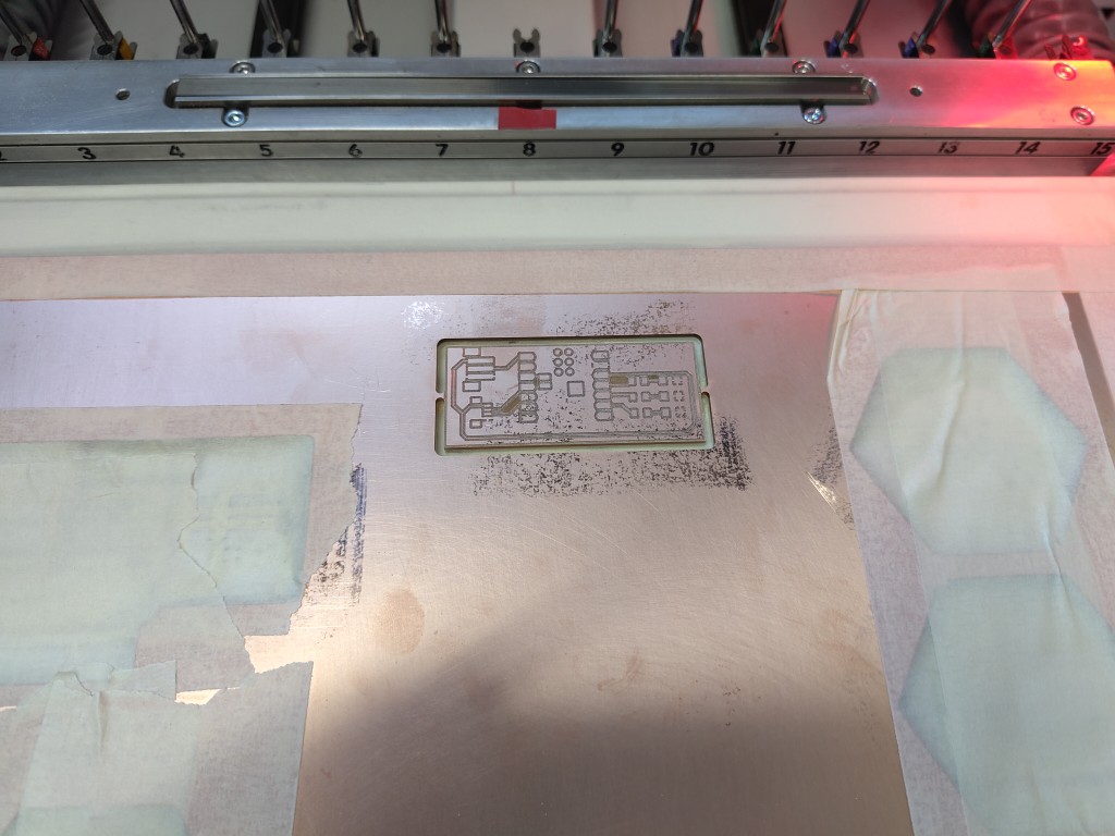
After all that, you should check the drill bits and see if they match the drill bits actually stored in the respective positions in the machine. That wasn't the case for me, so the check was definitely worth it.

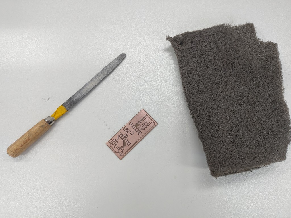
Measuring and soldering
The first thing I did afterward to inspect my circuit board was to put it under a 3D microscope to check for any copper particles I might have ground into the insulation tracks. So, I looked at all the tracks. While that may sound tedious, it took a maximum of five minutes. This is roughly what the image the microscope provided us looks like.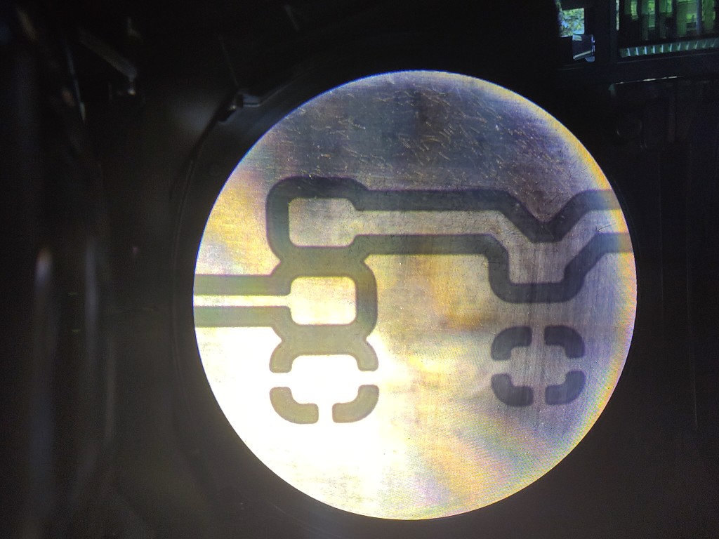
1 / 3
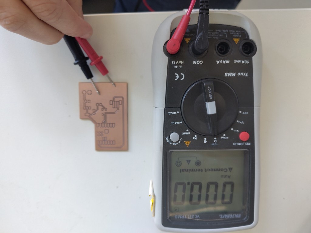
for connected parts, the resistance should be 0 or close to 0.
2 / 3
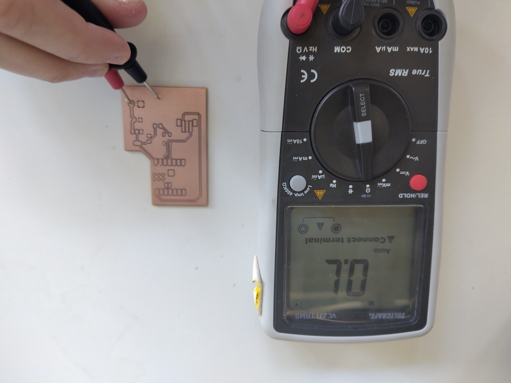
supply and/or data lines should not be connected to the ground plate, otherwise a short circuit would occur
3 / 3
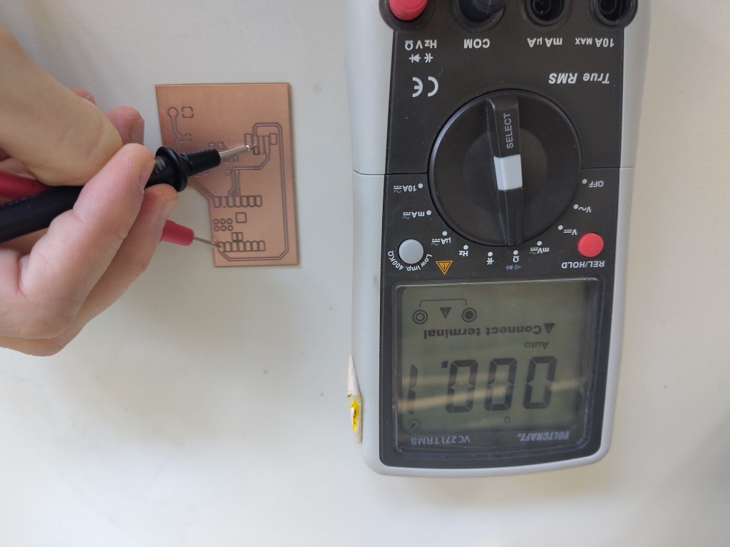
I also measured the beginning and end of the trace; here the resistance should again be 0 or close to 0
After that, it was time to solder my components. As already mentioned, this week's work was still very manageable. To get a better grasp of soldering on the circuit board, I made a few solder joints on an old piece of leftover material, which definitely helped me.
As a result, I preheated the solder joints with the soldering iron for a little longer than usual, probably between two and three seconds. After that, everything was basically as usual – for me, soldering went relatively well. However, I noticed that this isn't always the case with the others. Nevertheless, my circuit board will not win any beauty prizes in this lifetime, but as they say in Germany: It could be worse. Perhaps the best part is that I won't have to spend any time at art exhibitions using my soldering skills anytime soon, so I can continue to focus fully on FabAcademy.
1 / 3
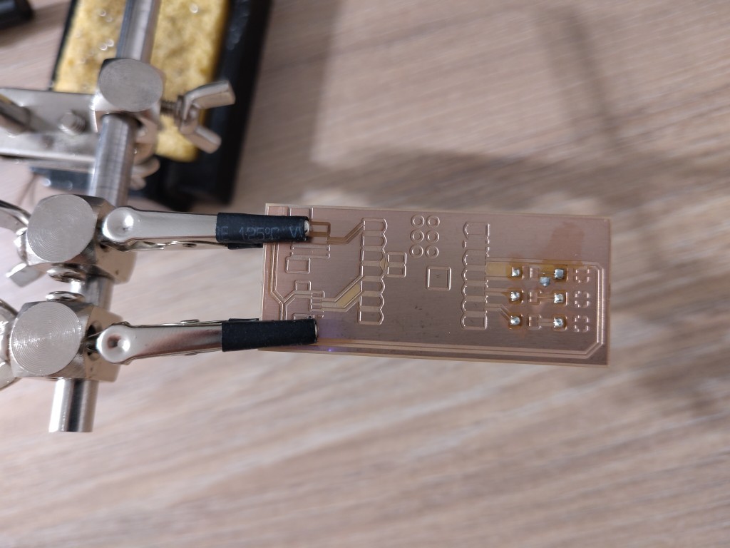
first, I made a spot of solder for each component, which I then melted again with the soldering iron, in order to push the component into the liquid solder with tweezers
2 / 3
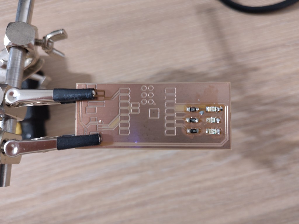
this is what it looked like after adding the resistors and LEDs. After each step, I checked the connections with a multimeter.
3 / 3
I also pushed the microcontroller into a soldering point first and then worked on all the other soldering points
Testing
To test my PCB, I wrote the following very simple program that turns one LED off every half second and then turns them all back on together.
int led1 =8, led2=9, led3=10;

void setup() {

	pinMode(led1, OUTPUT);
	pinMode(led2, OUTPUT);
	pinMode(led3, OUTPUT);
}

void loop() {
	digitalWrite(led1, HIGH);
	digitalWrite(led2, HIGH);
	digitalWrite(led3, HIGH);
	delay(500);
	digitalWrite(led1, LOW);
	delay(500);
	digitalWrite(led2, LOW);
	delay(500);
	digitalWrite(led3, LOW);
	delay(500);
}
Looking at the video, you'll see that the whole thing works wonderfully despite its high complexity. That wasn't always the case; during my first upload, only two of the three LEDs worked, which prompted me to re-test that exact wire. There were no errors, so I looked back and forth between the code and the circuit. I noticed that I had assigned the outputs to pins 9 to 11, but pins 8 to 10 were actually wired. With this correction, everything worked perfectly. Lesson learned: Even if the circuit is long forgotten by this point, don't lose sight of it if you notice errors.
Thats it for this week. Keep your fingers crossed that the Digikey order arrives promptly – then week 9 will continue tomorrow.