This weeks individual assignment:
- use an EDA tool to design a development board that uses parts from the inventory to interact and communicate with an embedded microcontroller
This weeks learnings:
Although I am familiar with current and voltage and everything else that goes with it, the standards this week were significantly different to what I am used to. I have come
to the conclusion that I find it easier in larger dimensions and unfortunately I have not yet been able to develop any overwhelming anticipation of making this week's PCB
myself in the near future. I've made just about every mistake you can make when it comes to design, so I'm happy to serve as a bad example this week. At least for my personal
learning curve, I think that was just as good. I have rarely worked with an oscilloscope before, but that was for me just a matter of getting used to the device - in the future
I may use it more often.
Designing a development board
This week's journey starts for me with the KiCad program, which has just been released in version 9.0.
KiCad is an EDA tool that we can use to design the development board for this week.I started by downloading the KiCad library from FabAcademy from GitLab and implementing it
according to the README document that is also stored there.
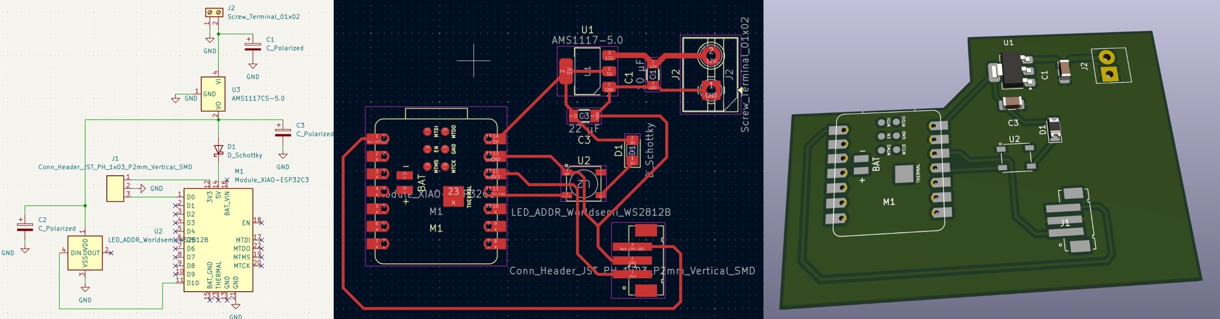
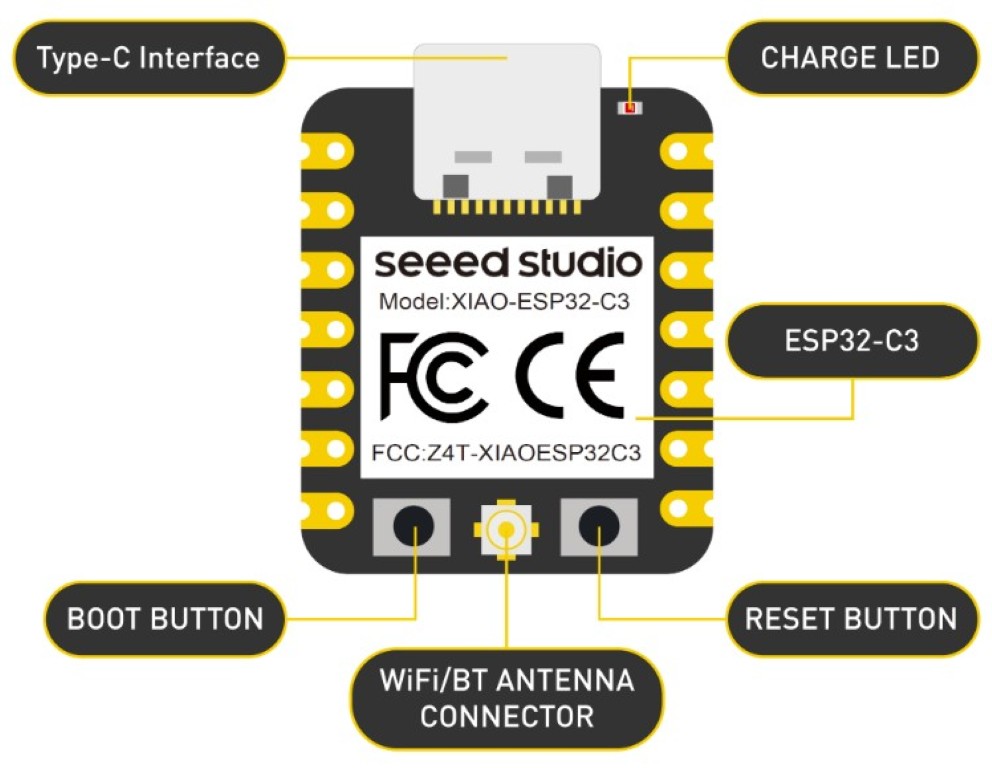
If you have been following my last few weeks, you will know that I want to use the ESP32C3 for my final project. Since this is my first board, I am working with a pre-made board from Seed Studio
to simplify things this week and probably in the coming weeks, namely this one: Seeed Studio XIAO ESP32C3.
Accordingly, I will build my development board around this this week.
As you can see in the picture, reset and bootloader buttons are already installed on the board. In addition, an LED is soldered on as a status indicator, which would otherwise
also have had to be placed on my development board. Everything else we consider in the design is based on the desired functionality. Since a USB-C port is already soldered on, we don't have
to worry about flashing or the power supply.
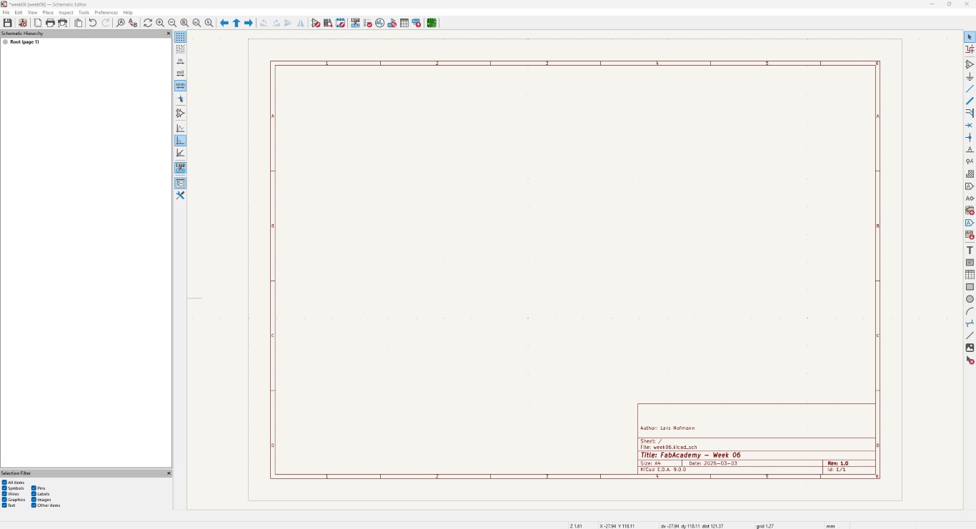
But now let's turn our attention to KiCad: After installation, we create a new project and open the schematics or .sch file. We will carry out the first editing steps in this.
In the first step, I adjusted the description in the bottom right corner and entered my data there so that I would still know what I was dealing with in a few weeks. This is very
easy to do at the top left via File > Page Settings and then the relevant entries. The result of this step can be found in the lower right corner of the following image.
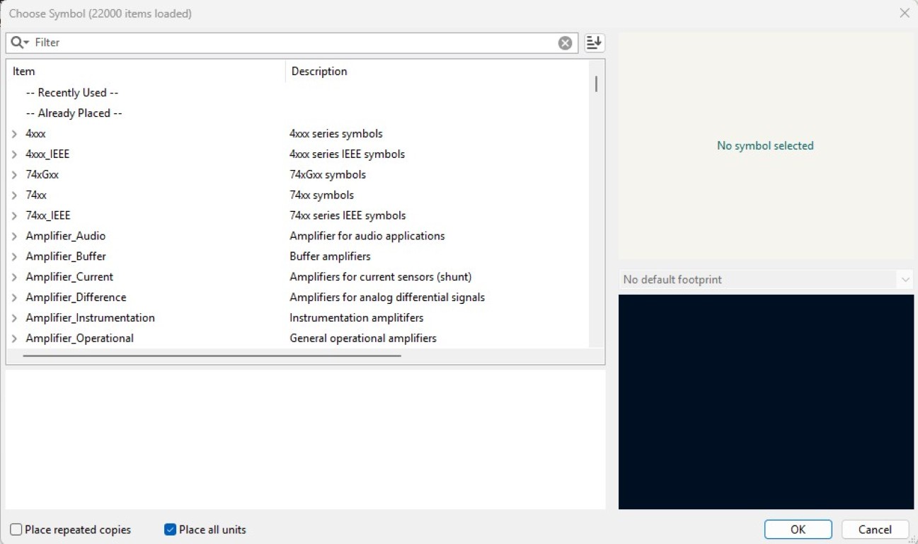
Now we start by loading our components into our schematic. We do this by selecting the "Place Symbol (A)" symbol in the right-hand bar. The following window should then open.
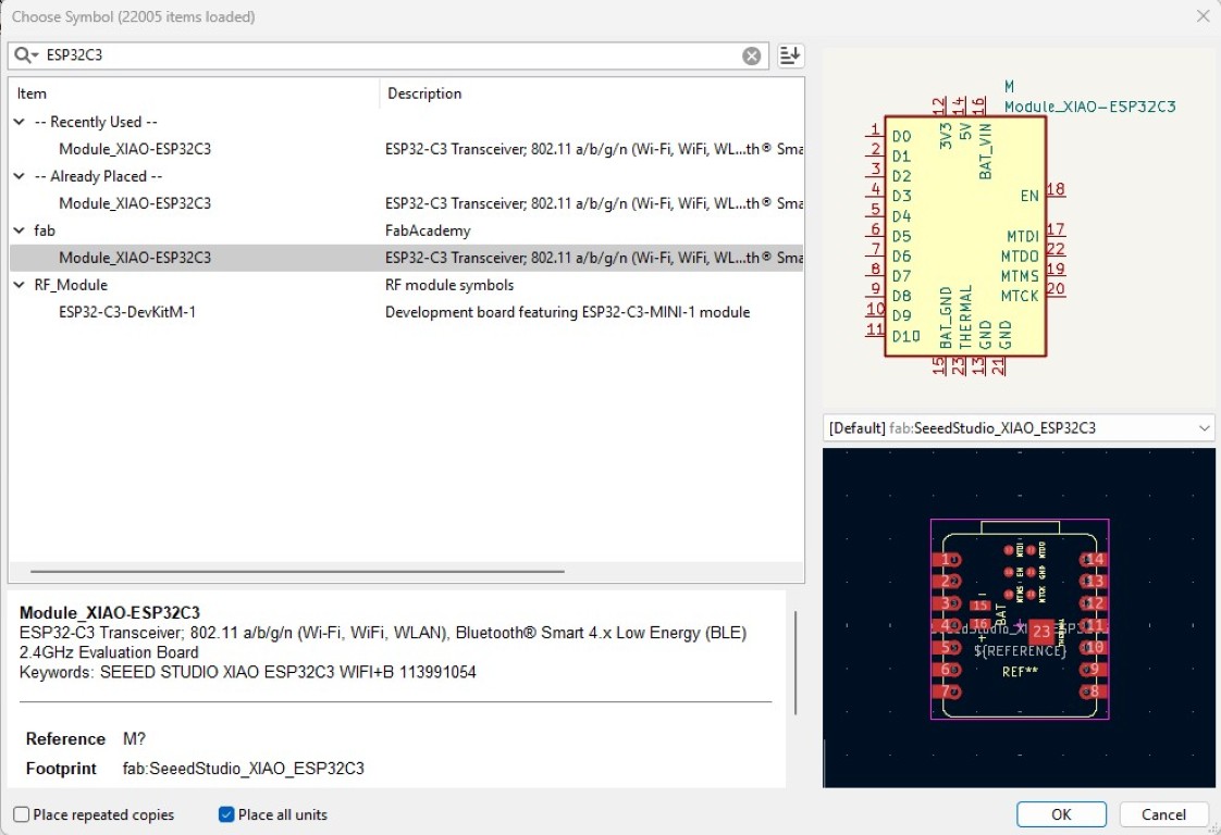
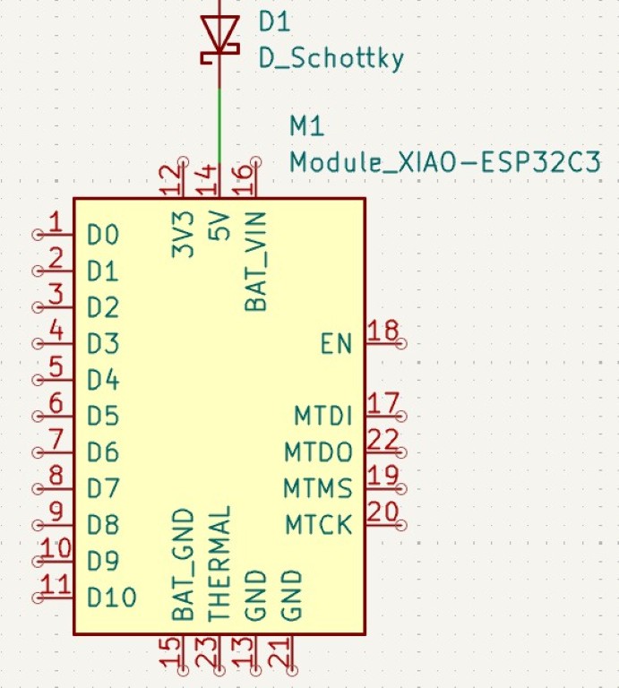
In the filter mask, I first look for our microcontroller, the ESP32C3. As shown in the picture, in the FabAcademy library we find exactly the ESP32C3 from Seed Studio that we
want to work with. On the right we see various previews of the component, below we find further specifications for the selected component.
Via the "OK" button we get our XIAO-ESP32C3 and can place it freely in our schematic with another click. Now it's all about continuing to build around the microcontroller. To do
this, I'm sticking closely to the data sheet and the manufacturer information,
which can be found here.
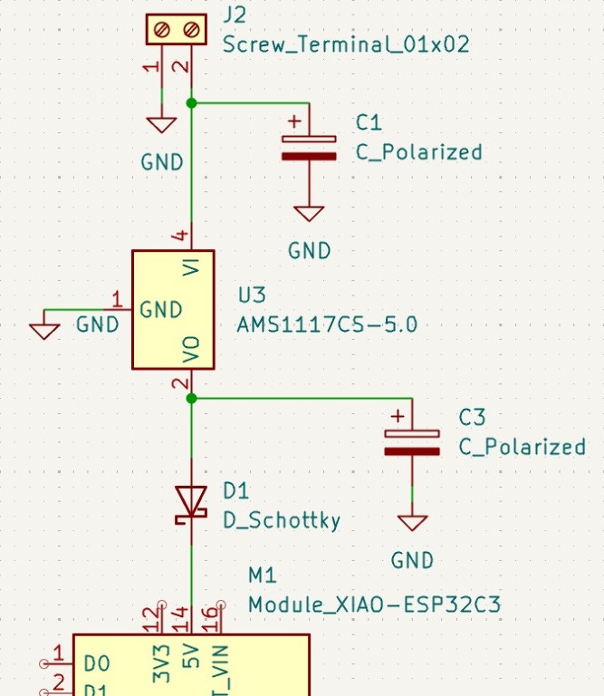
With a view to the final project and the intended mobile use, I would like to be able to operate my setups with batteries. Seed Studio provides the following information about the 5V port:
This is 5v out from the USB port. You can also use this as a voltage input but you must have some sort of diode (schottky, signal, power) between your external power source and this pin with anode to battery, cathode to 5V pin.
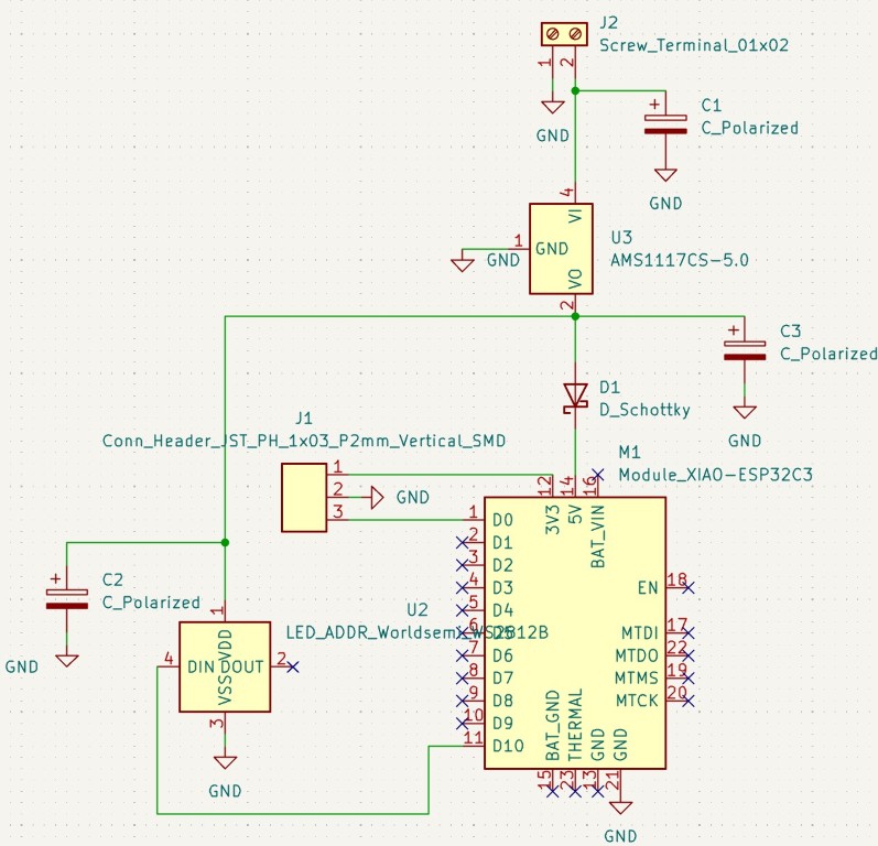
If we go into a little more detail, I inserted a 1206-sized schottky diode from the FabAcademy library using the same method as when inserting the microcontroller. This was initially displayed horizontally,
but if you select individual parts and press the "R" key on the keyboard, you can simply rotate all the components. I did this until the cathode was on the side of the 5V pin as required. Then I
connected pin 14 (5V) of the ESP32C3 to the cathode of the diode using the "Draw Wires (W)" symbol. These are the intermediate steps that led me to the following result.
Since I'm still undecided about which batteries I'm going to use, or whether I'm going to use existing batteries and combine them, I don't know what voltage I'll get as a result. It's very likely
that it will exceed 5V, so I'm using a step-down converter to ensure the 5V for the microcontroller.
From the data sheet of my chosen step-down converter, which is stored in the information in KiCad, I have information after installing it in my circuit about how to connect the respective pins of
the converter. To be honest, the data does not come from the first step-down converter that I wanted to use. I only used the AMS1117 on the recommendation of a colleague; before that I had a
step-down converter that would have required significantly more connections. So it was definitely worth changing; I just have to connect the voltage input and voltage output to ground with a bypass
capacitor and ground the ground itself. The input voltage comes from our battery and is connected or passed on via screw terminals. Accordingly, from the battery, + would be connected to screw terminal
two and - / GND to screw terminal one.
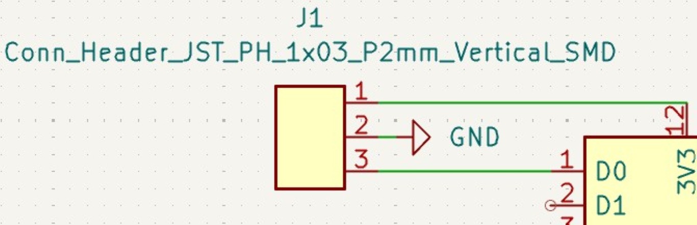
For the next part of my final project, I'll try to anticipate the vibration sensor. If possible, I'd like to work with piezoelectric sensors, but these generate high voltages and could damage the
microcontroller. Therefore, it requires many components and a complex circuit to be able to use them. In the interests of risk management, I'd like to initially outsource this to a single board
and continue during Input Device Week. Therefore, I'm only creating a JST header here to connect a sensor so that I can later establish a cable connection. For this, I need three pins, one for the
power supply, one for grounding and one for the analog signal. The recommendation in the data sheet states that, for analog signals, you should ideally use pins A0 to A2, or here designated D0 to
D2. I used D0 here.
Lastly for this week, I would like to test the installation of the WS2812b LED, which I want to use in the final project in the form of a string with an external power supply. For testing, however,
one LED is enough for me. According to the data sheet, the WS2812 requires a voltage between 3.5 and 5 V as an input voltage (VDD). Unfortunately, the ESP only supplies a voltage of 3.3 V and is
therefore not sufficient. The 5 V pin would be usable if I power the ESP via USB. In my situation, however, this is not the case, so I have to branch off the 5 V behind my step-down converter. The
data sheet also shows that a bypass capacitor is required here too. As before, this must be connected in parallel and pulled to GND, which is what can be seen in the picture. DIN stands for Data In
and refers to commands that are directed to the IC in the LED in order to control it. We do this via a digital pin on our ESP. VSS must be grounded. DOUT comes from the fact that the LEDs are typically
placed in series and pass on the control signals via an internal bus system, so that any number of LEDs can be controlled via just one data line. In our case, the internal IC does not need to pass on
any data, so this connection remains empty.
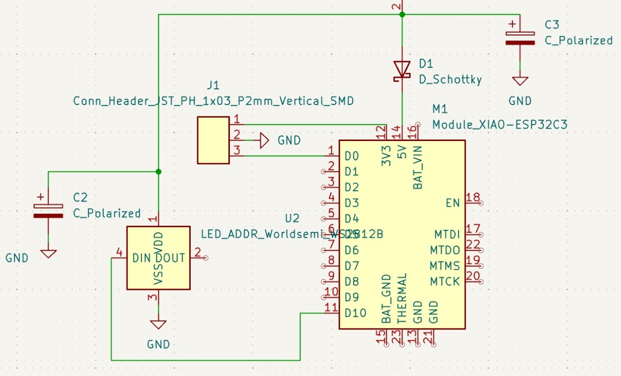
This completes the components that I want to install this week and that should enable communication and interaction with the microcontroller. Because nothing more needs to be added at this point, I
close all other pins by setting "No connection Flags (Q)" using the button on the right side. We can see the result in the picture.
So far, things have worked out pretty well - as is often the case in life, probably too well. So here is a small list of the errors and missing corrections that are still included in the circuit above:
the capacitor C2, parallel to the WS2812b LED, is not needed because the functionality is already provided by the capacitor C3, which is connected in the same way
the remaining capacitors C1 and C3 still have to be assigned values
the net labels have to be made known to the program
I have not set any power flags
I cannot use the GND pin that I used for grounding for operational purposes
I still have an incorrect step-down converter
How did I come up with this? Accompanied trial and error. Accompanied by both software and moral and technical support combined in the person of our instructor.
But first things first: I had my doubts about capacitor C2 because I thought it was duplicated. This was confirmed by our instructor. The next thing we need to do is assign the appropriate values to our
components. We get to the menu where we can do this by double-clicking on our component. For the example of capacitor C3, it looks like this. There we change the "value" entry.
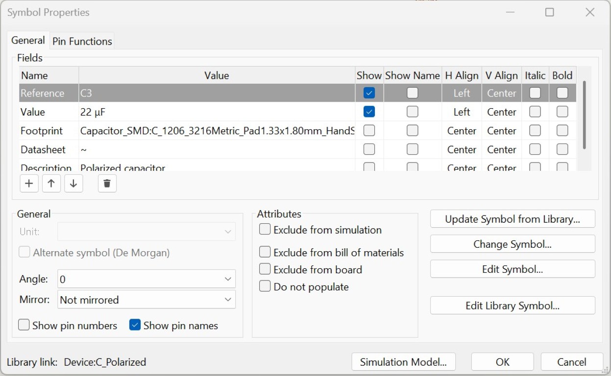
You may be wondering how I arrived at the value of 22 μF. You may also be thinking that I have asked myself this question too. I can confirm that. In my desperation not to find these values in the data sheet,
I initially sought help, which is how I switched to the AMS1117. To conceal whether the step-down converter I initially selected did not provide these values in the data sheet or whether I was just too stupid
to find them, I will not mention any names here. What I was very pleased about is precisely this information from the data sheet of the AMS1117. This information can usually be found in the data sheets, and is
probably also the case with the converter whose name cannot be mentioned.
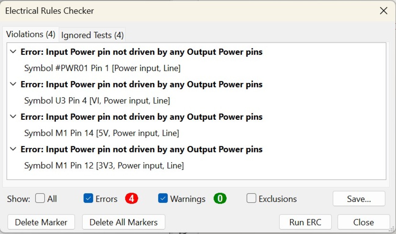
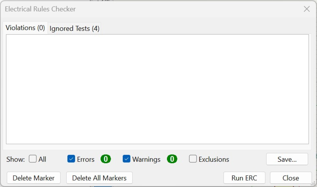
This brings us to the point where the net labels need to be made known. In the style of trial and error, I found this out myself using the electrical rules checker, which you can call up in the top bar relatively
far to the right and which you should call up whenever you think you are finished with the schematics. The check led me to the following result.
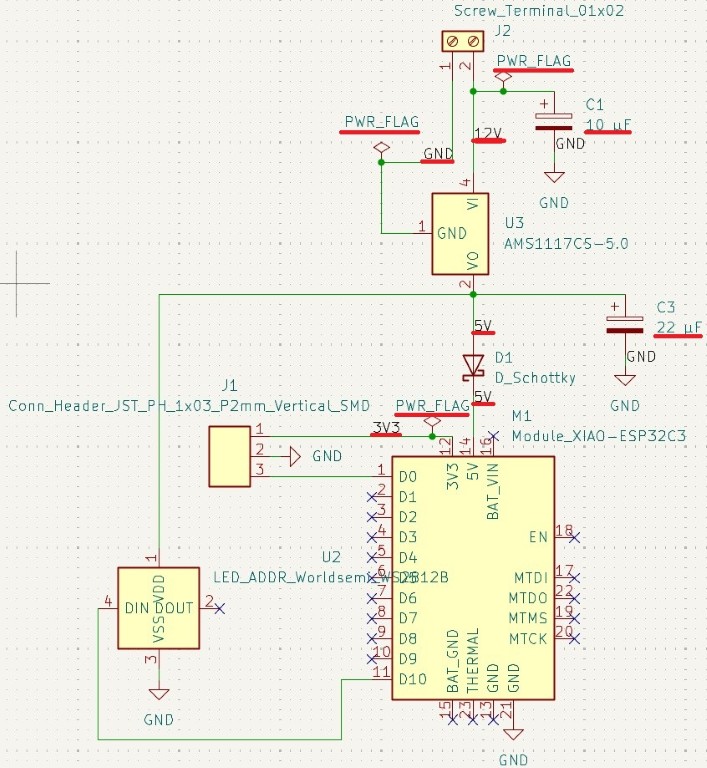
I was very happy to set about fixing these errors. First we need to tell KiCad where our power supply is coming from. We do this by using power flags. This is also done using "Place Symbols (A)" in the top right-hand
toolbar. Then we enter "PWR_FLAG" in the search field and set the corresponding symbol behind our voltage input on the screw terminal, both on the ground and on the supply voltage. I was only able to eliminate the
fourth error, the 3V3 on M1 pin 12, by inserting a power flag there too. The description of the power flag in KiCad is as follows: "Special symbol for telling ERC where power comes from" - don't forget to set it!
I also used the "Place Net Labels (L)" button to indicate which voltages are present on the lines. I created labels like this and then assigned them. Another source of error here is making the naming compliant with
German engineering guidelines. Here it is usual or required to use a space between the value and the unit; forget that if you use KiCad. 3.3 V should also not be written with a comma or period; it is referred to as 3V3.
With all these changes we arrive at the following schematic. Small spoiler here: It is not final. Changes are marked in red.
For now, we live with the reward of zero errors in the electrical rules check.
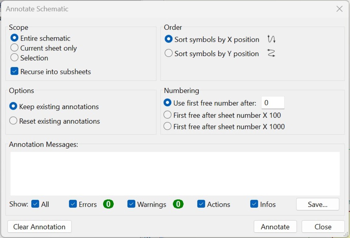
Next, we let the program execute the "Annotate Schematic" workflow. The button for this can be found relatively far to the right in the top bar. Clicking on this will bring up the following menu, which we only have to
confirm at the bottom by clicking "annotate".
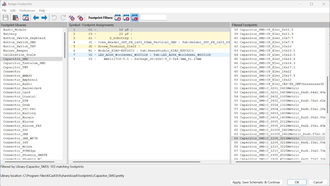
What we can also do in the schematic is to assign the footprints. The button for this is slightly to the right of the one we used to annotate the schematic. The following menu opens here.
It is not easy to find the right footprints here. If you are unsure about this, I would recommend that you seek advice. I also asked my instructor for advice. In general, the menu displayed does not contain footprints
for the yellow-highlighted components. Footprints are cutouts that we have to make to mount the component on the circuit board. In general, we can find broad categories in the footprint libraries on the left, and after
clicking on them we get plenty of specific options in the right-hand column. The selection can be difficult here. With support, I was able to manage it myself.
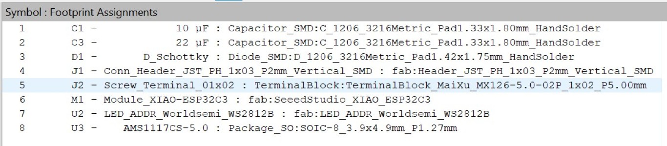
My footprints are or were the following.
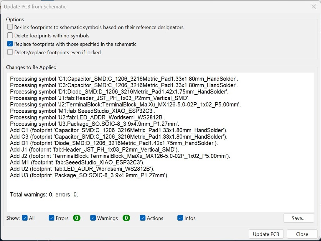
Once we have mastered this step, we can select Tools > Update PCB from Schematic and in this way get closer to our PCB. In doing so, we run another test that fortunately cannot find any errors. We can then continue by
clicking on "Update PCB" at the bottom right.
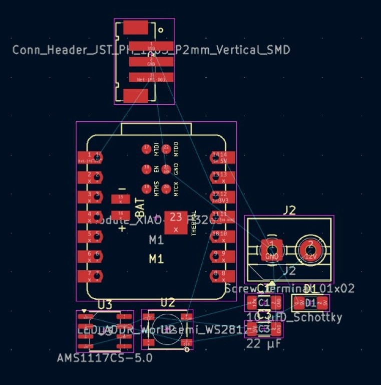
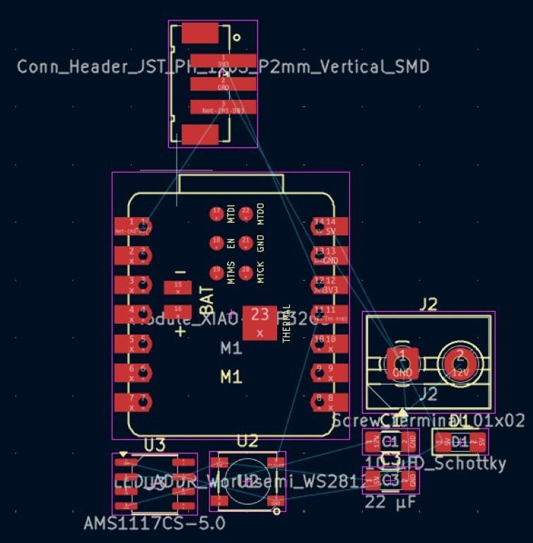
This brings us to the following PCB. We still have to arrange it ourselves. Here, too, we can grab and move the parts and rotate them using the "R" key on our keyboard.
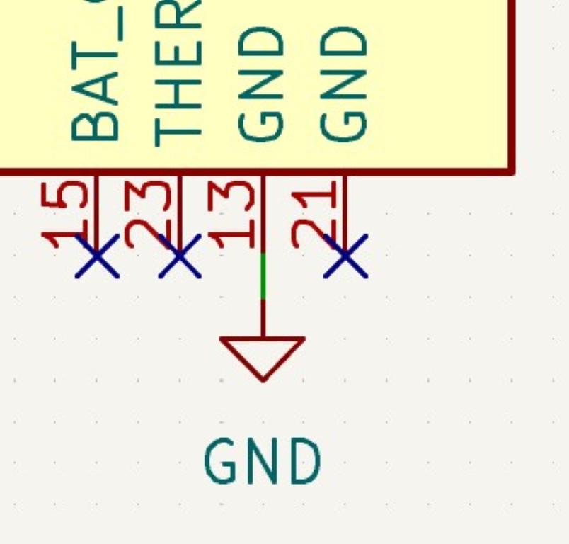
Let's go back again: How do we know that we are using the wrong ground pin?
Our beautiful board from XIAO with the ESP32C3 has two sides. On the underside there is a GND pin, pin 21. In order to use this, however, we would have to solder on the underside of our board. I imagine that would be
complicated, even if it would be possible in principle. This leads me to jump into the schematic and put the connection to ground pin 21 on pin 13 and at the same time set a no connection flag on pin 21. Could this
have been known? Maybe. Will this mistake happen to me again in the future? For sure.
With this short and fun excursion, now back to the PCB Editor. The connections to ground, thinly indicated in light blue, now look much more feasible. But somehow the AMS1117 suddenly got more pins. How did that happen?
I selected the wrong one when inserting it and inserted the AMS1117CS-5.0 rather than the AMS1117-5.0. I find it a little incomprehensible that the difference was not already shown in the schematics, but that can also be
reversed. So I jumped into the schematics here too and swapped the step-down converter. From this bulge of possible versions that I could choose from. You really have to be careful here or have a lot of fun reversing your
circuit afterwards.
After making such changes, it is important to switch back to the PCB Editor from the schematics via Tools > Update PCB from Schematic. If you change the components, you should also check the box "Delete footprints with no
symbols" in the options. Only then will the old step-down converter be deleted from the PCB. Any questions about how I found this out?
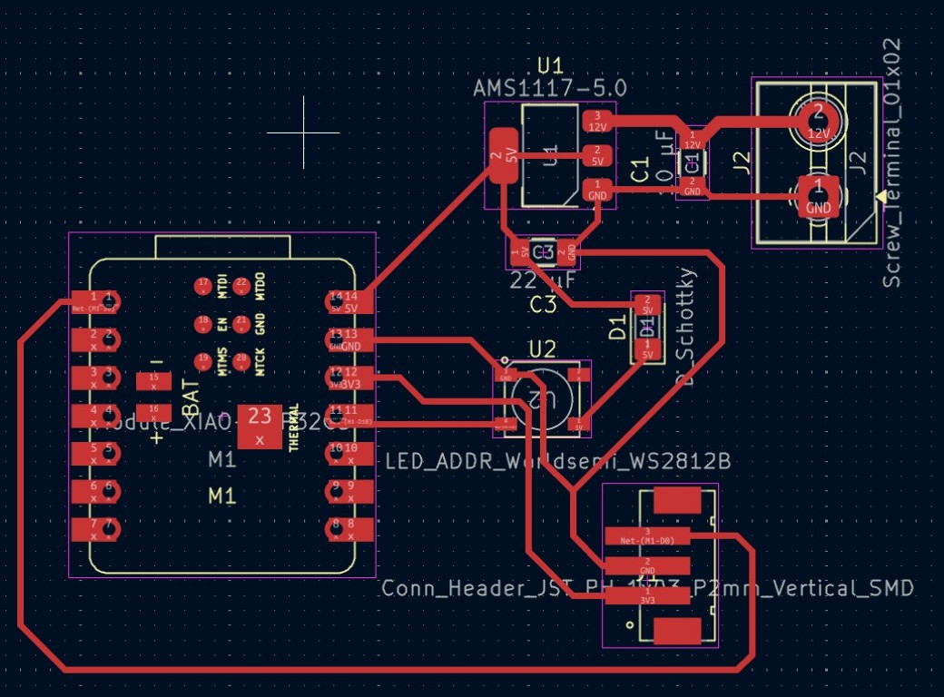
Now comes the coolest part of the PCB design for all Tetris fans. We have to distribute and rotate the components on the board so that we can draw lines without crossing conductor tracks. First the arrangement, then we
can draw the individual connections in the right-hand bar using the "Route Single Track (X)" button. At this point I hope you have fun and I'll cut it short for myself, here is the result of my wiring. We can also go
under components with a clear conscience, but we shouldn't make it too tight so that we can solder everything well later and it fits correctly.
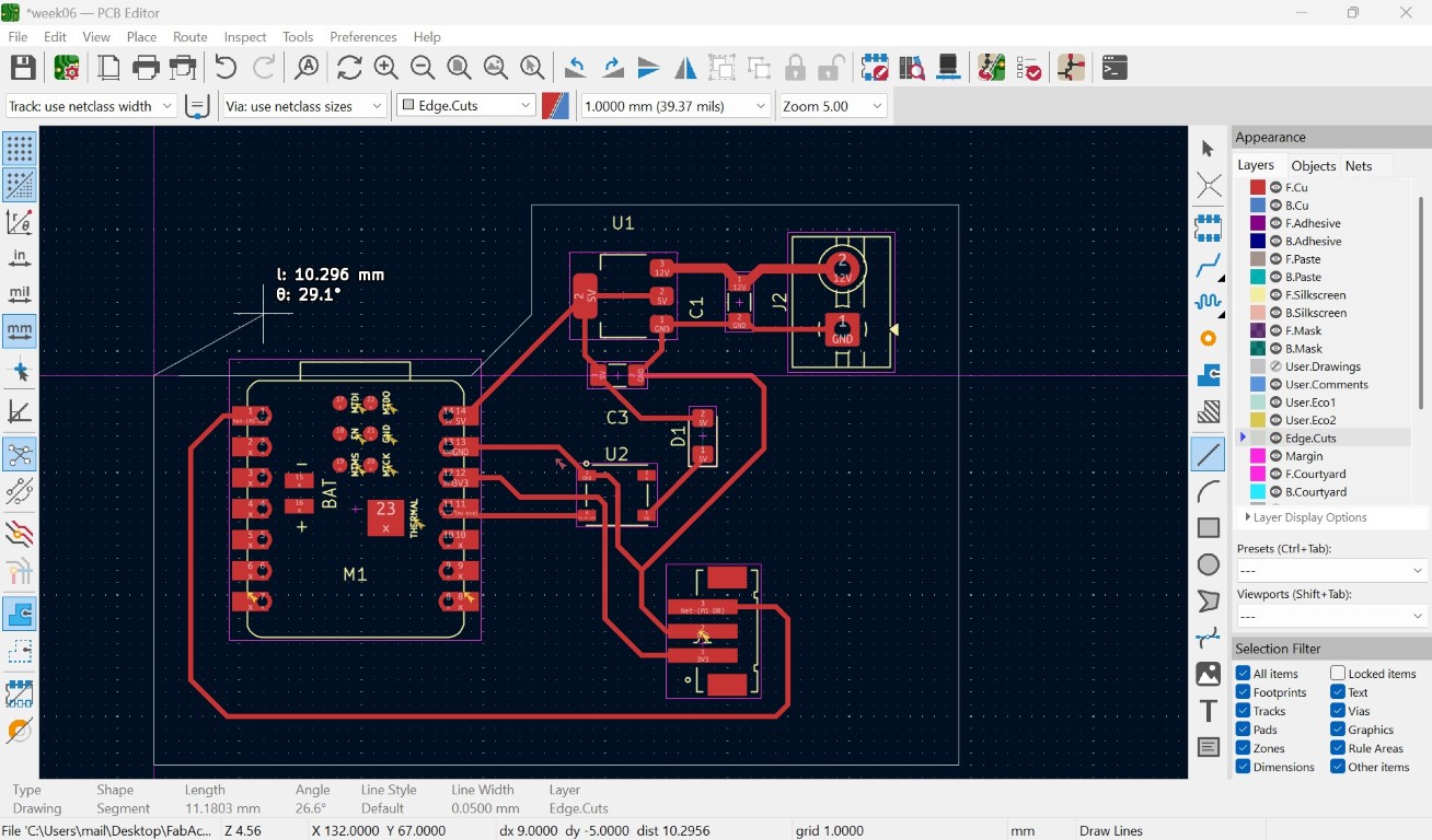
Finally, we need to draw an outline for our circuit board. We do this by first selecting the edge cut layer in the right-hand selection area for the different layers and colors. Then we can use the drawing tools on the
left to draw straight lines, circular arcs and anything else our heart desires. It is important to connect the start and end points cleanly, as I do in the last step as shown in the picture.
Last but not least, we run the "Design Rules Checker" on our PCB. It complained to me because the labels of the individual components, which can still be seen in the second to last picture, are cut by cables and components.
In addition, the silkscreen is clipped by solder mask and board edge, but this can probably be ignored.
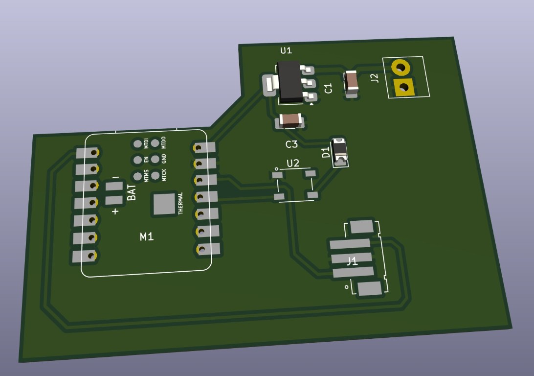
That's it for this week, there are still some problems with the Gerber file in KiCad 9.0. As soon as these are resolved, I will attach a Gerber file below. Until then, the KiCad file will have to suffice. The final part is
the 3D model of my PCB, although it is unfortunately not complete due to missing models of individual components.
Download this weeks files
KiCad-Project