
Week 8: Electronics Design
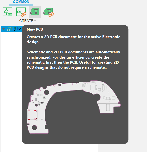
In my pursuit of the best PCB design software, I initially intended to use Eagle from Autodesk. However, Autodesk has recently announced that Eagle will become obsolete by 2026. Consequently, its functionality has been seamlessly integrated into Fusion 360, which combines PCB design with 3D modeling capabilities. Therefore, I decided to utilize Fusion 360 for all my PCB designs.
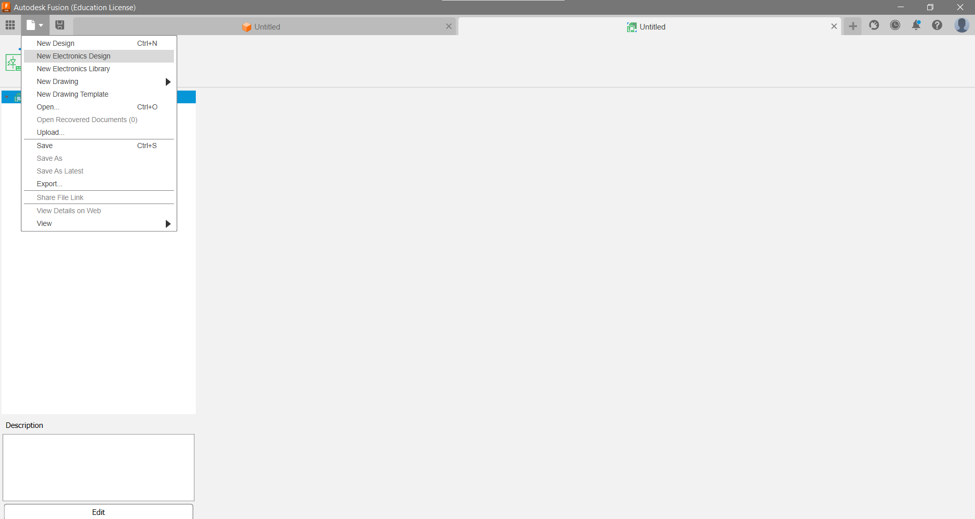
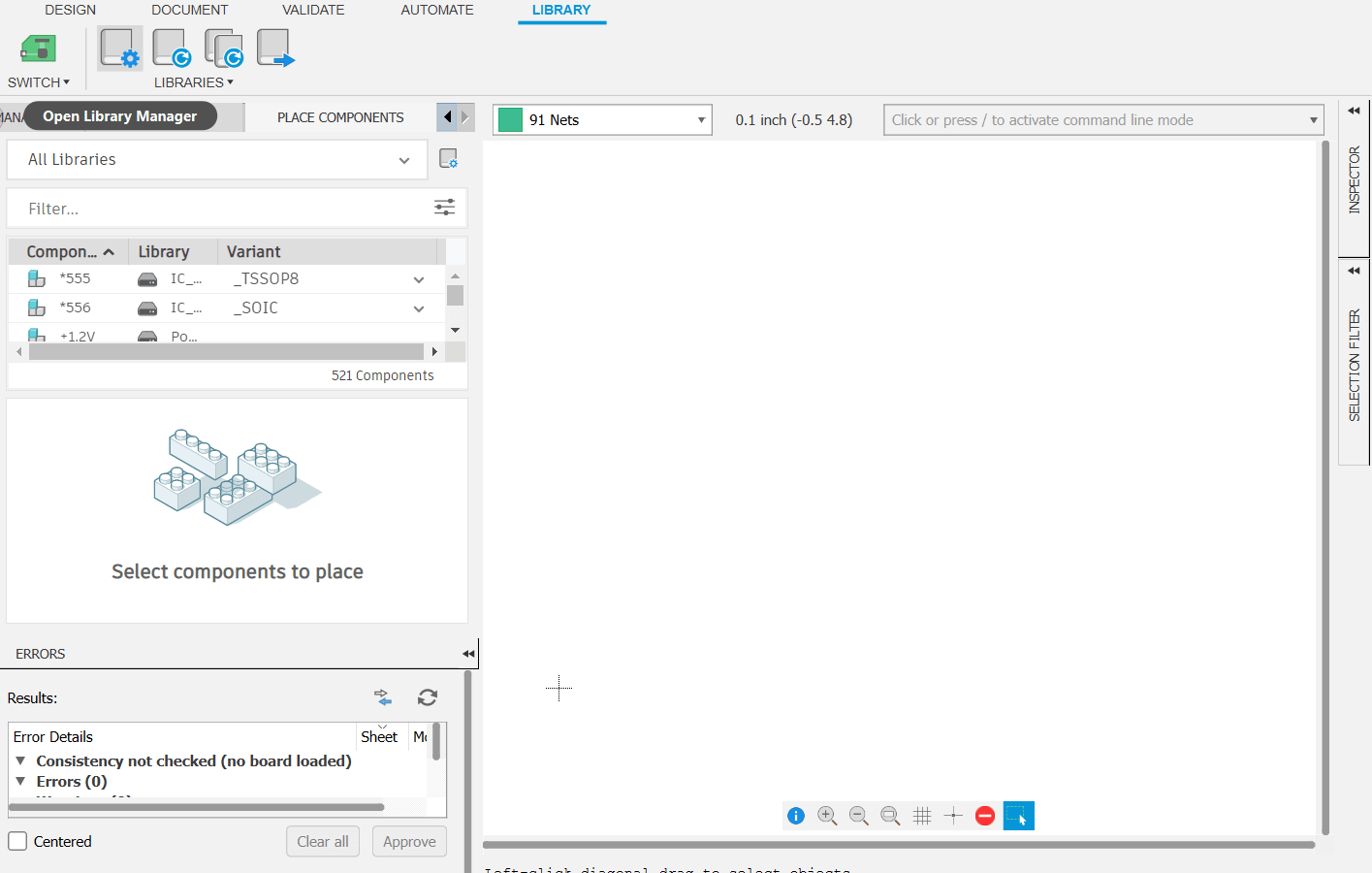
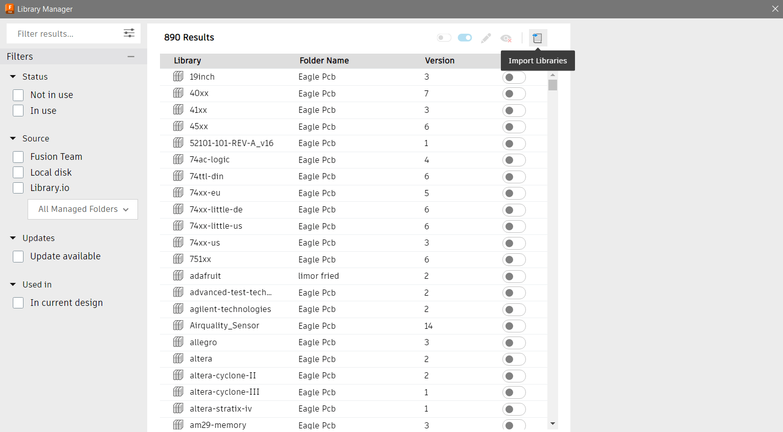
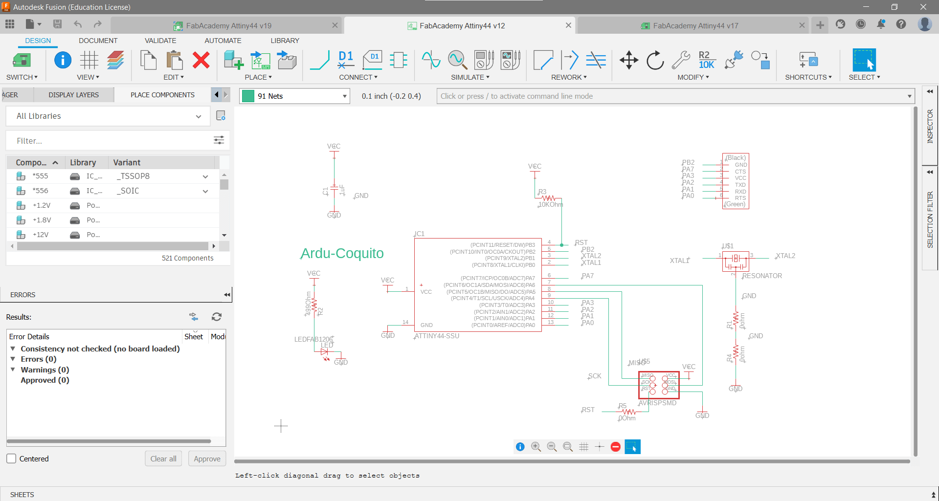
The first step is to open Autodesk Fusion, then create a new electronics project. After creating the project, the next step is to design the schematic of the electronic board. To do this, libraries with the components to be used must be added. In my case, I used the Fab Academy library. However, since Fusion integrates both the footprint and the 3D model of the components, the Fab Academy library does not include detailed 3D models of the available components.After adding the library, the next step is to design the schematic by making the corresponding connections according to the datasheet of the microcontroller and the rest of the components to be used.
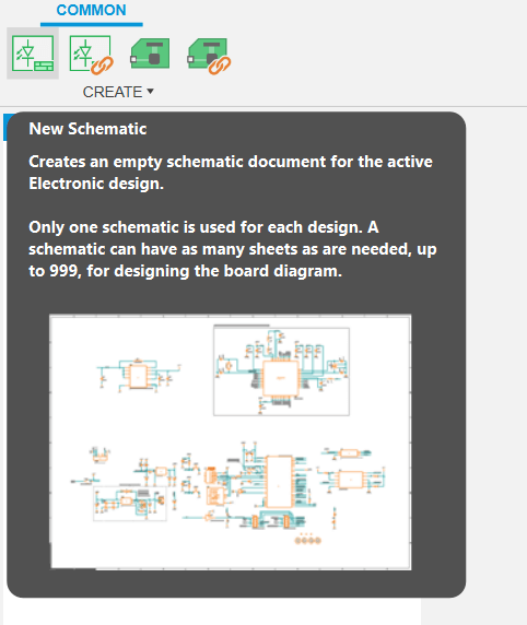
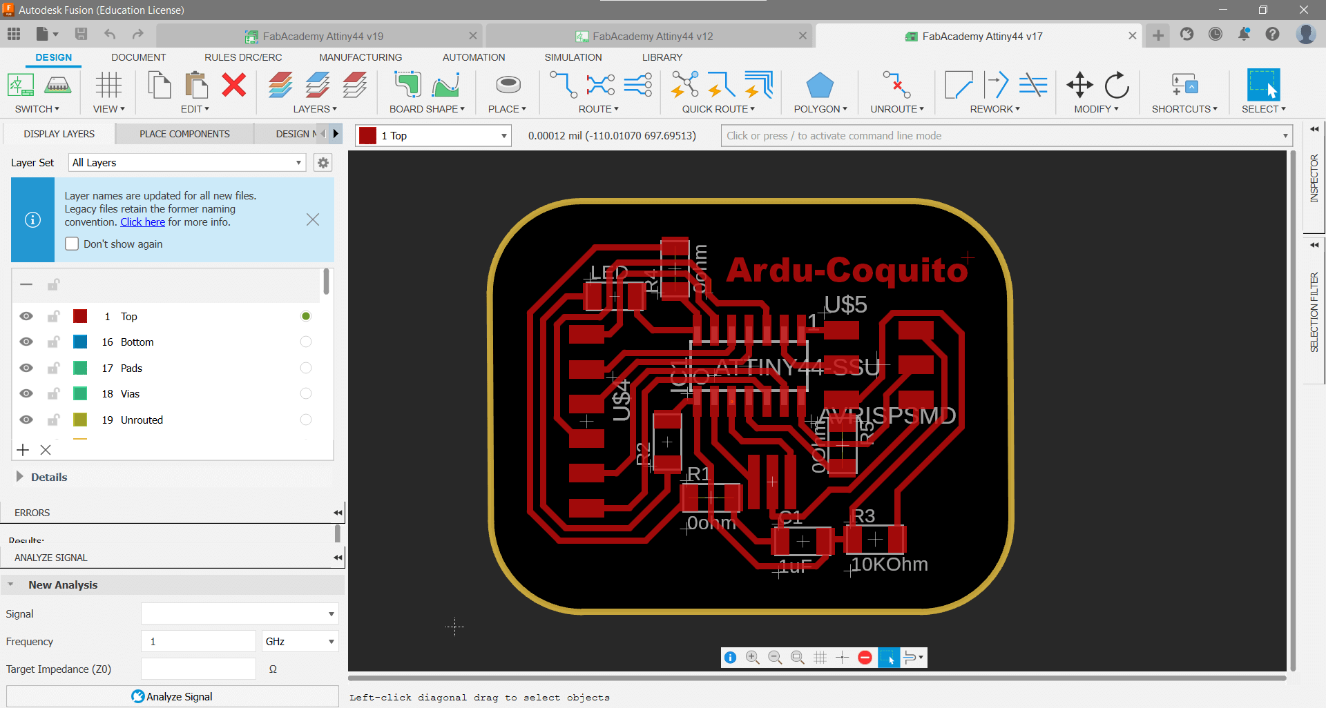
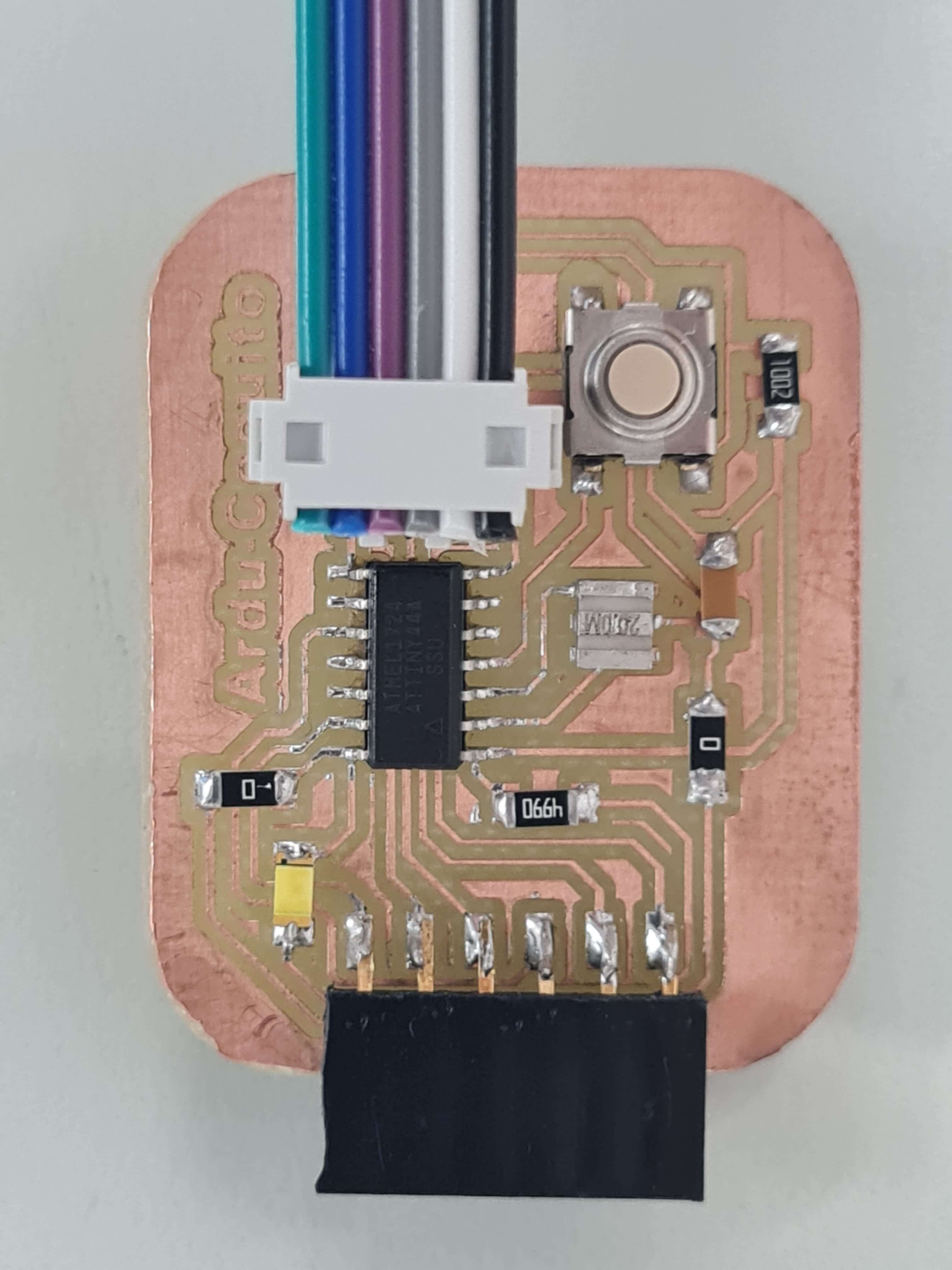
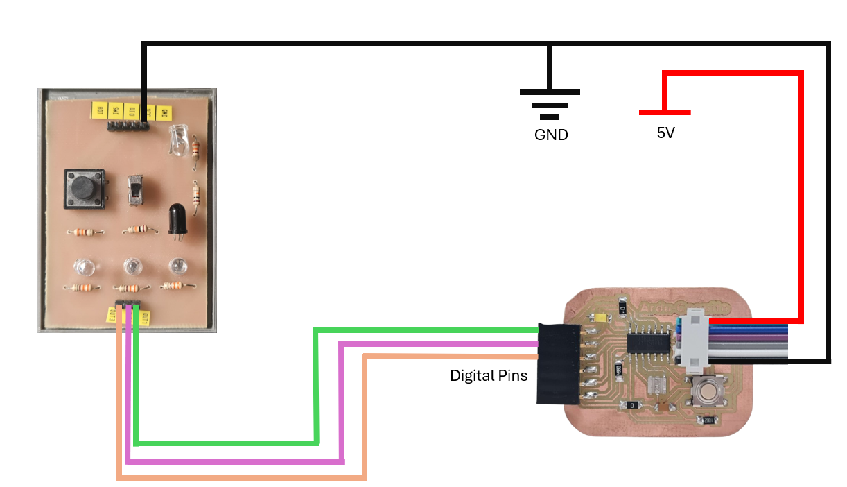
After adding the library, the next step is to design the schematic by making the corresponding connections according to the datasheet of the microcontroller and the rest of the components to be used.In my case, I had to place a 1uF capacitor between VCC and GND to filter the input voltage. Additionally, a 10kohm resistor was added to the reset pin of the Attiny44 microcontroller and a external 20Mhz cyrstal oscillator.
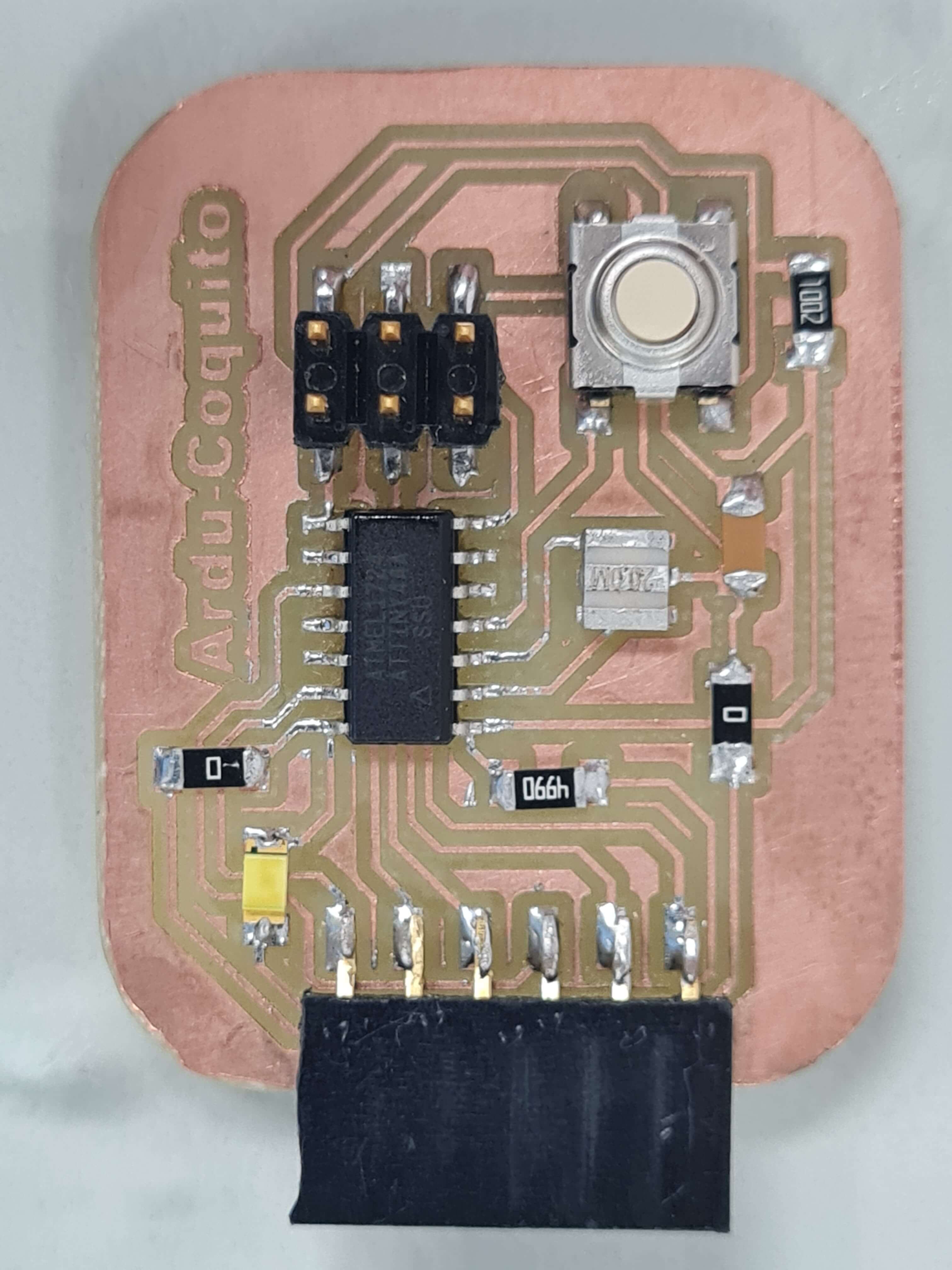
To design the PCB layout effectively, it's crucial to prevent crossovers between traces. This requires a careful distribution of components and traces. In cases where crossing traces is unavoidable, a 0-ohm resistor is used. This component allows up to two traces to pass beneath it, effectively acting as bridges. The criterion I used for distributing the electronic components was to identify where the highest number of connections were located and place this component as close as possible to them. This ensures that I can connect the majority of pins directly, and in the worst-case scenario, cross the remaining traces.
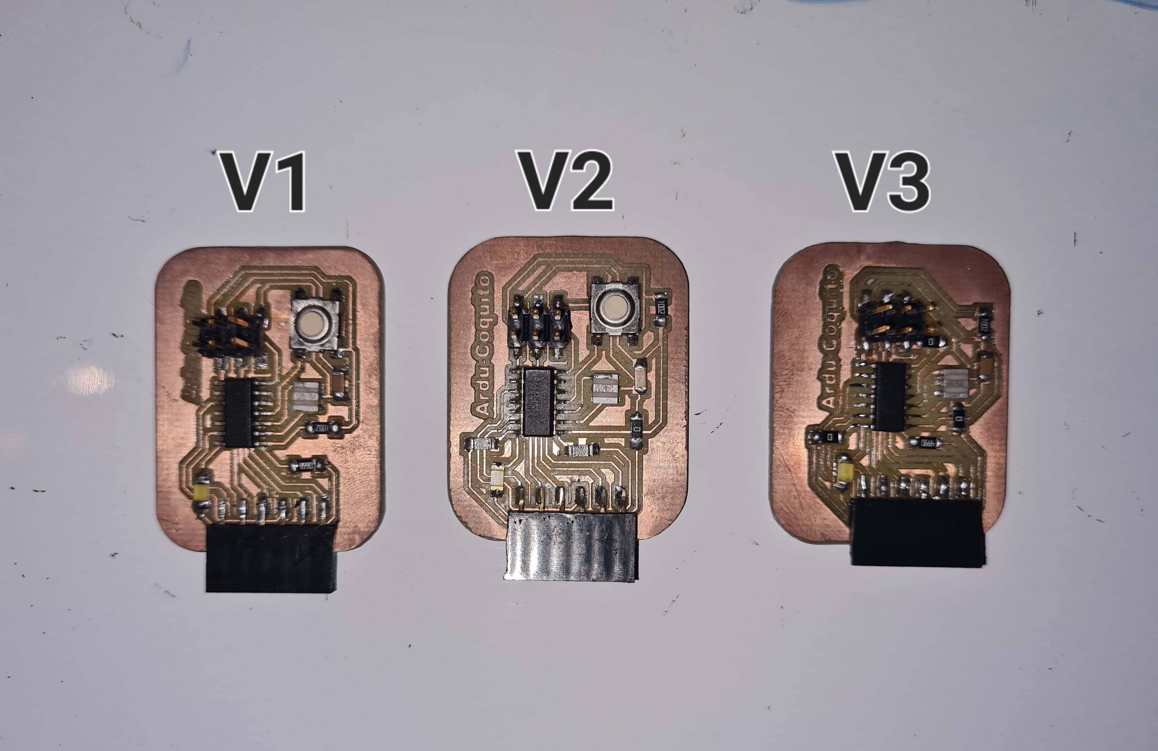
Another trick is to use existing components as bridges. The idea is to position them in such a way that they also serve as bridges. For example, resistors, capacitors, buttons, or even the microcontroller itself can be used to avoid crossing traces and minimize the use of 0-ohm resistors.During the design process, I underwent three iterations because the board failed to compile and upload the microcontroller. The issue stemmed from missing ground connections, which were not properly labeled in my schematic.
In this design, I used 16mil traces, which turned out to be too narrow and delicate. For my future designs, I plan to use 30mil traces. While the wider traces mean I can only pass one trace above a resistor or LED instead of two, the benefits outweigh this limitation. Using 30mil traces will result in a more robust board that is easier to solder and manipulate. This change will improve the durability and reliability of the board.
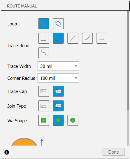
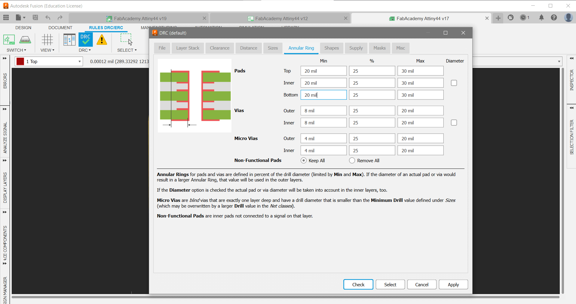
Sometimes, default pad sizes are too small, which can lead to issues with board durability and reliability. To address this, I plan to use the DRC (Design Rule Check) tool in my next designs to increase the pad size. It's important to note that if I increase the pad size too much, they can potentially collide or interfere with each other. Therefore, I will ensure that the distance between pads allows for at least two passes of isolation by the V-tip mill. After making these adjustments, I will export the design to GRBL and use FlatCAM to verify that all distances are correct. This approach will significantly enhance the robustness and reliability of the board.
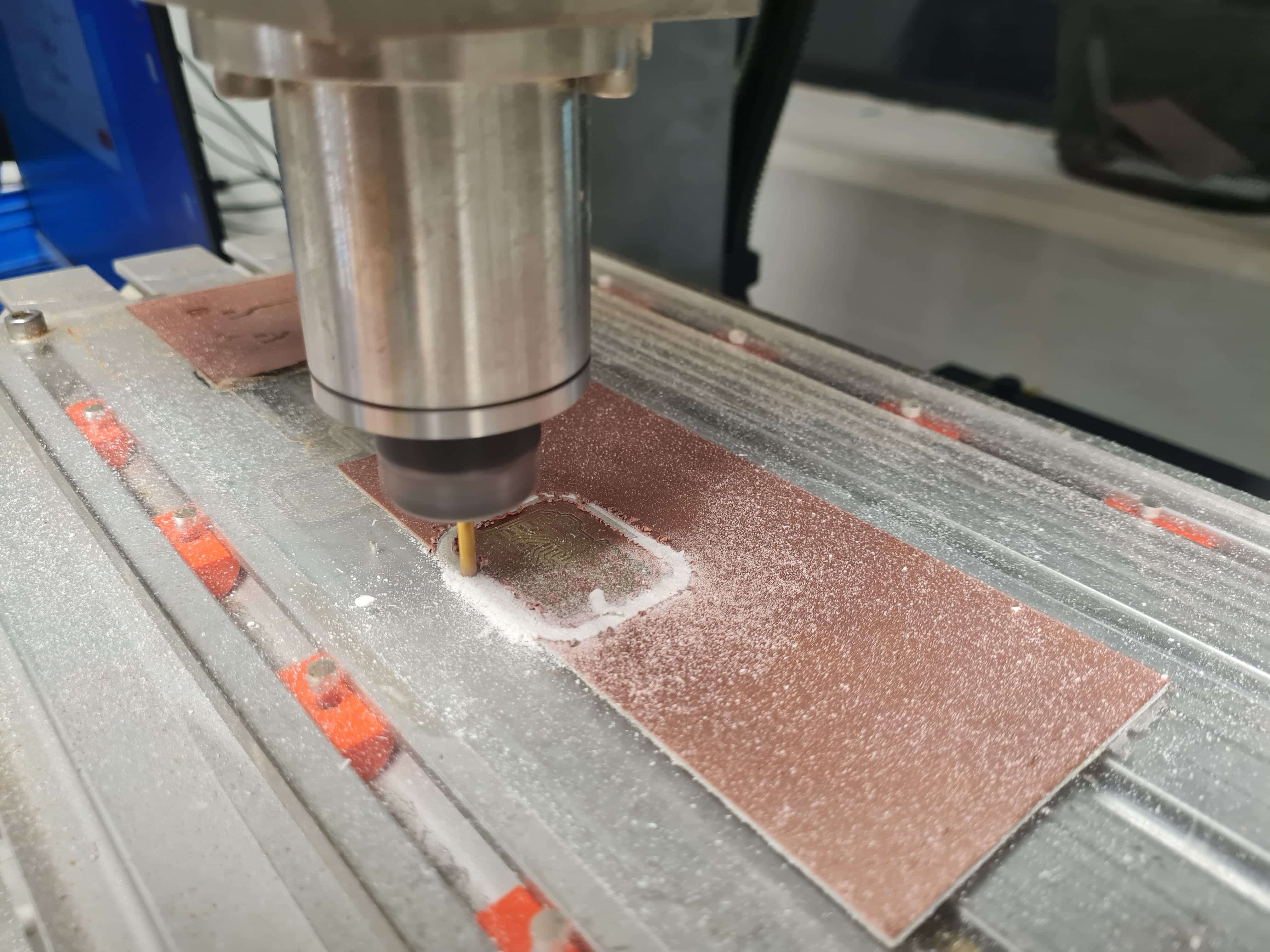
I personally designed all the PCB myself. I chose not to use the autoroute tool and instead preferred to manually design each board for the FAB ACADEMY from scratch.
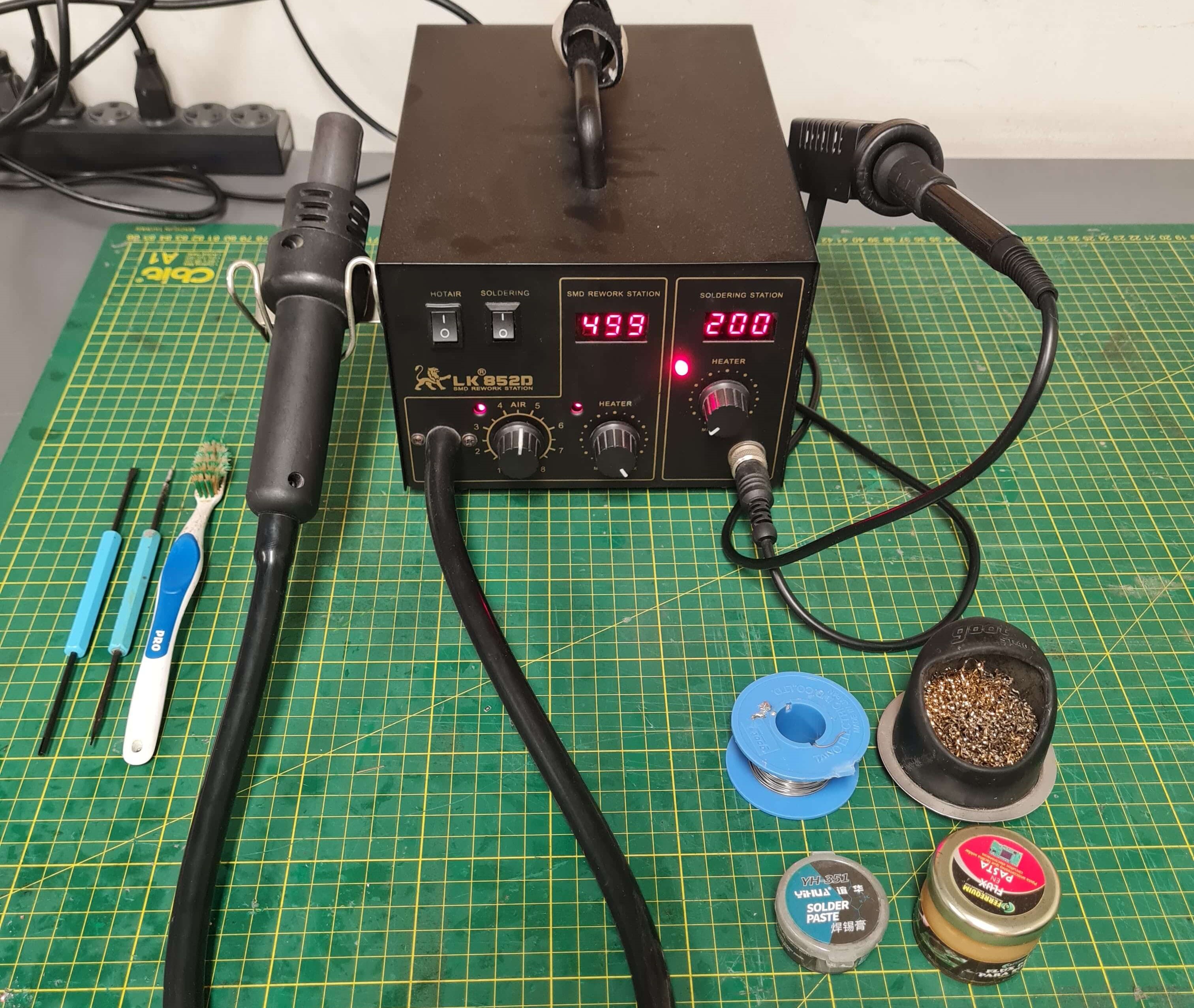
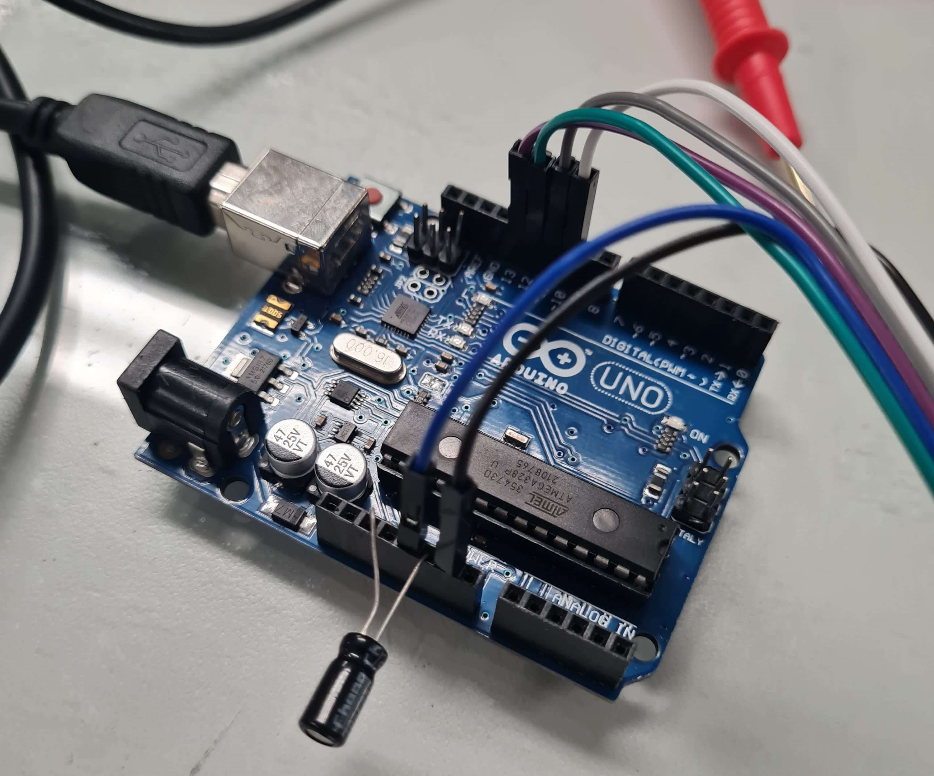
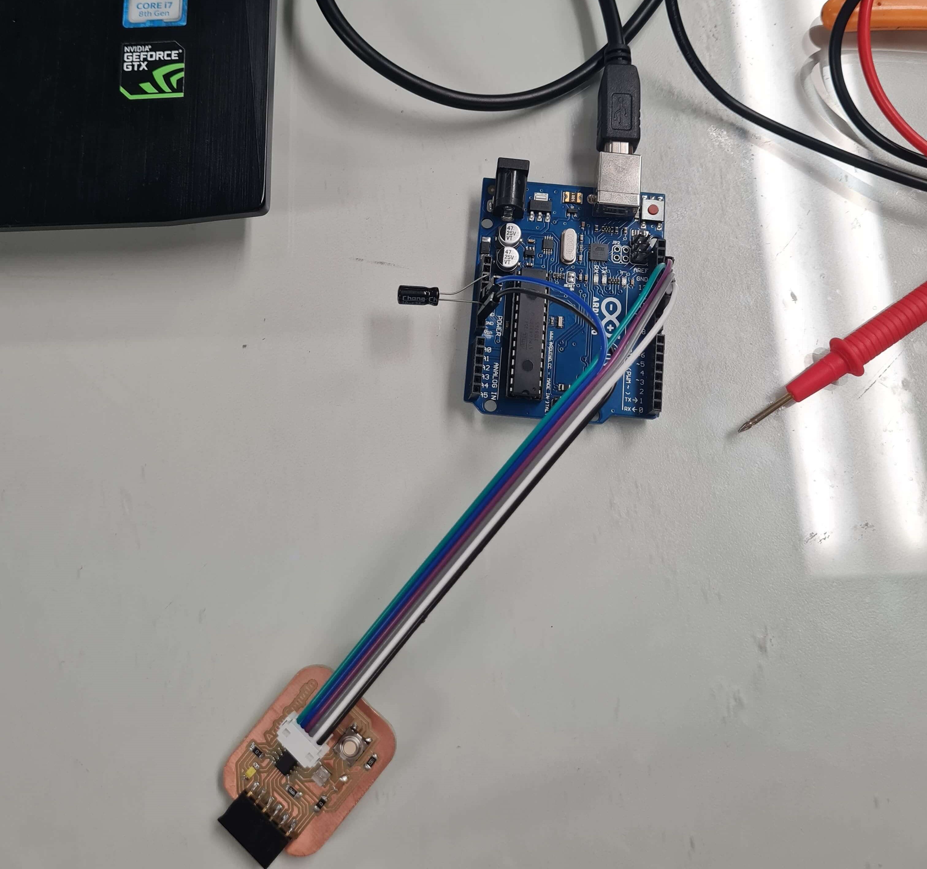
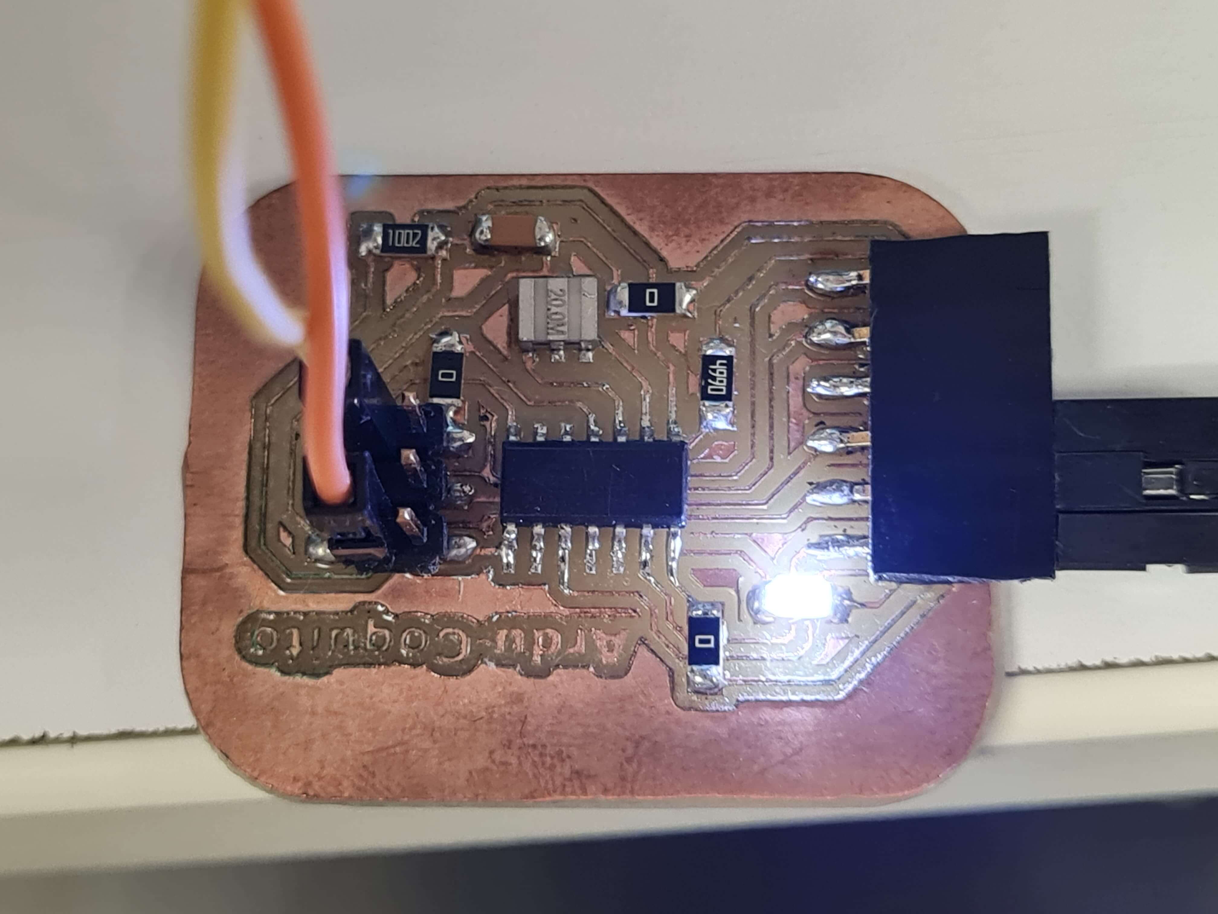
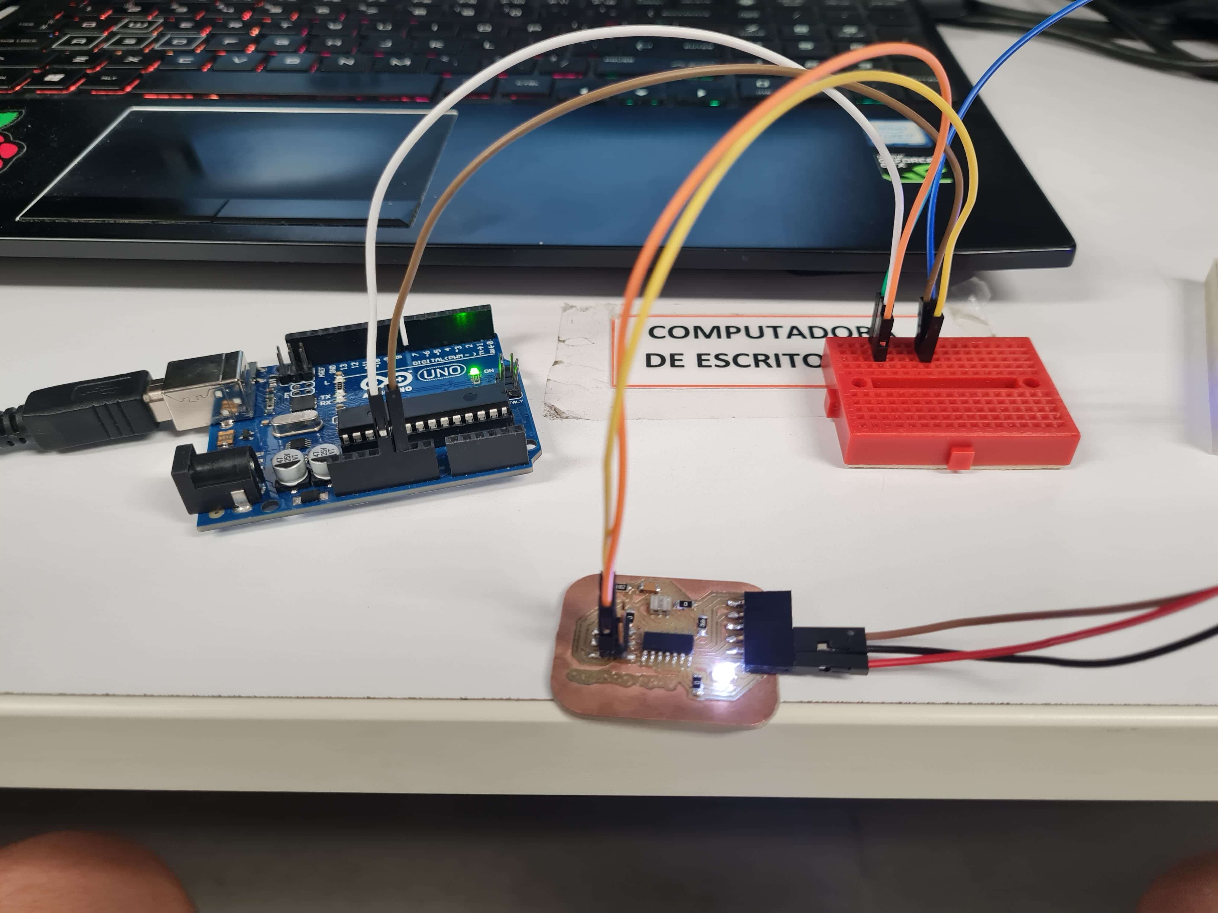
This week's assignment involved using lab equipment to observe the operation of a microcontroller circuit board.
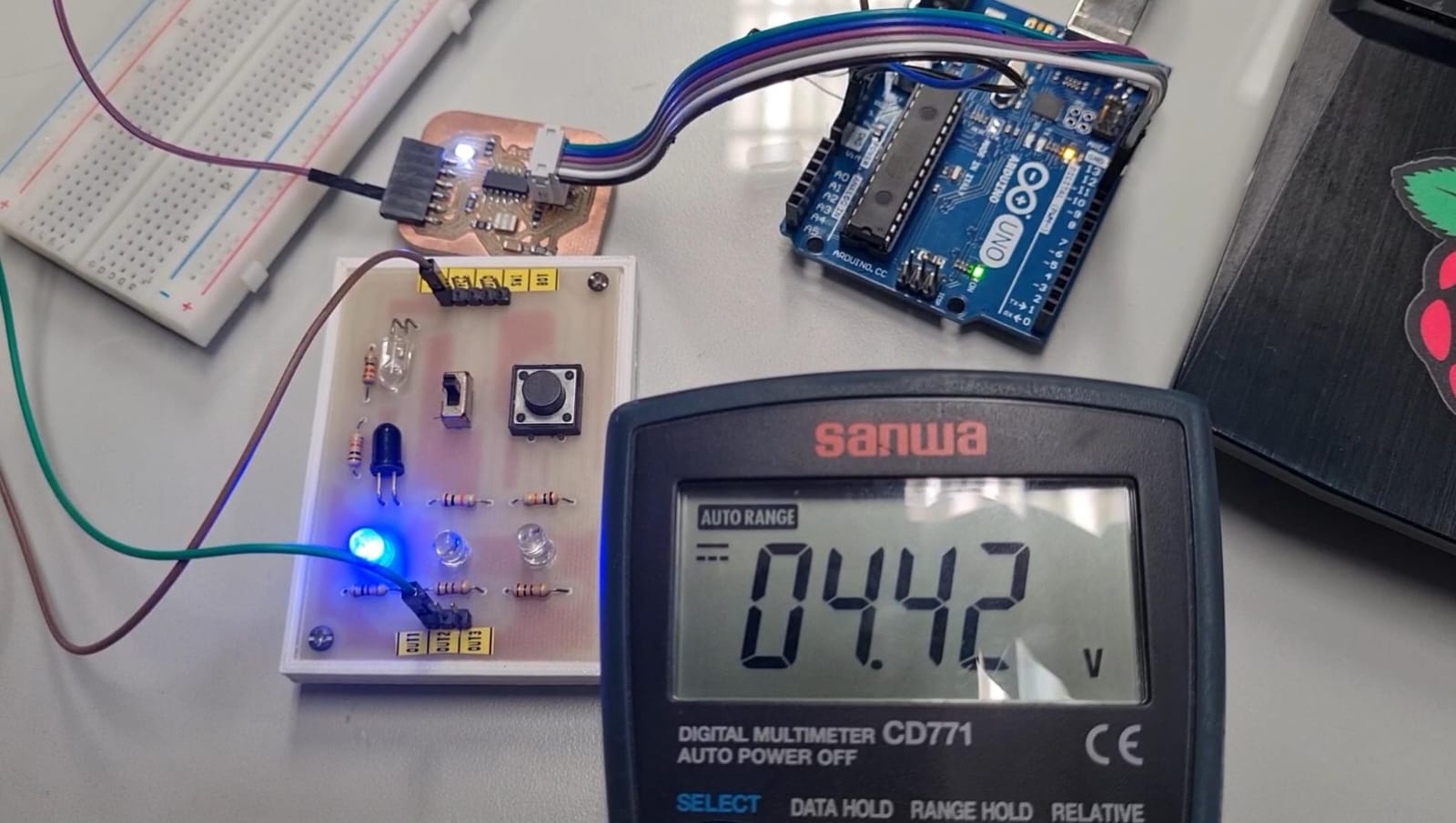
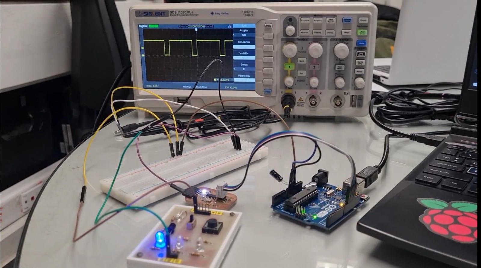
By doing this, we could see how the signals generated by the ATtiny44 changed over time, and how these changes affected the LED's behavior.