
Week 8
Electronics Design
Electronic Design refers to the process of manufacturing electronic components or devices, typically involving the assembly of various electronic parts into finished products. This includes activities such as designing circuits, creating prototypes, sourcing components, assembling PCBs (Printed Circuit Boards), programming microcontrollers, testing functionality, and packaging final products for distribution. Electronic production encompasses a wide range of industries and applications, from consumer electronics like smartphones and laptops to industrial equipment, medical devices, automotive systems, and more.
Our task for this week is:
Group assignment:
- Use the test equipment in your lab to observe the operation of a microcontroller circuit board (as a minimum, you should demonstrate the use of a multimeter and oscilloscope)
- Document your work on the group work page and reflect what you learned on your individual page
Individual assignment:
- Use an EDA tool to design a development board to interact and communicate with an embedded microcontroller
Group Assignment
The group assigment link is available here on the fabalab page.
This week, we delved into the intricacies of PCB design using Kicad software, mastering the art of crafting intricate circuit boards. As a result of our efforts, we were able to seamlessly transition from design to reality by printing out the PCB. It's been an enlightening journey, empowering us with practical skills in electronics and engineering.
What KiCad? A KiCad software is an KiCad is an open-source software suite primarily used for electronic design automation (EDA), specifically in designing printed circuit boards (PCBs). It offers a comprehensive set of tools for schematic capture, PCB layout, and component footprint creation. Here are some key features and capabilities of KiCad software:
1. Schematic Capture: KiCad allows users to create electronic schematics using a user-friendly interface. Components can be added from libraries, and connections between them are easily defined.
2. PCB Layout: The software provides tools for designing the physical layout of PCBs. Users can place components, route traces, define copper layers, and manage board dimensions.
3. Footprint Editor: KiCad includes a footprint editor that enables users to create custom footprints for components not available in the standard libraries. This is crucial for accurately representing the physical dimensions and pin configurations of components on the PCB.
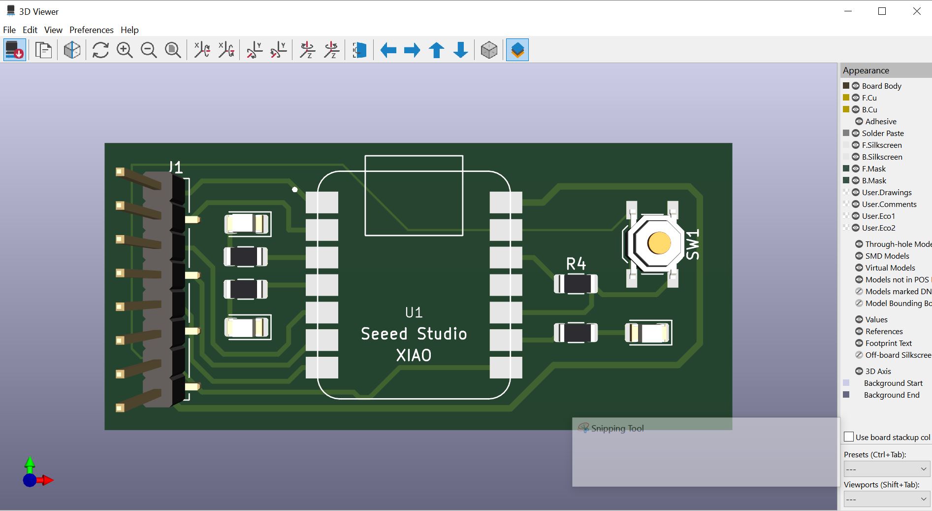
4. 3D Viewer: KiCad has a built-in 3D viewer that allows users to visualize their PCB designs in three dimensions. This helps in checking for clearances, component heights, and overall aesthetics.
5. Design Rule Checking (DRC): The software includes DRC tools to ensure that designs adhere to specified design rules, such as minimum trace width, clearance between traces, and minimum drill size. This helps in detecting potential errors or issues before fabrication.
6. Gerber File Generation: KiCad can generate Gerber files, which are industry-standard files used by PCB manufacturers to fabricate PCBs. These files contain information about copper layers, solder mask, silk screen, drill holes, and other necessary details.
7. Integration with Other Tools: KiCad supports integration with external tools and formats, allowing users to import/export designs in various file formats like STEP, DXF, and IDF. This facilitates collaboration and compatibility with other EDA tools.
Overall, KiCad is a powerful and versatile tool for electronics engineers, hobbyists, and professionals alike, offering a robust set of features to support the design and development of PCBs.
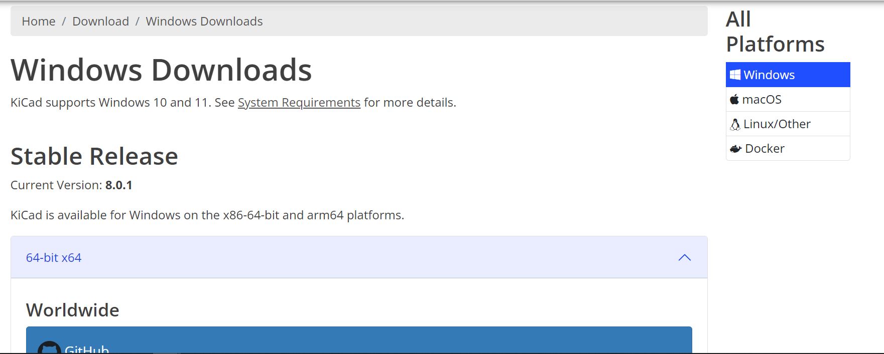
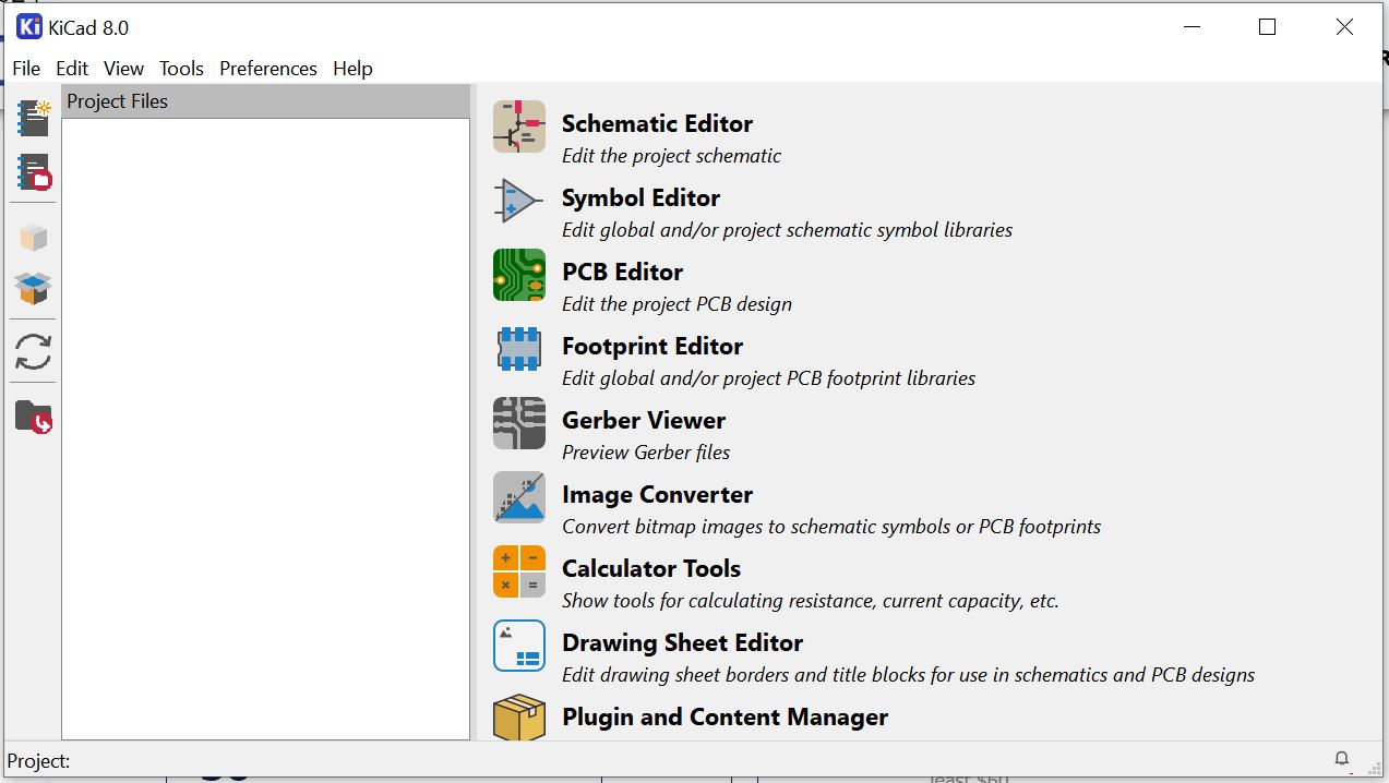
First, I began by obtaining the software and installing the setup on my computer.
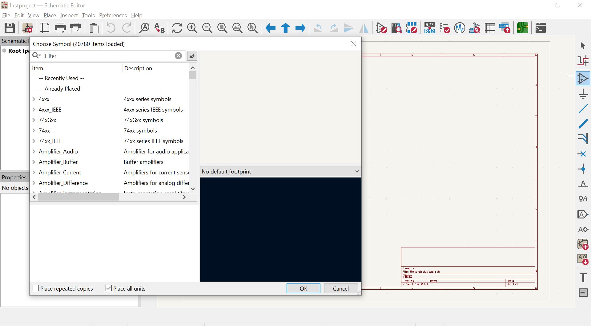
We began our customized PCB design process by configuring the settings to determine where to save our files and selecting the appropriate symbols required for our project from KiCad.

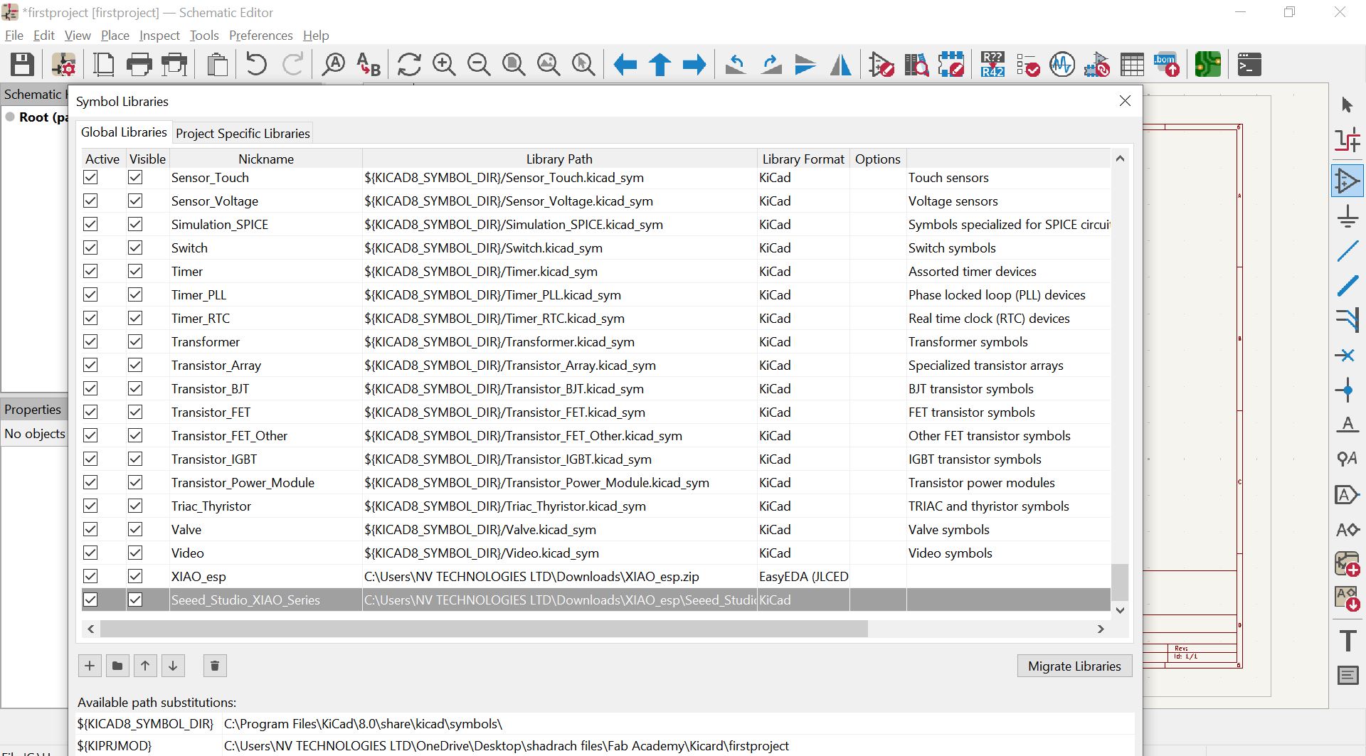
We imported the Xiao board into KiCad software
I connect components using wire symbols and apply skills to edit these symbols by deleting any unwanted elements within them. This editing process allows me to precise customization and arrangement of components on the schematic diagram, ensuring accuracy and clarity in the design. By efficiently managing symbols and their connections, designers can create organized and functional schematics that serve as the foundation for PCB layout and electronic production.

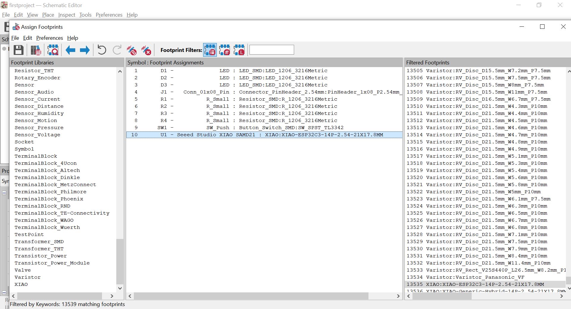

After completing all the steps and tasks, the output of my design is based on the XIao board.
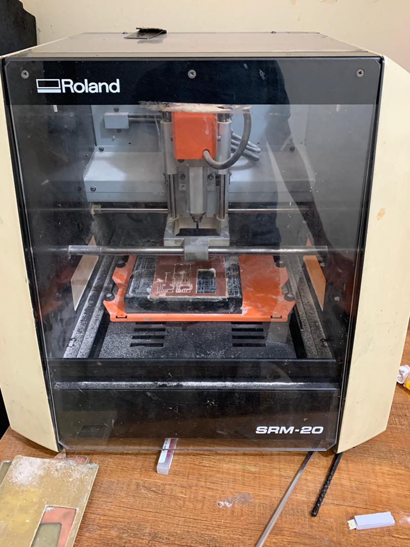
PCB production
After exporting the file from the Kicard software, here the process to export the svg File
that can be used in pcb fabmono.
Go to File => export => select SVG file
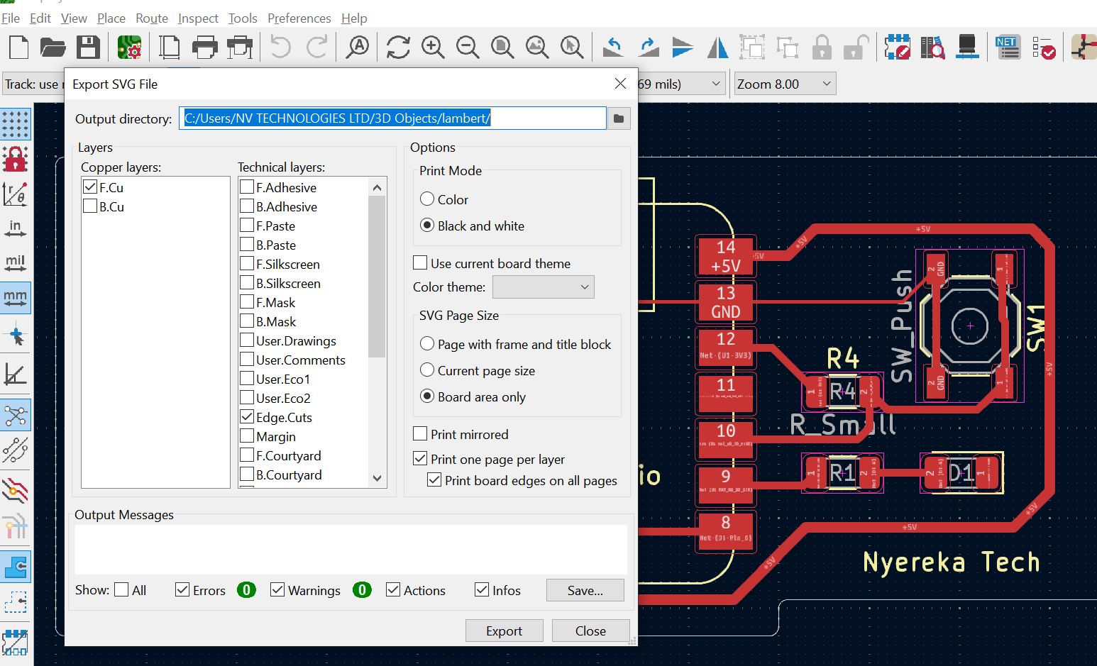
Here you can click on Export and get the file you can insert in MODs fab website in order to get the image to insert in monofab machine. Follow the steps on how to insert if in my week 4.
PCB printing Video
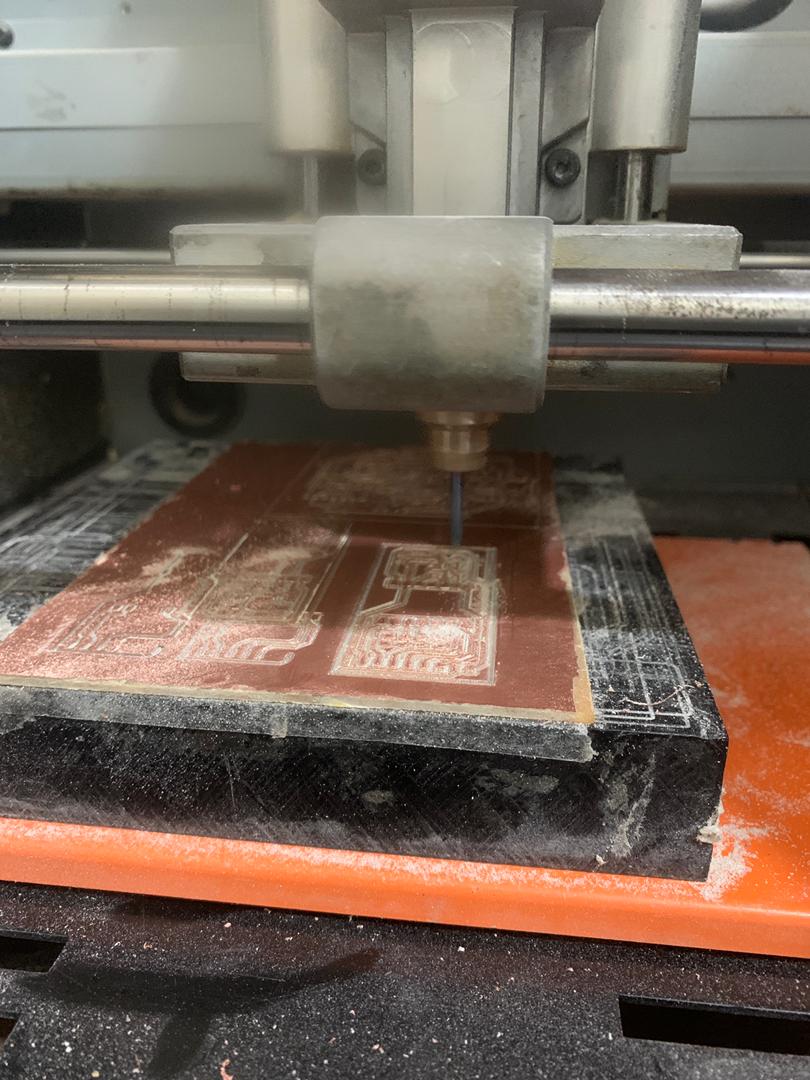
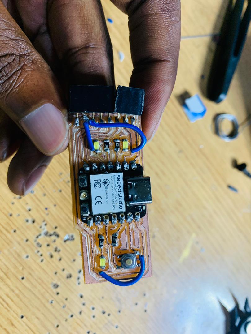
After printing the PCB I found that I made mistake to forgot to connect the lEDs to the ground , so that I connect my LEDs to the graound with wires as you see on the final soldered boards
Programming my PCB
I loaded the code to controll the LEDs attached to the PCB
Code
                        const int buttonPin = D1;  // the number of the pushbutton pin
                        const int ledPin1 = D0;    // the number of the LED1 pin
                        const int ledPin2 = D7;    // the number of the LED2 pin

                        // variables will change:
                        int buttonState = 0;  // variable for reading the pushbutton status

                        void setup() {
                          // initialize the LED pin as an output:
                          pinMode(ledPin1, OUTPUT);
                          pinMode(ledPin2, OUTPUT);
                          // initialize the pushbutton pin as an input:
                          pinMode(buttonPin, INPUT);
                        }

                        void loop() {
                          // read the state of the pushbutton value:
                          buttonState = digitalRead(buttonPin);

                          // check if the pushbutton is pressed. If it is, the buttonState is HIGH:
                          if (buttonState == HIGH) {
                            // turn LED on:
                            digitalWrite(ledPin1, HIGH);
                            digitalWrite(ledPin2, HIGH);
                          } else {
                            // turn LED off:
                            digitalWrite(ledPin1, LOW);
                            digitalWrite(ledPin2, LOW);
                          }
                        }
Video for output

Download file For KiCad PCB
Click the button below to download file.
Download Image