Electronic Design
Here its our group assigment: Week 8What I learned
- A multimeter is a versatile tool used to measure various electrical quantities such as voltage, current, and resistance. When observing a microcontroller circuit board, you can use the multimeter to measure voltages at different points in the circuit. This helps in verifying that the power supply is functioning correctly and that voltages are within expected ranges.
- An oscilloscope is an instrument used to visualize and analyze the waveform of electronic signals. When examining a microcontroller circuit board, the oscilloscope can be used to observe signals at different points in the circuit. This allows you to see how signals change over time, detect abnormalities or unexpected behavior, and verify the proper operation of various components such as sensors, actuators, or communication interfaces.
Individual assigment
Use an EDA tool to design a development board to interact and communicate with an embedded microcontroller
I used KiCad for designing my board.

KiCad is a free and open-source software suite for electronic design automation (EDA). It allows users to design electronic schematics and printed circuit boards (PCBs) with a comprehensive set of tools. Now, let me walk you through how to use KiCad:
- I started by launching KiCad from my desktop or applications menu.
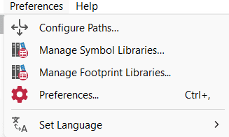
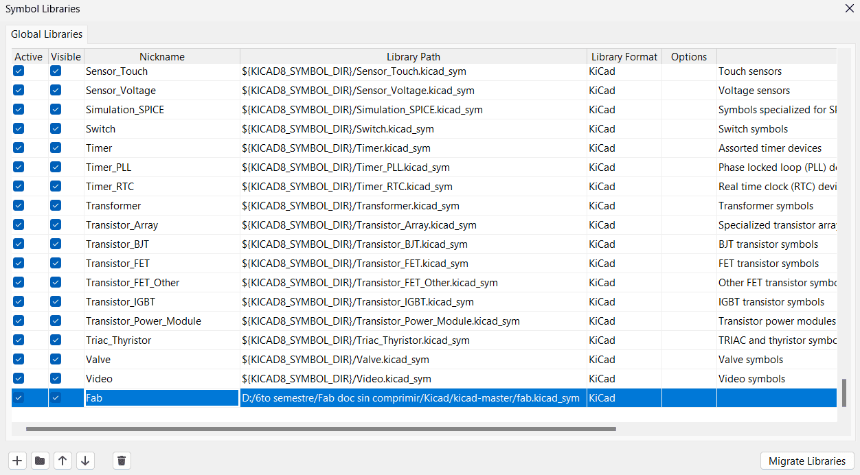
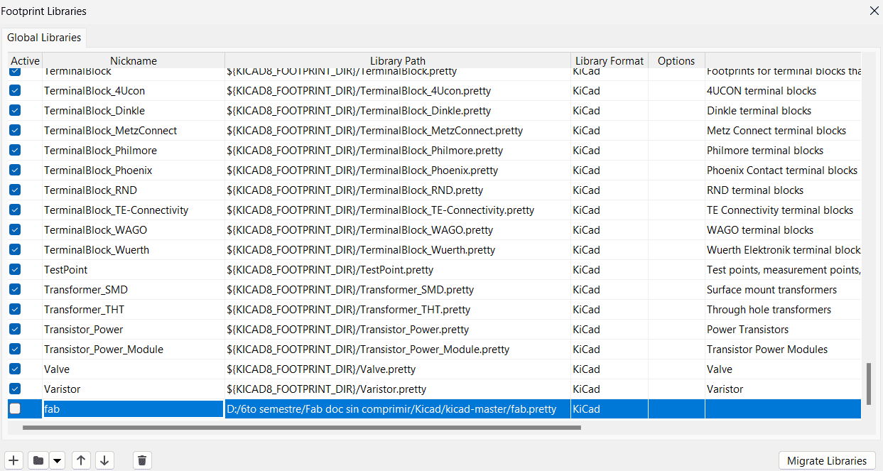
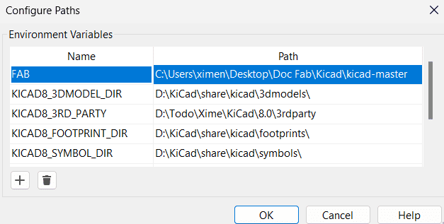
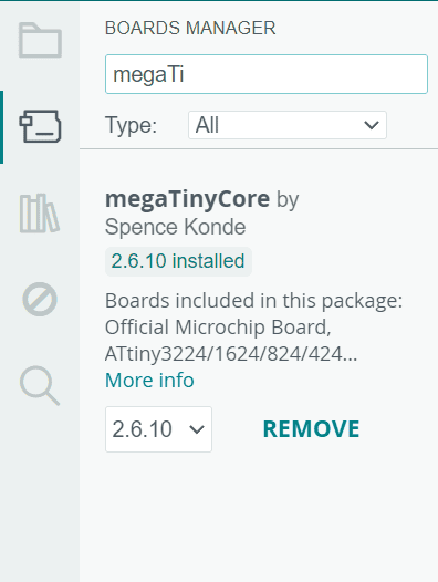
How to add a libraries:
-
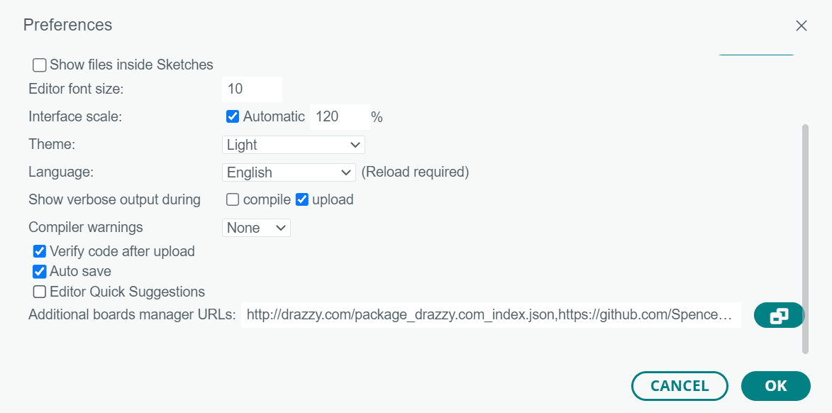
On the upper part of KiCad, you click on the section "Preferences" and there you can add symbols, footprints and paths.
-
When you open each of the section previously mentioned, down below, you can click on the plus button and there you create the docs as shown in the images.
Using KiCad
-
I began by creating a new project or opening an existing one. I navigated to the "File" menu and selected "New Project" or "Open Project" as needed.
-
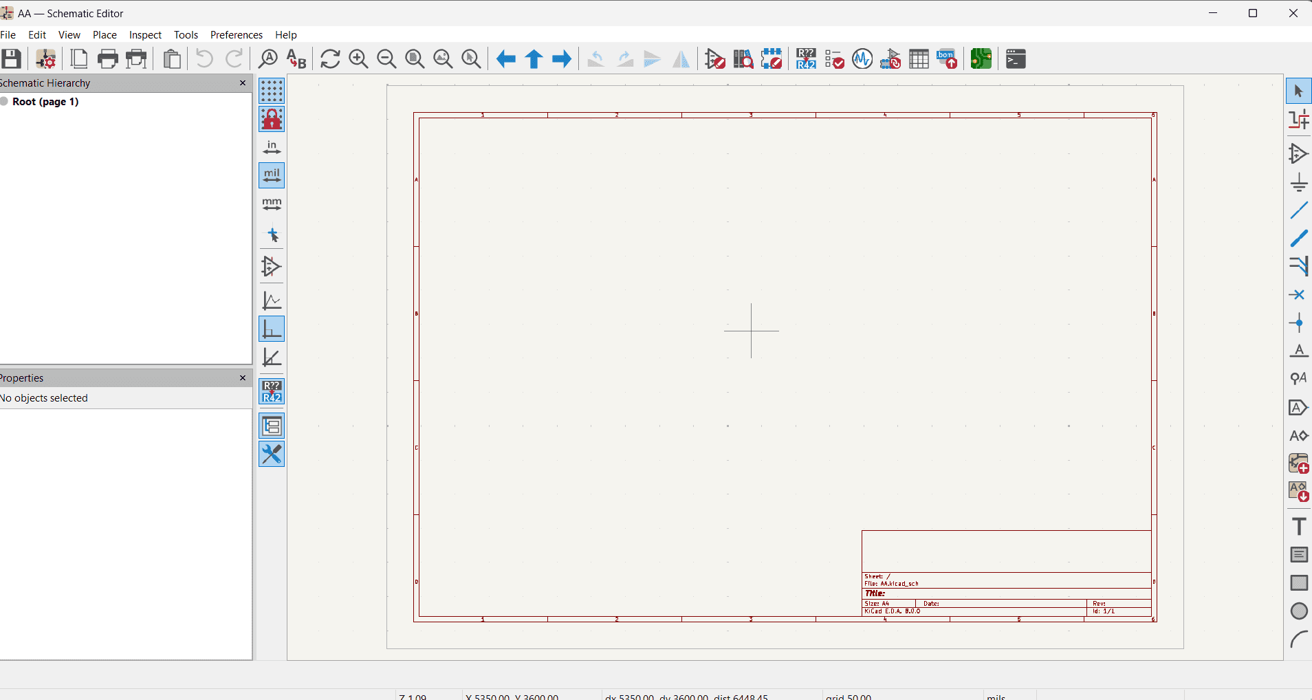
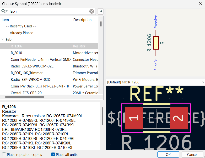
To create a schematic, I clicked on the "Schematic Layout Editor" button. Here, I designed my circuit by placing components from the component library onto the schematic sheet and connecting them with wires. I used tools like "Place Component," "Wire," and "Label" to create a clear and organized schematic.
-
After placing all components, I annotated them to assign unique reference designators automatically. Then, I verified the connections and made any necessary adjustments to ensure correctness.
- Once satisfied with the schematic, I generated a netlist, which was a list of connections between components. I verified that the netlist was error-free before proceeding.
-
I then switched to the PCB Layout Editor to design the physical layout of my circuit board. I imported the netlist generated from the schematic and placed components onto the PCB canvas, arranging them to optimize functionality and minimize signal interference.
-
Using the routing tools provided, I drew traces to connect the pads of components according to the netlist. I ensured that the traces adhered to design rules, such as minimum clearance and trace width, to prevent electrical issues.
-
Once all traces were routed, I performed a design rule check (DRC) to identify and correct any violations. This step ensured the manufacturability and reliability of the PCB design.
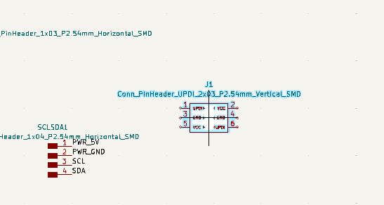
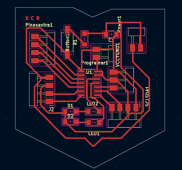
My board
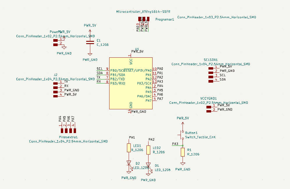
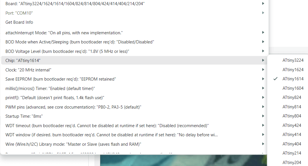
I decided to do use an Attiny1614, which is is a microcontroller chip developed by Microchip Technology as part of their AVR family. It is a low-power, high-performance 8-bit microcontroller with advanced features suitable for various embedded applications.
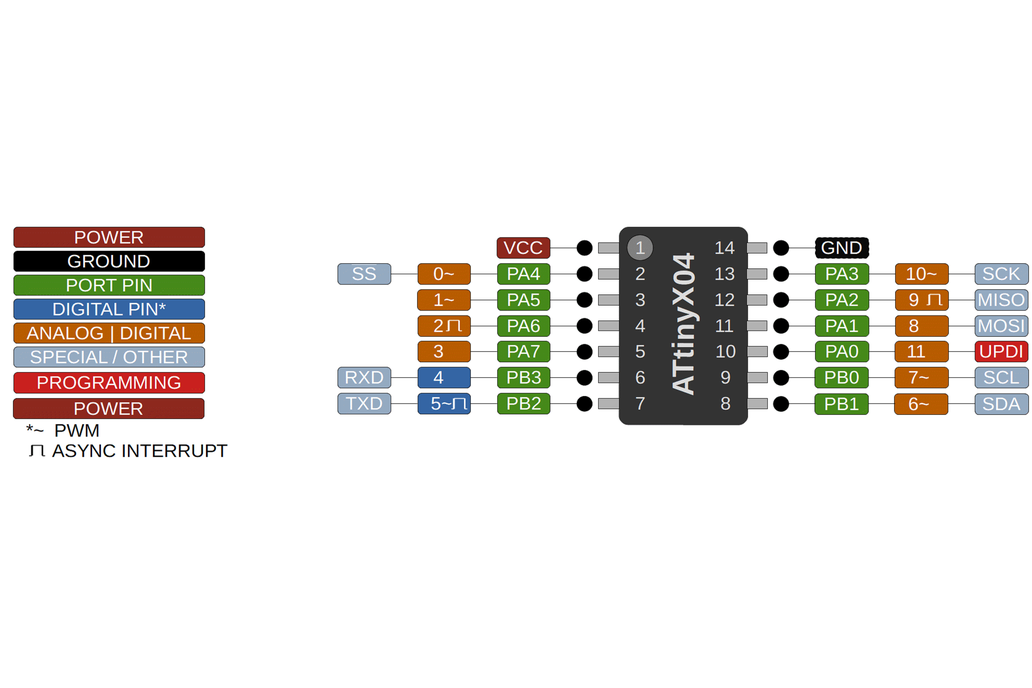
Featuring a 20 MHz CPU core and 16KB of Flash memory, it offers ample processing power and program storage capacity. With integrated peripherals including ADC, timers/counters, USART, SPI, and I2C interfaces, along with up to 20 GPIO pins, it provides flexibility for interfacing with external devices and sensors. Its low-power modes, safety features like brown-out detection and watchdog timer, and built-in security measures ensure reliable operation and data integrity.
This board was specifically designed to provide the necessary pins for programming the sensors required in the final project.
Some key feautures of this board were the following ones:
- I2C Pins (SDA, SCL): For communication with I2C devices such as sensors.
- UPDI Pins (Unified Program and Debug Interface): The three pins necessary to program the board with UPDI
- VCC and GND Sources: Two sets of pins for power and ground.
- TX and RX Pins: For serial communication, useful for debugging and communication with other devices.
- Extra Pins: Available for additional connections, customizable to the project's needs.
- Two LEDs: For visual status indicators.
- Button: For manual interaction or board control.
Here are the steps I followed:
-
Insert the necessary components I explained above:

-
Insert the necesary pins for the feautures I wanted to add.
-
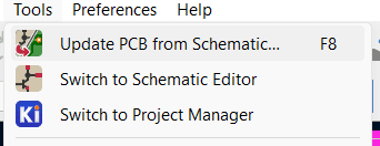
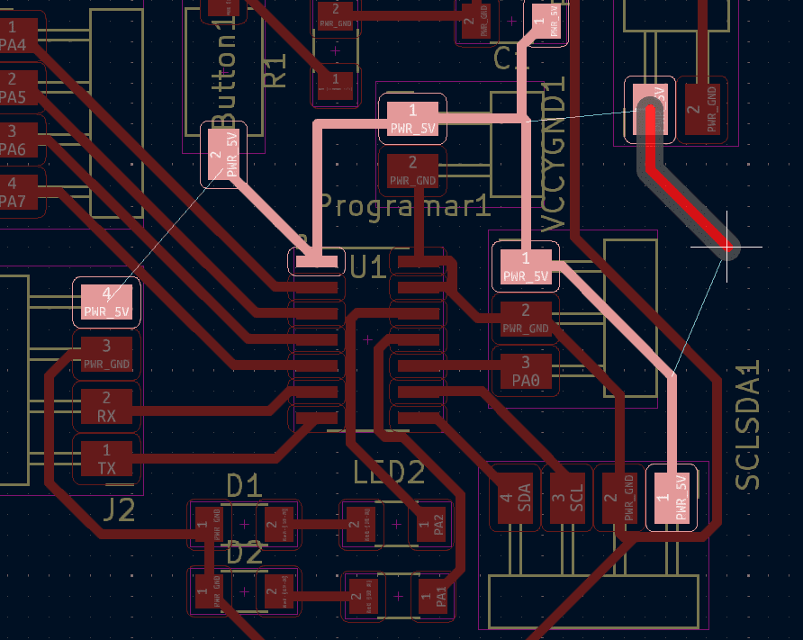
Then I updated the PCB from the squematic I finished.
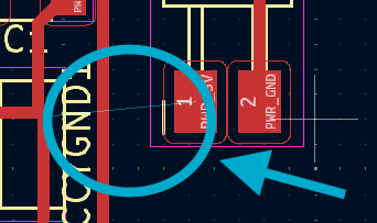
- Now on the layer of F.Cu you need to do the following step.
-
When you do that, some blue lines should appear, showing you what you need to connect with:
-
Make sure to select this tool so you can join all the parts:

-
Once you select that tool the program will automatically show you were to connect it.
-
Then on the layer of the Margin, select thsi tool so you can do the outline:
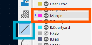
-
It should look something like this:
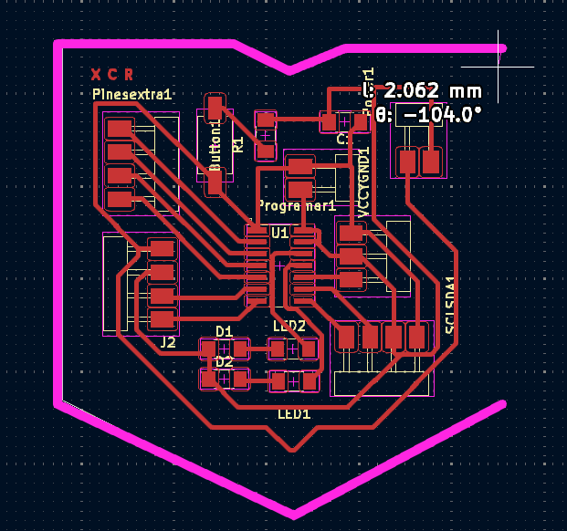
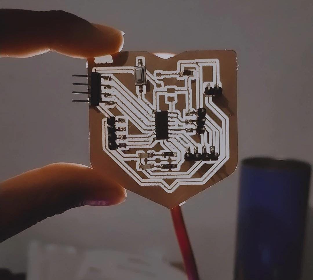
My board
Using the machine
I followed the same steps as in the Week 4| Quantity | Material |
|---|---|
| 1 | Attiny1614 |
| 1 | Capacitor |
| 2 | Smd white Leds |
| 2 | Resistor of 1k |
| 1 | Resistor of 2k |
| - | Pines |
After solding
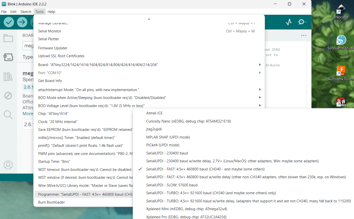
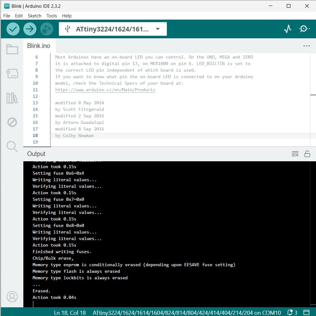
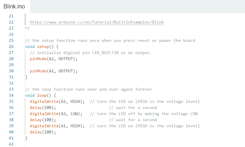
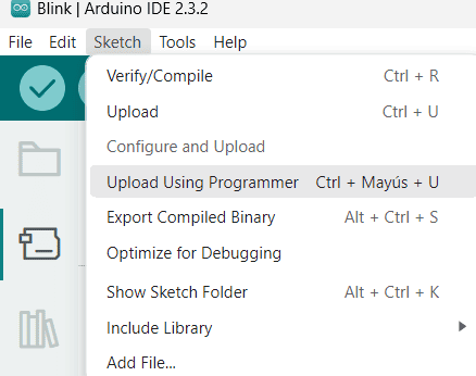
Programing it
I followed the following tutorial from Quentorres, but with some modifications.
https://gitlab.fabcloud.org/pub/programmers/quentorres
- To flash the board and make it ready for use as a programmer, the easiest is to install the uf2 file available here
- Connect your board to a computer via a USB cable. Press the button labeled "B", then hold it pressed while pressing the button labeled "R". You can then release both buttons, and the rp2040 will enter its reset mode.
- Download the uf2 firmware file from here, and place it on the empty hard drive that showed up after step 1. After the file transfer, the board will automatically reset.
- With ARDUINO, you have to first install the Fab SAM core
- Here is the tutorial of how to install it: https://gitlab.cba.mit.edu/quentinbolsee/Arduino-SAM-tutorial/
Flashing a UPDI target
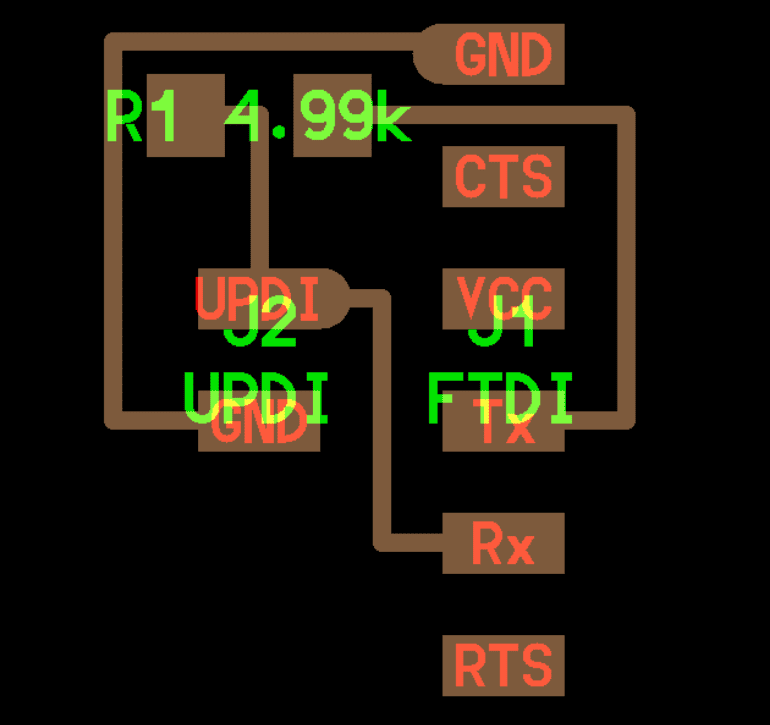
Here is the small pcb conector I made, following those specifcations:
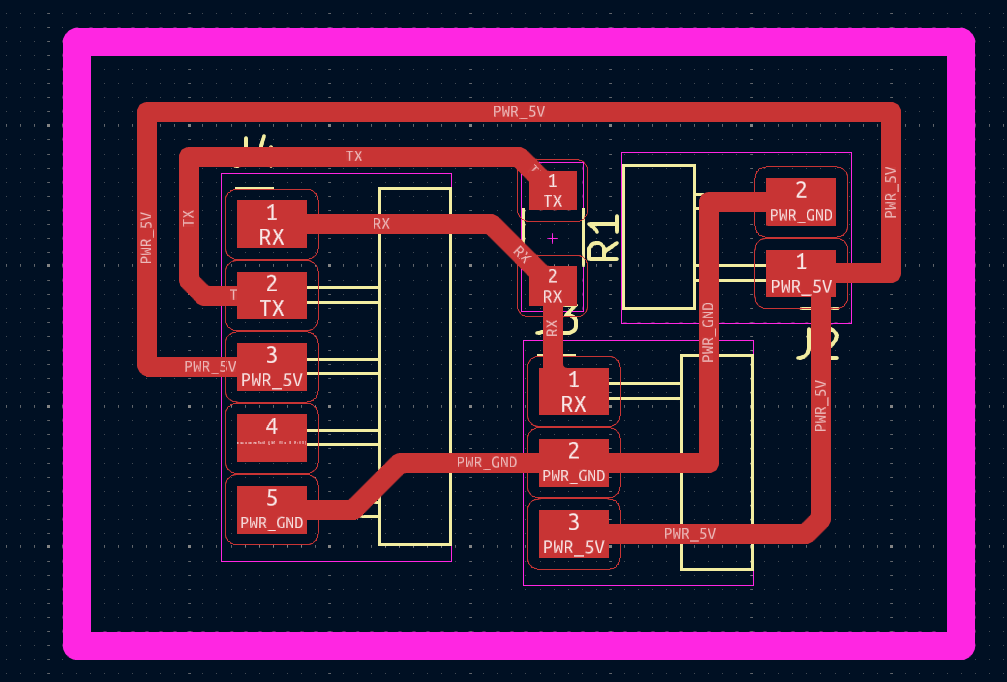

Update: I had some problems solding this pcb, that's why it kinda looks bad, because some traces became really thin and difficult to mantain stable, I didn't wanted to re do this PCB , because in the following weeks I wanted to make the same board but with some design changes that would make easier to use it in different assigments.
Don't make the same mistakes as me...
| Mistake | Solution |
|---|---|
| The errors I encountered were primarily due to thinner traces on my PCB, making soldering more challenging | The solution to this issue is either to increase the minimum trace width or add thicker traces where necessary. |
| Another problem was the lack of a direct connection with the UPDI interface, requiring the use of a protoboard for programming. | To address this, I am currently developing a mini board that will provide easy access to these connections. |
| Lastly, when using cables, slight disconnections during bootloader running caused errors. | To mitigate this, I soldered the cables to ensure they remained secure and stable during operation. |
Documents