8. Electronics Design
On this week we worked on creating a PCB from scratch. This task was kind of difficult but interesting.
The group assignment
Here is the group assignment task where we learn together.
Starting with designing
For this task, we watched on the global class different types of electronics design software, although some of them are a good option, I decided to go with Kicad. On the local class we reviewed Fusion360, Kicad and others...
KiCad is an application to create PCB's. KiCad's Schematic Editor supports everything from the most basic schematic to a complex hierarchical design with hundreds of sheets. KiCad's PCB Editor is approachable enough to make your first PCB design easy, and powerful enough for complex modern designs. A powerful interactive router and improved visualization and selection tools make layout tasks easier than ever. For more info and download click here.
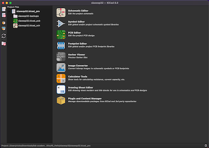
Starting with KiCad we have the main menu:
All the components that we're going to use need a "footprint", for this we need to install the fab library of components, same that we have on the local lab. The next steps are requiered in order to install correctly the library:
1. Download the library: Download from this page the fab library of components. Then decompress the file to use it.
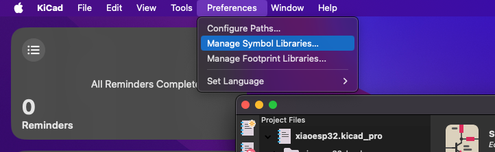
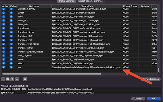
2. Open Symbol library:On the symbol library manager we need to create an empty row, then name it with fab and finally link the path to the fab.kicad_sym
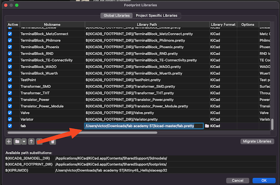
3. Configure the footprints: To configure the footprints it's need to open the "Manage Footprint Libraries" and add in an empty row calling it fab the link to fab.pretty.
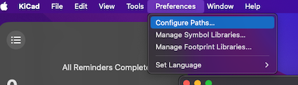
4. Configure paths: The next step is to configure the paths, this by creating again an empty row, name it FAB with uppercase and link it to the complete file.
Start creating on KiCad
It's time to create on KiCad. This first step is to decide what we're going to do. For this I decided to go with a XIAO ESP32 because it is going to be useful for my final project. In this case I want my PCB to have a lot of pin outs in order to make this PCB useful for the final project and week tasks.
The materials that I want this PCB to have and I need to solder are going to be:
- XIAO ESP32c3: the controller.
- 2 x Tactile switch (buttons): to test only certain things.
- 2 x led 1206: too for testing certain things and as indicators.
- 1 x 0.1 uF capacitor: to clear signal at 5v.
- 1 x 4 set pin header out: this is going to have all the UART communication requirements (Tx, Rx, VCC and GND).
- 2 x 3 set pin header out: One of the for only VCC's and GND and the other one for outputs (D10, D9, D8).
- 1 x 2 set pin header out: For D5 and D4. This are going to work for the SDA and SCL.
Now let's create the schematic.
To create the schematic, we need to start adding elements:
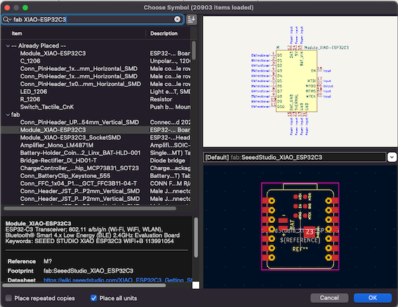
Then we need to search the element we want to add. Because we have the fab library, we search with "fab ELEMENT TO SEARCH", as the next example:
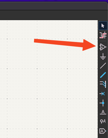
After we click ok we can add that element to the schematic canvas. We can add GND's and VCC's, for this we use the next icon:
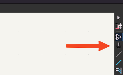
After we click ok we can add that element to the schematic canvas. We can add GND's and VCC's, for this we use the next icon:
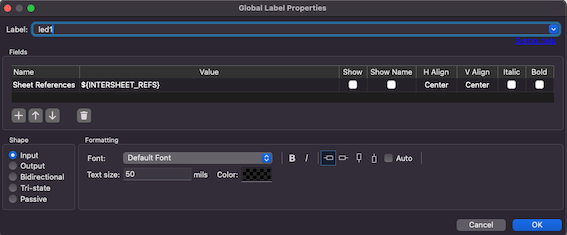
We can create labels, this in order to not use wire everywhere. The labels work as a wire and it looks clean when adding elements to the canvas.
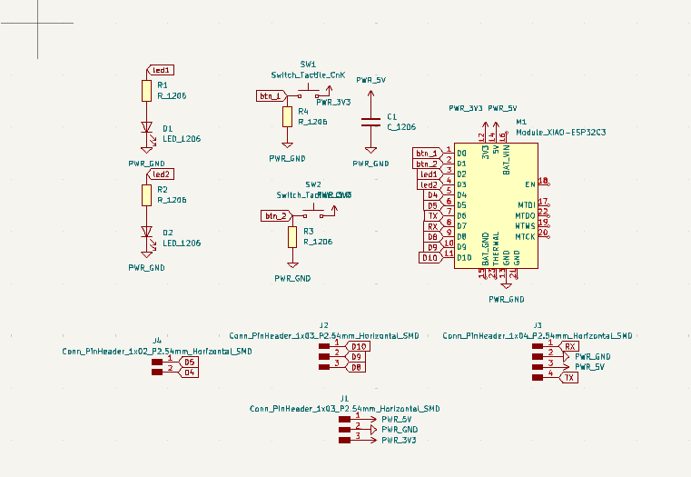
After adding all the elements mentioned before, we got this schematic:
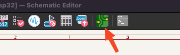
Now it's time to the PCB Editor. For this we click on the next icon:
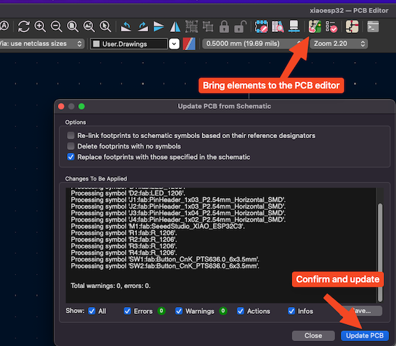
Then we need to import all from the schematic, so we click on the icon and import them as I show below:
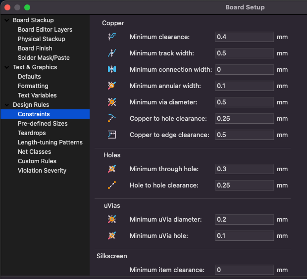
Time to set constraints. This is important in order the give a considerable space between wires and make them with a considerable size:
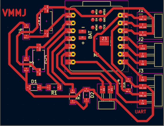
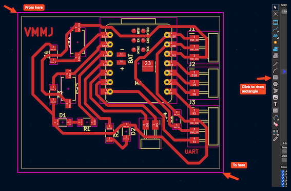
After that the most difficult part is the next, make everything to be in order and not to cross wires. After some hours, this was my result:
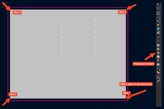
Now lets draw the borders for cutting:
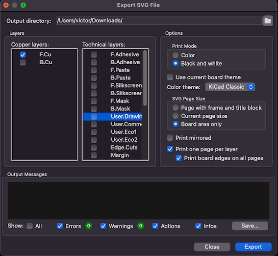
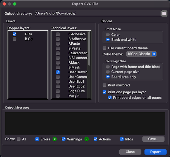
Almost done but we need to export the traces and the cuts. The traces are going to be all the wires. The cut is going to be what the milling machine is going to cut.
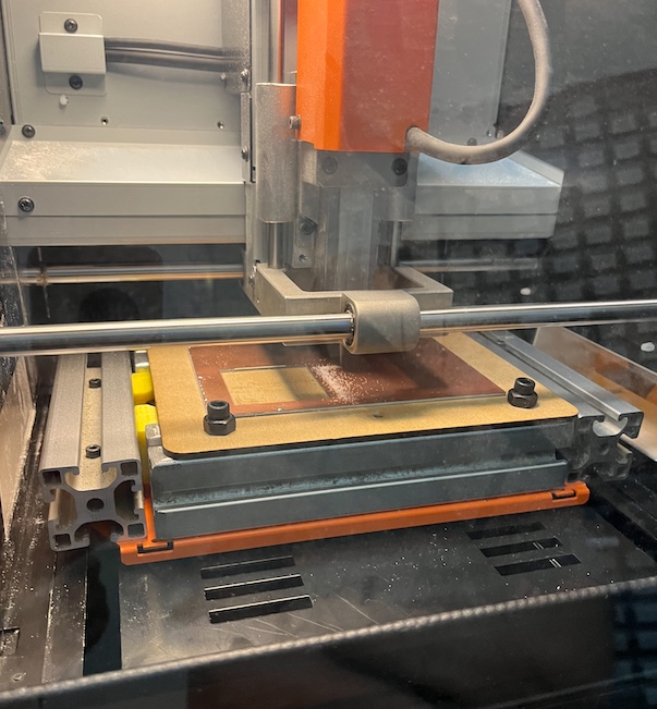
Time to use the milling machine
As we worked on the electronics production task, we are going to do almost the same for the traces and the cut.
The first step on this is to transform the .svg on the mods project page with the parameters shown on the electronics production task. (Which are coordinates on 0, selecting if traces or cut, machine, if needed change the color of the image and export.
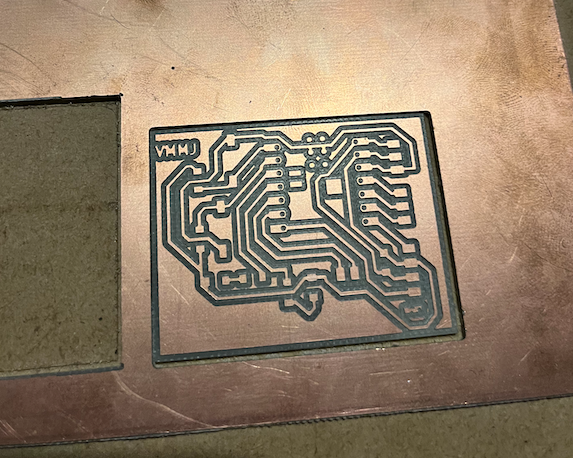
We got this:
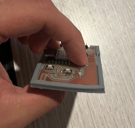
Checking if the XIAO is going to fit:
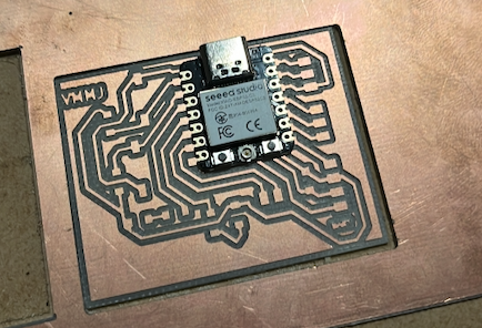
Before solder, it's important to consider that we need to add isolation tape on back of the XIAO. This is needed to make the PCB work. With the isolation tape, the footprint of the XIAO doesn't matter on this circuit.

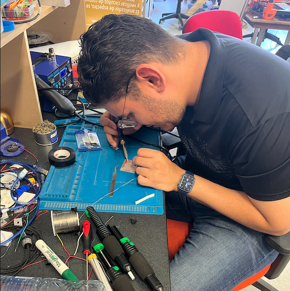
Let's solder, this is me soldering every component that I mentioned before:
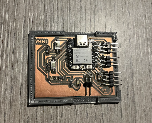
An finally we got:
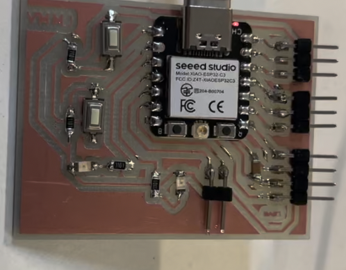
Let's check if it's working, so to check this I made a program that uses the two buttons and the two leds. It seems working!!!!
Here is the arduino Code:
const int buttonPin = 2;  // the pin that the pushbutton is attached to
const int buttonPin2 = 3;  // the pin that the pushbutton is attached to
const int ledPin1 = 4;    // the pin that the first LED is attached to
const int ledPin2 = 5;    // the pin that the second LED is attached to

int buttonState = 0;      // variable for reading the pushbutton status
int buttonState2 = 0;

void setup() {
    pinMode(ledPin1, OUTPUT);  // initialize the LED pin as an output
    pinMode(ledPin2, OUTPUT);  // initialize the LED pin as an output
    pinMode(buttonPin, INPUT); // initialize the pushbutton pin as an input
    pinMode(buttonPin2, INPUT); // initialize the pushbutton pin as an input
}

void loop() {
    // read the state of the pushbutton value
    buttonState = digitalRead(buttonPin);
    buttonState2 = digitalRead(buttonPin2);

    // check if the pushbutton is pressed
    if (buttonState == HIGH) {
    // turn on the LED connected to pin
    digitalWrite(ledPin1, HIGH);
    // turn off the LED connected to pin
    digitalWrite(ledPin2, LOW);
    } else if(buttonState2 == HIGH){
    digitalWrite(ledPin2, LOW);

    }else {
    // turn off the LED connected to pin 4
    digitalWrite(ledPin1, LOW);
    // turn on the LED connected to pin 5
    digitalWrite(ledPin2, HIGH);
    }
}
After that I decided go for the extra credit and make it more safe, so I created the cover. I designed this on Fusion360 and printed it on the 3D printer.
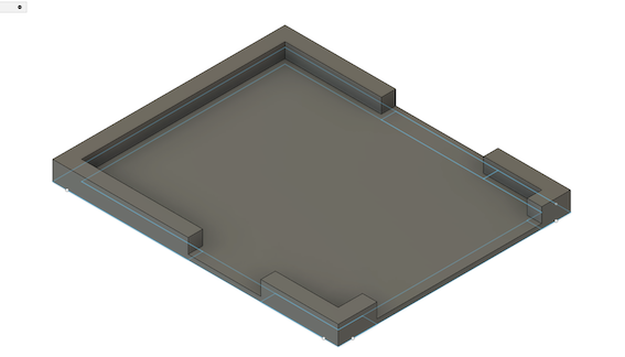
After printing and inserting the PCB, we got this: