Electronics production
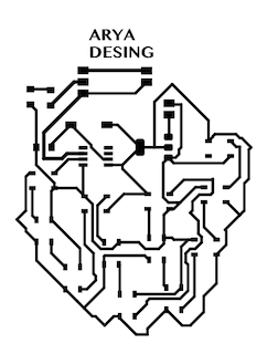
For this assignment, I decided to create a heart-shaped PCB to experiment with a variety of components and create my own electronic circuit design
Team Practice
Here its the link of our team practice.
COMPONENTS LIST
| Material | |
|---|---|
| Microcontroller | Attiny 412 |
| Neopixel | 12 pieces |
| Button | 1 |
| Resistor | 1002 k |
| LED | Orange color |
| Resistor | 1001 k |
| Regulator | AMS1117 |
| PINS | 5 |
This components and the Xiao from the assigment of the week04 are the components that I have used for this electronic desing.
KiCad PCB Design
Step 1
For my schematic design, I used the KiCad program to create my circuit.
Step 2
To do this, I downloaded the KiCad program.

Step 3
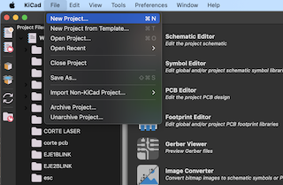
Open a new project, assign a name to the project, and save it in the desired location.
Step 4
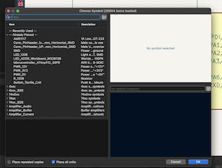
With the components ready, I add them to the program by selecting the letter "A."
Step 5
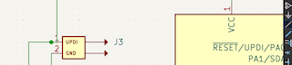
I connect them with a "wire" by pressing the W key, grounding the necessary ones and connecting the required ones to 5V voltage.
Step 6
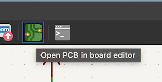
Once the connections are ready, I save the schematic, and in the upper part, I select the PCB button, where I will generate my entire design for etching and cutting.
PCB Design
The PCB part helped me create the electronic desing before sending it for actual cutting, allowing me to identify any potential errors or issues.
Step 1
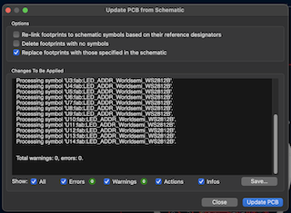
Within the new PCB tab, we go to "Tools" and select "Update PCB from Schematic," a box appears with the specifications where we check that there are no errors and click "Update PCB."
Step 2
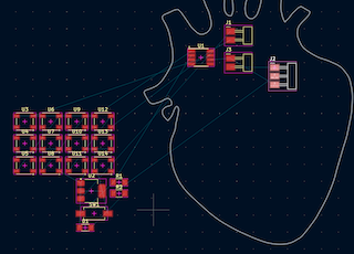
All our components will appear together, and with a click, we place them in the middle of our page.
Step 3
There we will begin to arrange them based on the lines that connect them to do it as best as possible and avoid connection errors or complications.
Step 4
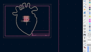
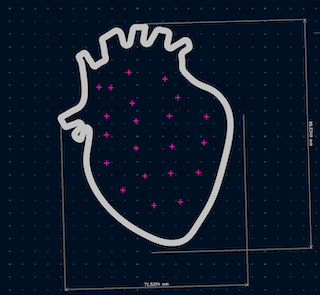
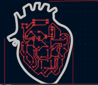
In this case, I decided to first put the outline of the shape of my heart that I previously drew in Procreate.
Step 5
This is imported as a graphic and placed in the desired location, in this case, it is placed on the "USER DRAWINGS" layer.
Step 6
I gave it the measure 8.7 x 7.3 mm since that space would fit perfectly on my cutting board.
Step 7
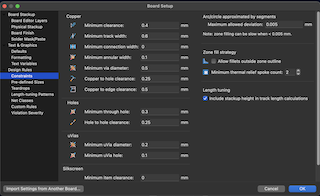
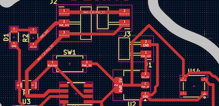
With the base shape, I arranged my components and gave a thickness to my track of 0.6mm and a separation between each of 0.4mm to maintain order and good track thickness.
Step 8
I followed the shape of the heart with the components until connecting each one of them.
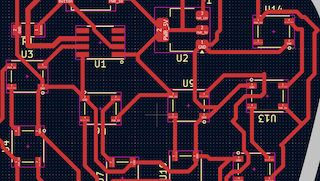
Step 9
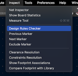
When my circuit was ready, I verified all the connections, went to "iINSPECT," and selected "Design rules checker," where it automatically presents possible connection errors and warnings.
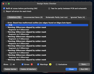
Step 10
I corrected the error, which basically was that my outline touched some tracks and that some touched the components, and the warnings were because of the component numbers, which I simply turned off the layer and finished my circuit.
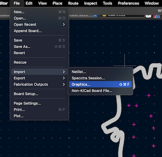
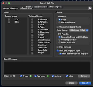
Step 11
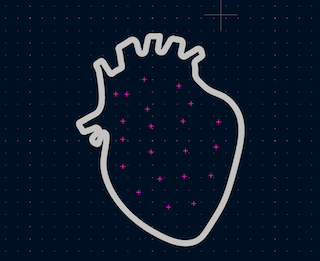
Once ready, I exported it in SVG format, from there, I select F.Cu as the layer where all the components are, this will be the etching of my board, and I export it.
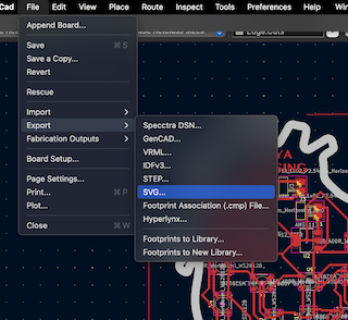
Step 12
Then I do the same but in this case, I select the User drawing layer, which is the layer that has my plate cutting contour, and I export it as SVG.

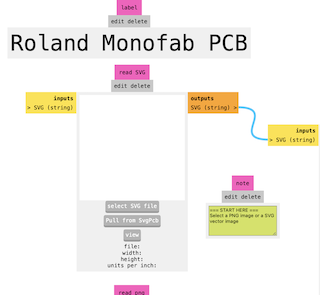
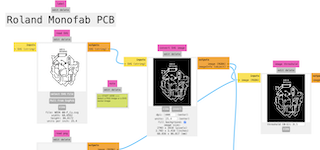
ROLAND PCB
Step 1
First, open the "modsproject" page, where the interaction between the program and what we want to cut and engrave takes place to obtain the file we'll send to the SRM-20 cutter.
Step 2
Within the "Mods" program, right-click to access the menu, select "programs," then "open program," and choose the machine in this case, a "mill 2D PCB."


Step 3
Once in the program, navigate to the area where I would add my SVG file, in this case, the engraving of the PCB.
Step 4
With the file inside, I proceeded to adjust some parameters.
Step 5
The first parameter I checked was in the "set PCB default" section, ensuring that "mill traces" was set to 1/64.
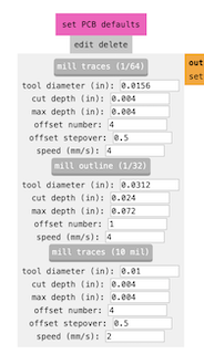
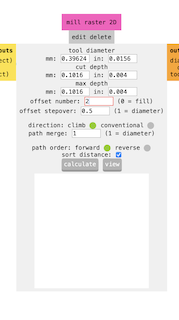
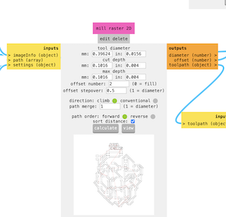
Step 6
I then moved to the "mill raster 2D" section and changed the offset number to Select 2 offsets so that the part that engraves the plate can pass enough to engrave without any issues and without drilling it.
Step 7
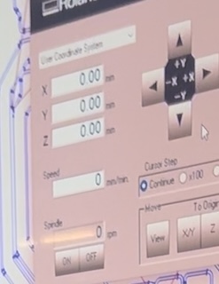
Next, I went to "Roland SRM-20 milling machine" and set the X, Y, Z parameters to 0 to mark an origin point.
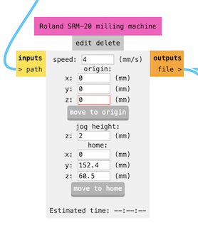
Step 8
I went to Inputs and Outputs, turning it on.
Step 9
Returning to the "mill raster 2D" section, I clicked the "calculate" button to generate the document for the machine and downloaded it in “.rml”format.
Step 10
I did the same but now with the cutting one and saved the format in ".rml".
Step 11
With both formats ready, I went to the Roland program.
Step 12
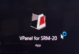
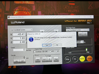
Once adjusted, I returned to the computer, opened the "VPanel for SMR-20" program, closed the machine door, and it calibrated automatically.
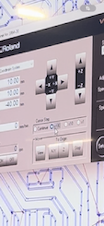
Step 13
Using the program arrows, I positioned the engraving tip in the lower-left corner, marking X, Y parameters at 0 as the origin, and then set the Z point using a metric M2 key.
Step 14
I changed the cursor to "x100" in the program to lower the Z origin slowly, avoiding collision with the piece.
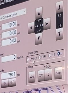
Step 15
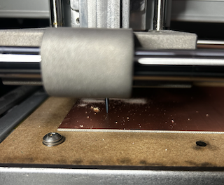
To ensure the Z origin is well-defined, I started the program, waited for the necessary revolutions, and gradually lowered the Z point until it touched the material, marking Z as 0.
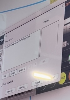
Step 16
Moving to "Cut," I selected "add," added the previously saved file, and then selected "Output."
Step 17
The program automatically started engraving.
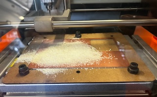
Step 18
After 18 minutes, the piece finished engraving.
Step 19
I did the same process but now with the second contour document.
Step 20
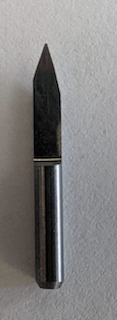
I changed my drill to a cutting drill and recalibrated the Z position with the X, Y movement.
Step 21
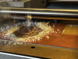
Marked the Z origin again, went to "cut," deleted the previous file, added the new file, and clicked "output." The cutter started descending automatically and cut the board.
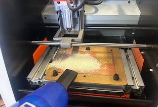
Step 22
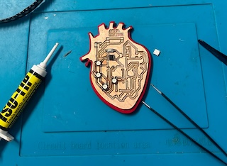
Once finished, I opened the machine door and used a handheld vacuum to clean the dust, leaving the engraved and cut board free.
COMPONENT SOLDERING
To solder my components, I used a soldering iron and solder, although I also needed a heat gun from the soldering station.
Step 1
Based on my previously designed PCB, I positioned my components for soldering without errors.
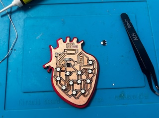
Step 2
I started with the microcontroller, working from the inside out.
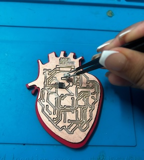
Step 3
In the case of the neopixels, I used solder paste and the heat gun set to 180 degrees to solder them without problems and reinforce them with solder and a soldering iron.
Step 4
And there, the soldering was completed.
BOARD PROGRAMMING
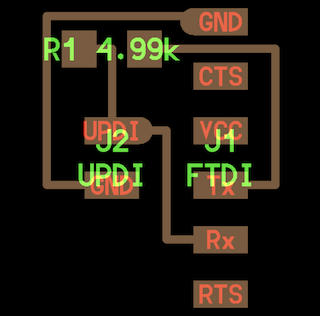
To program my board with my Attiny412 microcontroller, I relied on QuenTorres' UPDI programming.
Step 1
At this point, I realized that an extra board was necessary, which I did not have, so I had to use a protoboard for the time of the assignment to connect my new board with the XIAO RP2040 board that I had previously made.
Step 2
Once the three boards were connected to 5V voltage, ground, to my UPDI and DX, I downloaded Arduino version 1.8 for programming.
Step 3
I downloaded the document from QuenTorres' Fab Academy page.
Step 4
Then, I pressed the R and B buttons on my board with my XIAO simultaneously and released them when connecting it to my computer via my USB-C cable.
Step 5
When my XIAO appeared on the computer, I added the document that would be read by my Attiny 412 to that folder, and it is automatically ready to be used.
Step 6
Its important to say that I used the Arduino 1.8.19 interface, so downlad its important. Similarly, I copied the link with access to the Magatinycore library in Arduino.
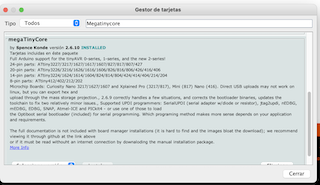
Step 7
I downloaded the MegaTinyCore from Spence Kondo in the Arduino board manager.
Step 8
Then, I selected Tools/Board/Attiny 412.
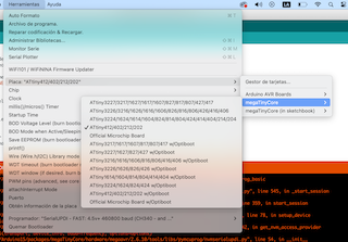
Step 9
I also selected Clock/16 MHZ to load my code onto the boards without any problems.
Step 10
Similarly, I selected Port/SerialUPDI - FAST: 4.5v+ 460800 baud (CH340 - and maybe some others).
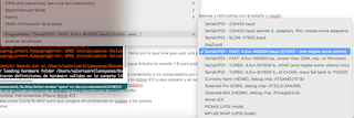
Step 11
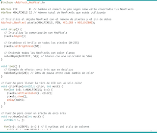
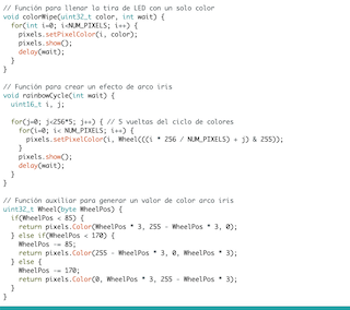
I put a test code to make the neopixels work in a rainbow shape, based on the Attiny412 datasheet to define my pin and neopixels.

FINAL
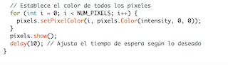
HEARTBEAT SIMULATION EXERCISE
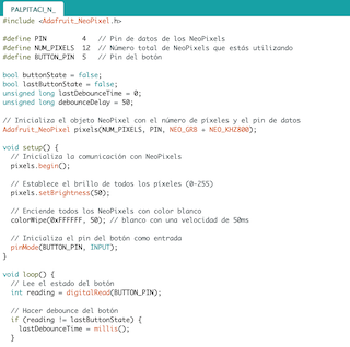
This exercise was the one I wanted to design from the beginning: simulating the heartbeat with neopixels.
Step 1
Basically, I defined my pixels and assigned a color to each, created a loop for the animation with brightness, and defined a timing for them.
Step 2
And there it is, my programming and final design are complete.