8. Electronics design
First of all, in our group webpage (click here), We've included for you the relevant information about a microcontroller circuit board operation using a multimeter and oscilloscope.
For this assignment, I'm going to use Kicad software to design the schematic and the PCB. So, download it (click here) and our FABLab Puebla library that contains a list of the components that we find in the University.
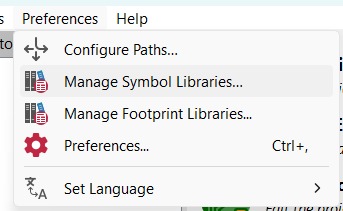
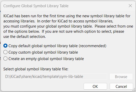
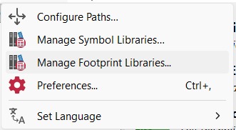
First, in the preferences tab, we'll click on "Manage Symbol Libraries", then a dialog box will appear, and we'll choose the option (recommended).
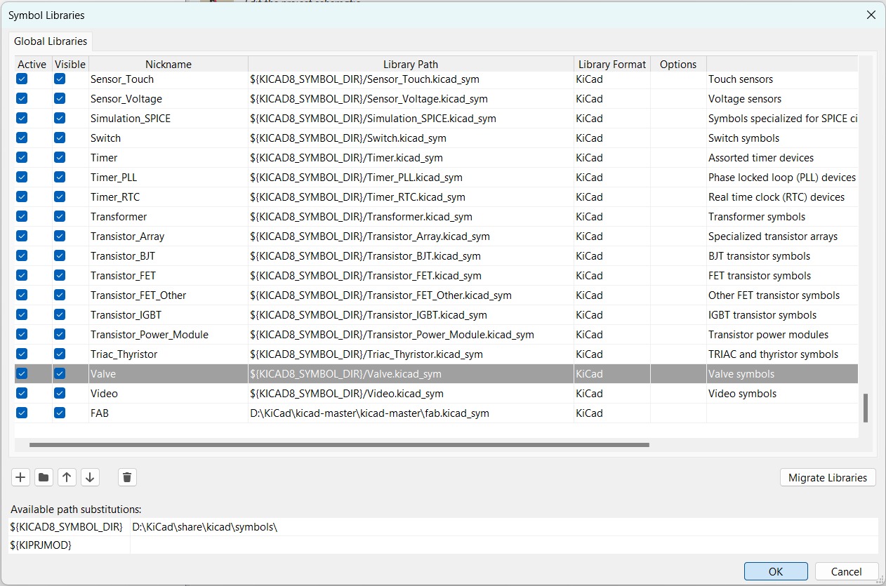
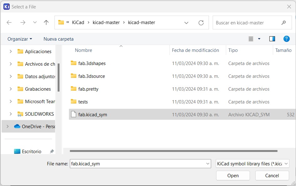
Then, we'll add in uppercase letters the name of our new library, in my case "FAB", and in the folder we downloaded, we'll select the SYM file.
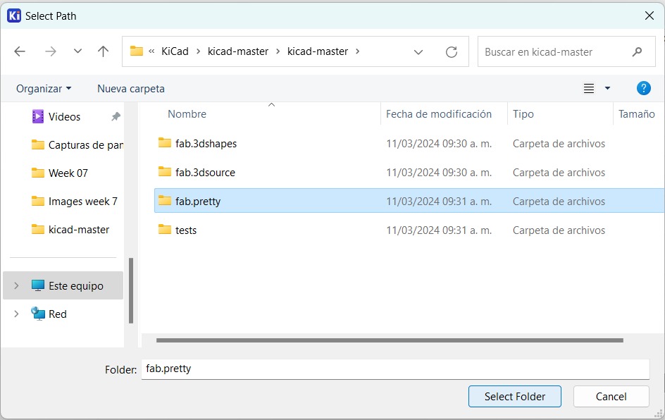
After that, we open the preferences tab again and click on "Manage Footprint Libraries". We create a new one with the name in lowercase letters and select the "fab.pretty" folder.
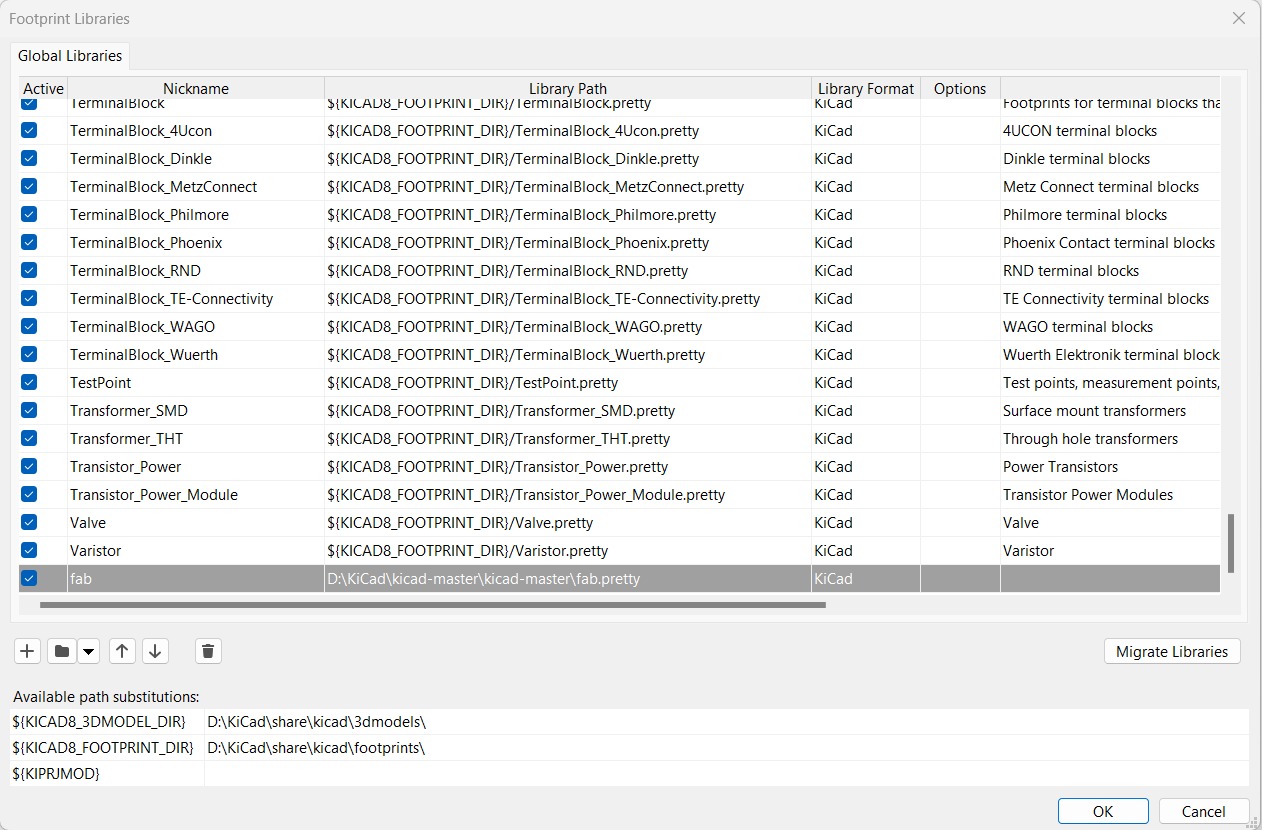
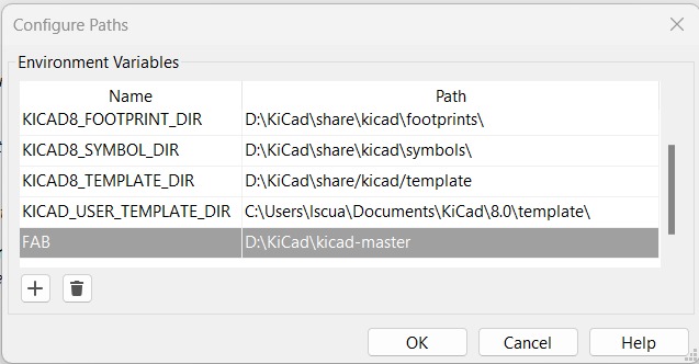
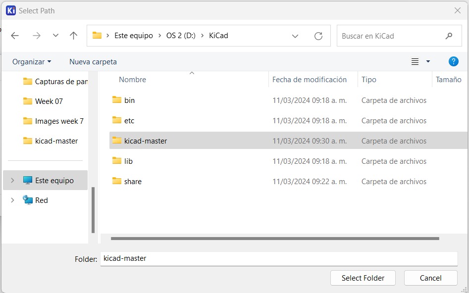
For the paths, we select our library with uppercase letters and the "kicad-master" folder.
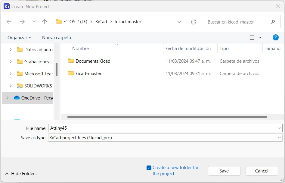
Now, to create a new project, we follow these steps: File - New Project - Create Folder - File name.
Double-click to open the schematic. Here are some commands that will help us to make our circuit more easily:
- A Key - Add symbols
- R key - Rotate
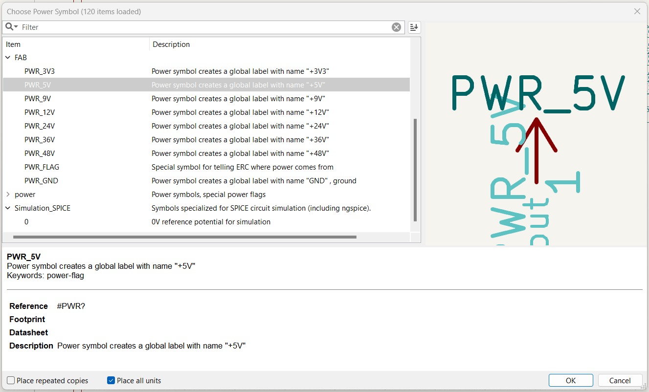
- P -PWR
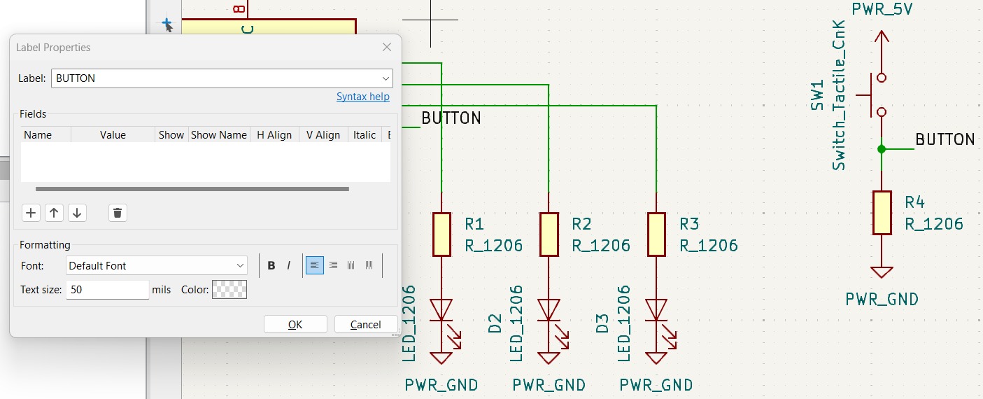
- L - Labels
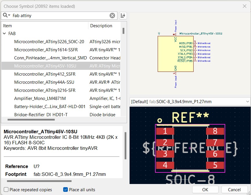
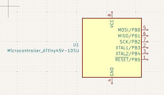
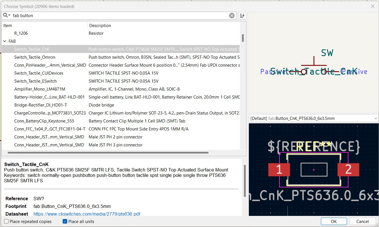
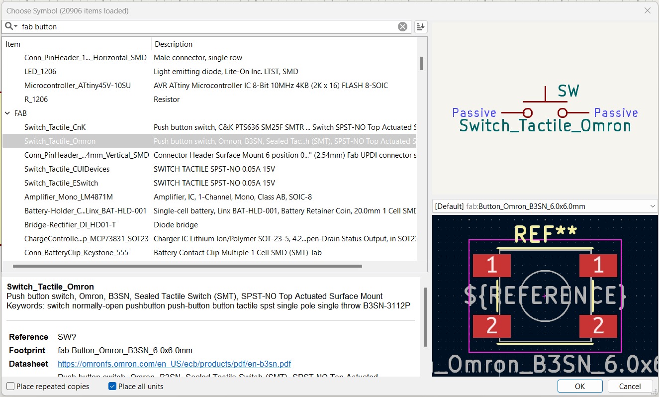
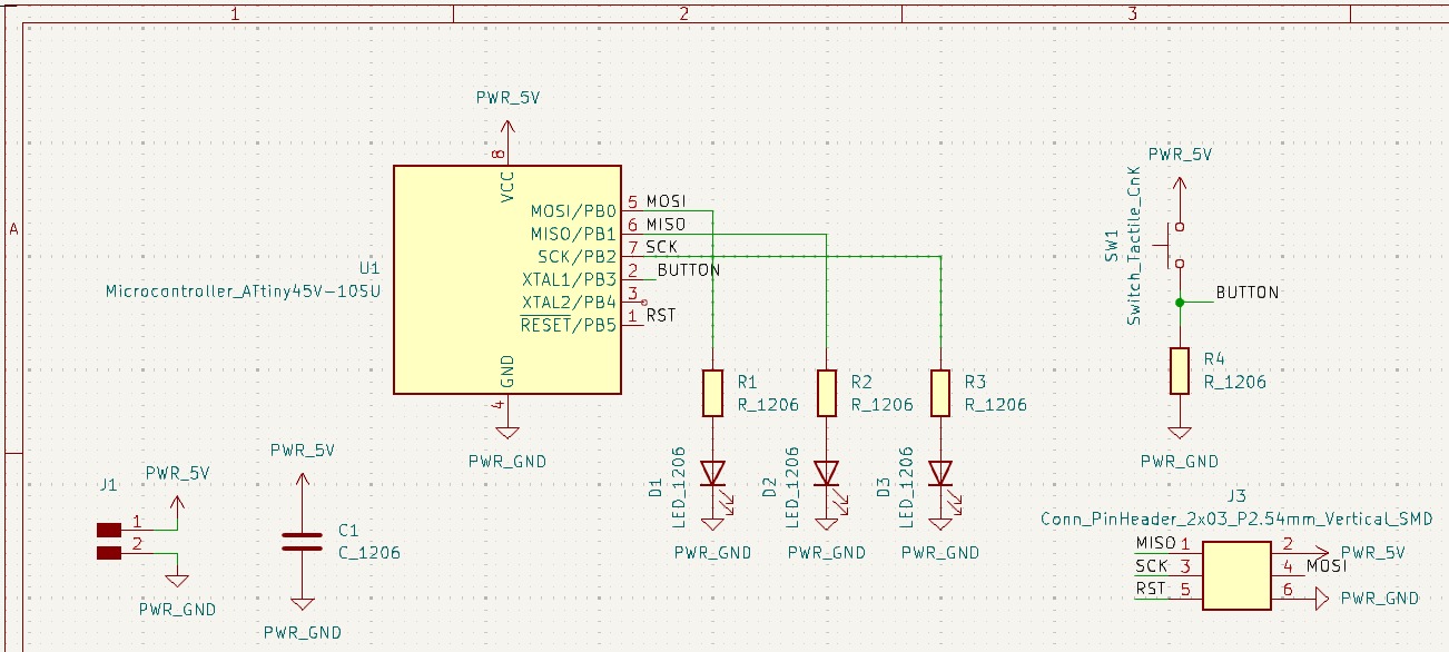
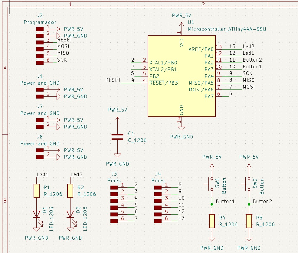
First, we choose the schematic of our MCU by searching for it in the search bar preceded by the word "FAB," which is our library.
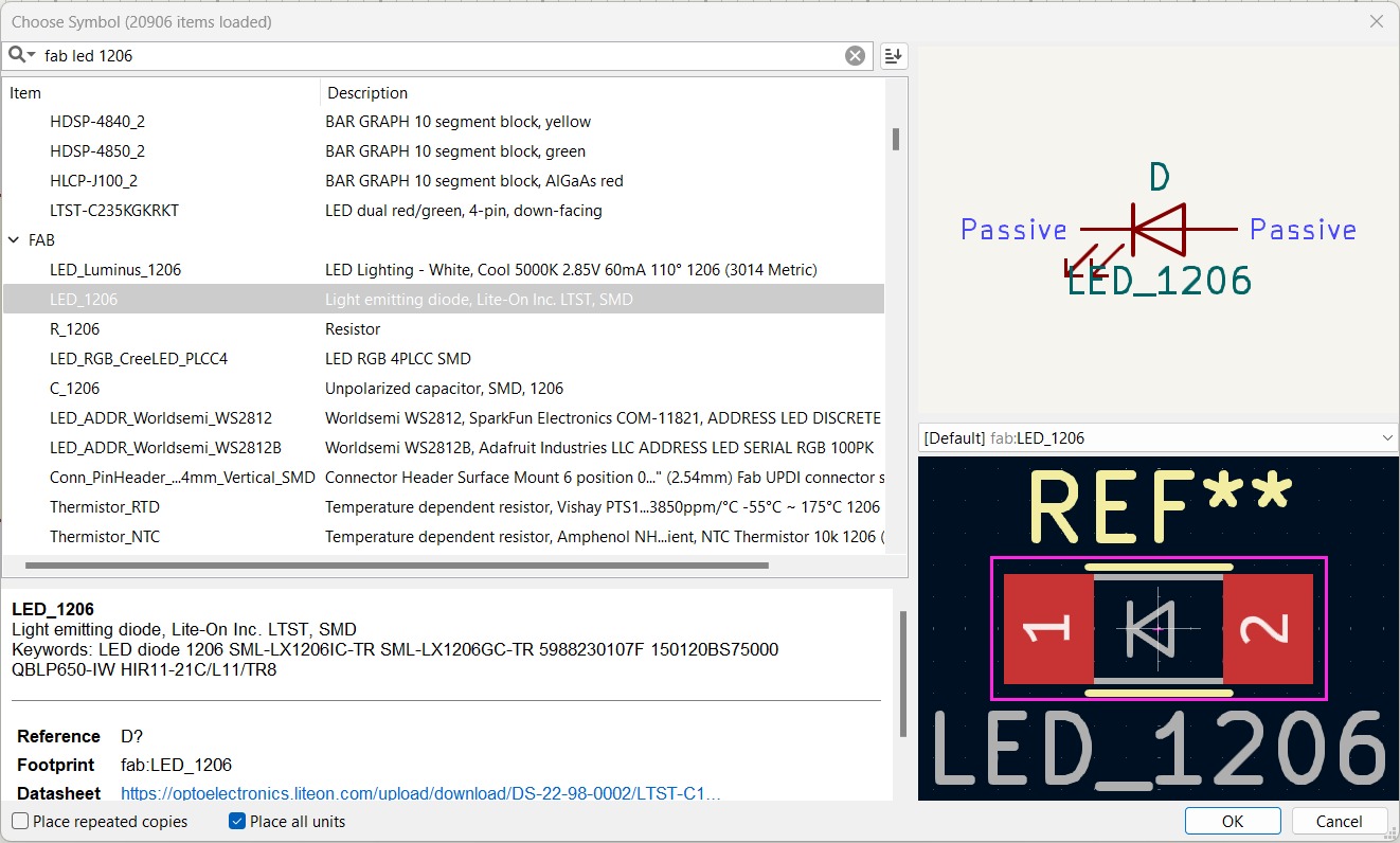
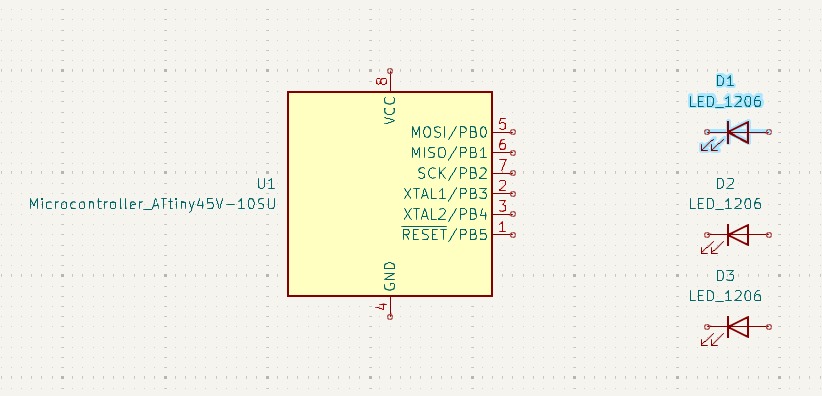
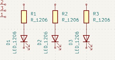
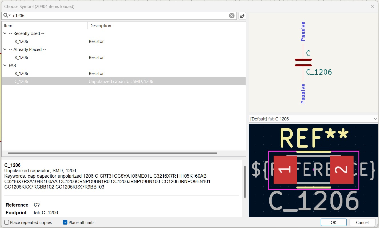
Then, we select the LEDs, preferably using the 1206 size for PCBs. Remember that on the right side, you can see the symbol in the schematic and the footprint of the component.
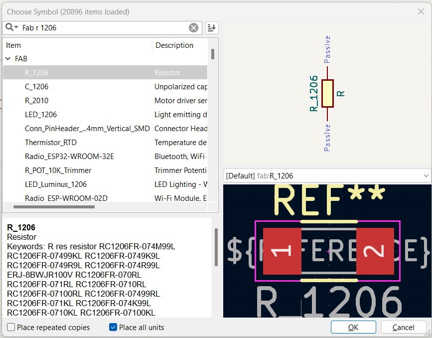
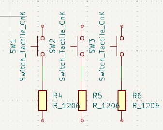
Similarly, we choose the resistors. You can use wire (w) to connect
The buttons may not have the same footprint despite having the same schematic symbol.
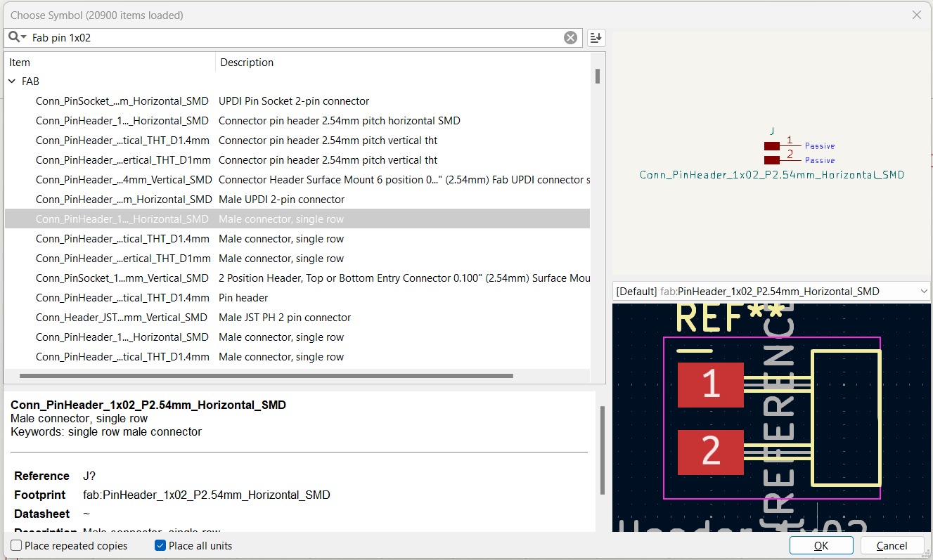
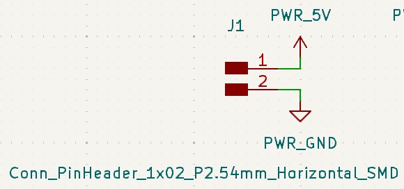
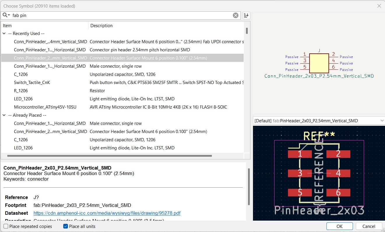
To connect voltage and ground, we use a 1x02 PinHeader with a 2.54 mm pitch, which is equivalent to one-tenth of an inch. Pressing the "P" key allows us to access the voltage and ground elements, which we connect to the pins.
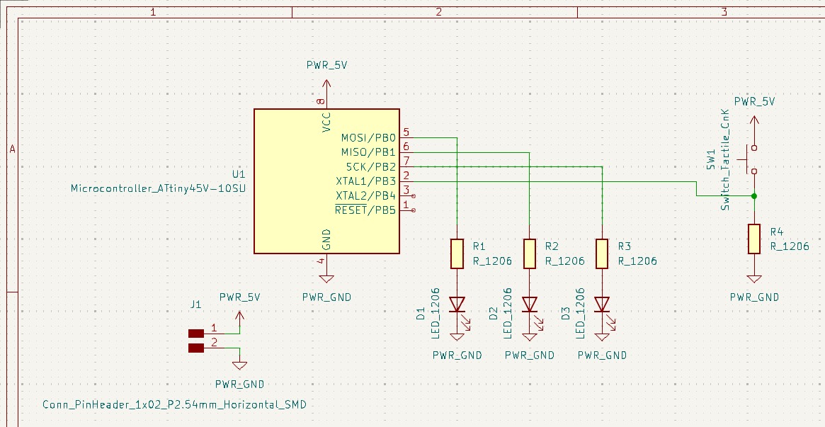
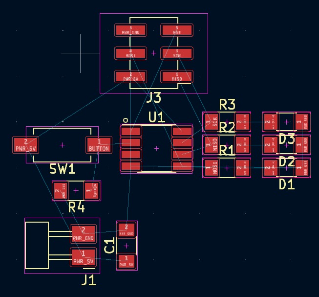
This is the circuit so far.
Pressing the "L" key allows us to place labels, which will enable us to connect each component "invisibly."
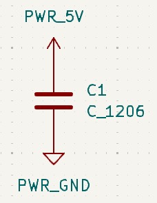
Additionally, it's important not to forget to connect a decoupling capacitor between the pins that will receive power from the source and the MCU.
It's also crucial to place the pins for programming the MCU.
This is a basic schematic for a circuit board.
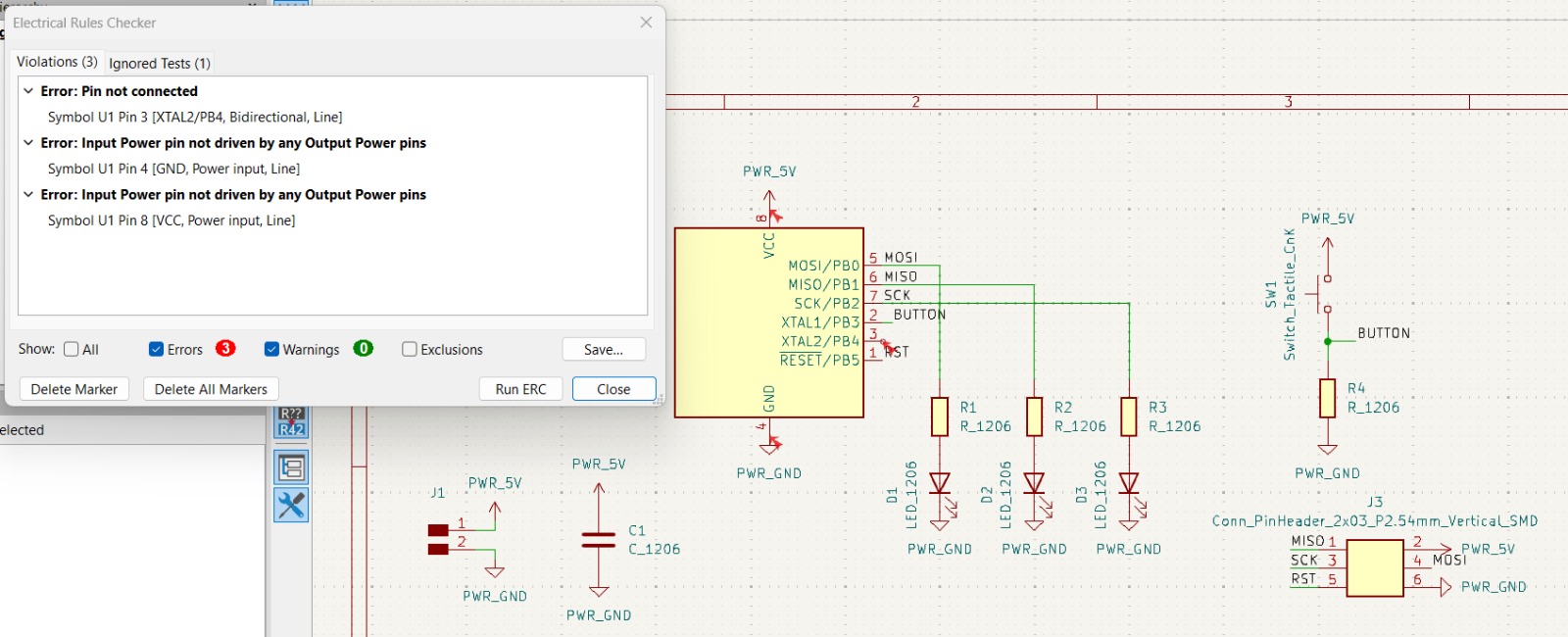
To ensure that everything is going well with our connections, we use the Inspect tool and Electrical Rules Checker. We observe that it only marks these three errors, which is fine.
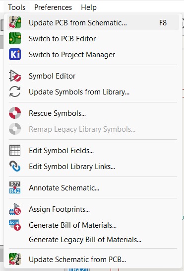
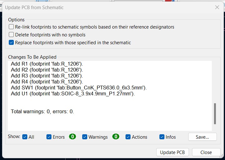
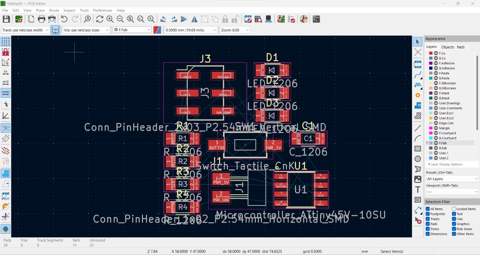
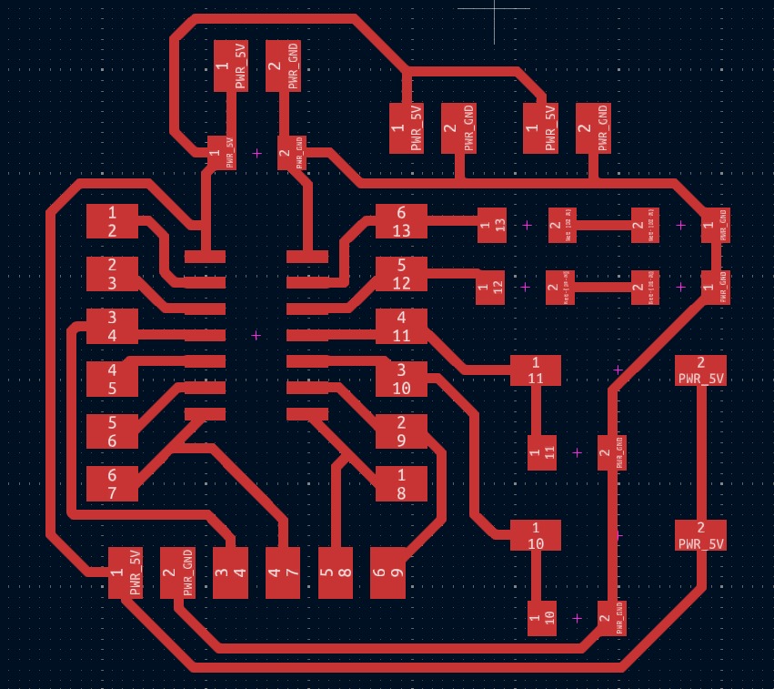
To update the PCB from the schematic, press the F8 key or click on "Update PCB from Schematic" in the toolbar. Then, click on "Update PCB and Close," and proceed to place the components on the PCB layout.
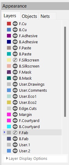
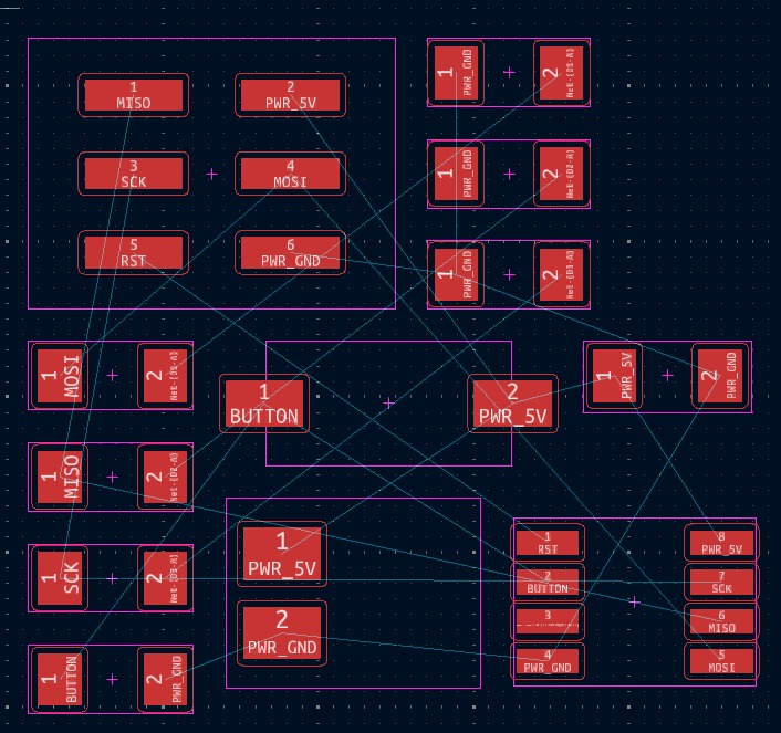
To organize the layout, we'll first remove the F.Fab view in the Appearance settings to only display the blue wires. Then, we'll arrange them to minimize crossings.
Much Better!
Before
After
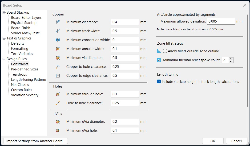
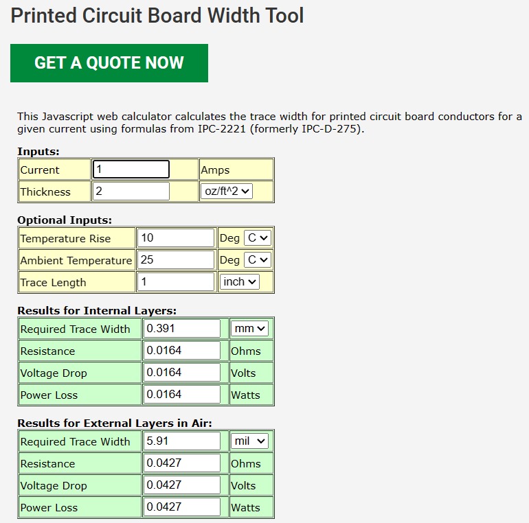
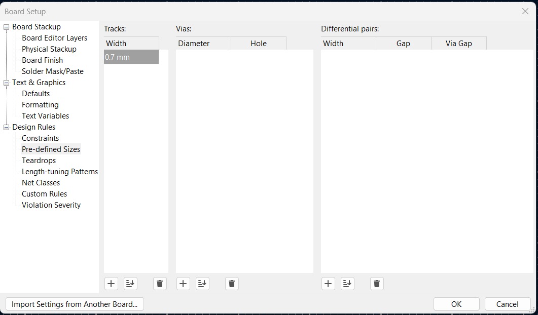
Next, we need to adjust the design rules. Follow these steps: File - Board Setup - Constraints. Change the Minimum clearance and minimum track width settings as needed. In this "trace width calculator" link, you will find the value for the traces based on the amperes required for your circuit design. In my case, I'll need a maximum of one ampere, so the calculator indicated that I only need a width of 0.39 mm, which rounded up would be 0.4 mm but I prefer that this be my clearance and I will add one milimeter 0.5 mm for my width.
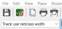
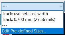
After that, under the saving and printing options, select the tracks and edit Pre-defined Sizes. Add 0.7 mm to the Width section for our tracks.
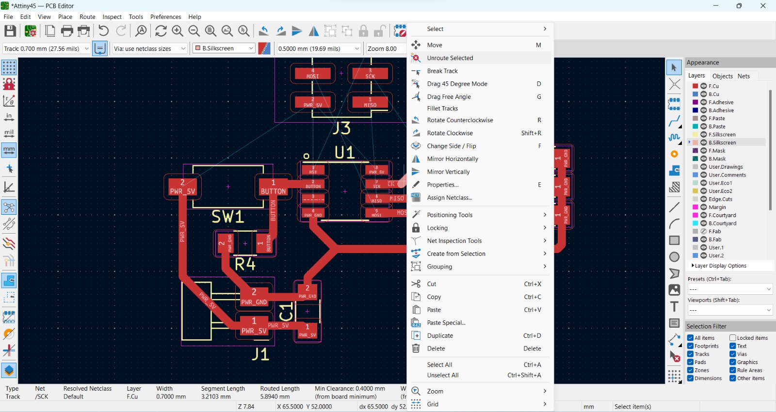
To connect the wires, use the X key, and to delete a whole trace, select it, right-click, and choose Unroute Selected.
It's fine to go back to the schematic to reorganize the connections if there are many crossed wires. Remember to update the PCB with F8 or click on "Update PCB from Schematic" in the Tools tab.
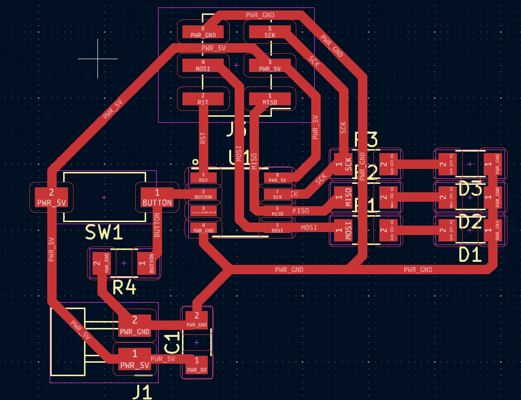
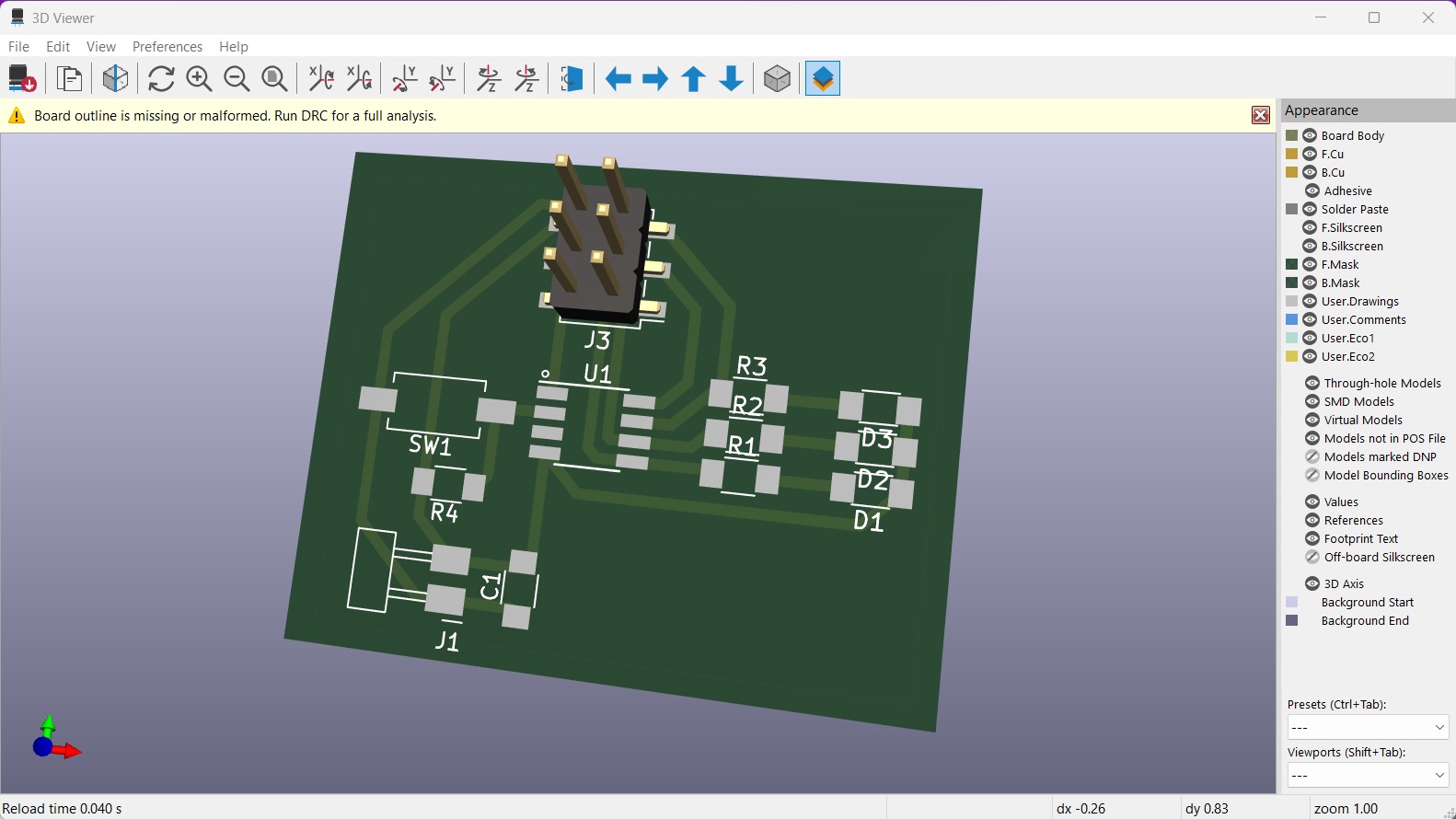
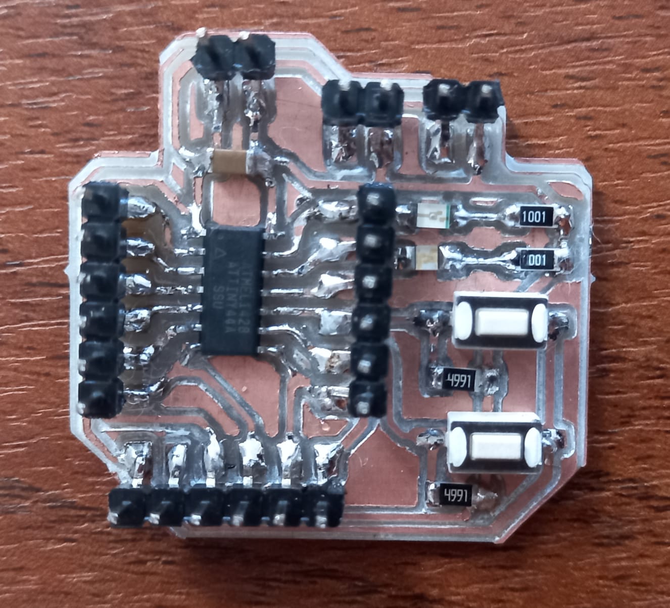
With these tools, I designed a circuit board for an Attiny44.
Before proceeding to export files, make sure to select "Edgecuts" layer, then draw a rectangle, circle, or polygon to outline the circuit.
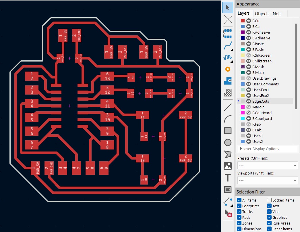
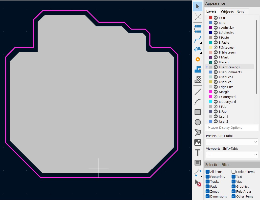
Afterward, select the "Margin" layer and draw the same shape, ensuring a one-millimeter space around it.
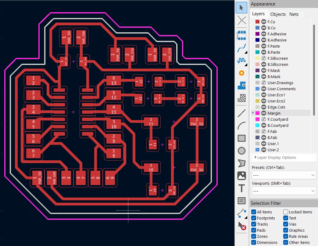
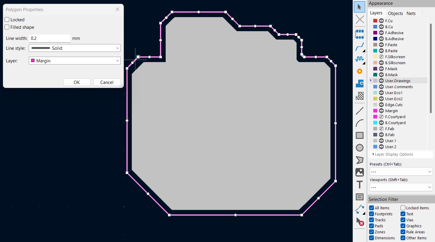
Finally, on the "User.drawings" layer, draw the shape of the Edgecuts with the filled shape option activated.
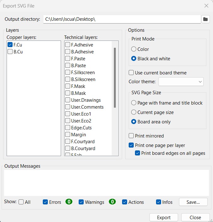
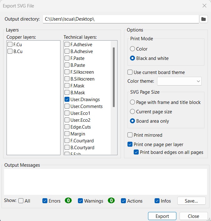
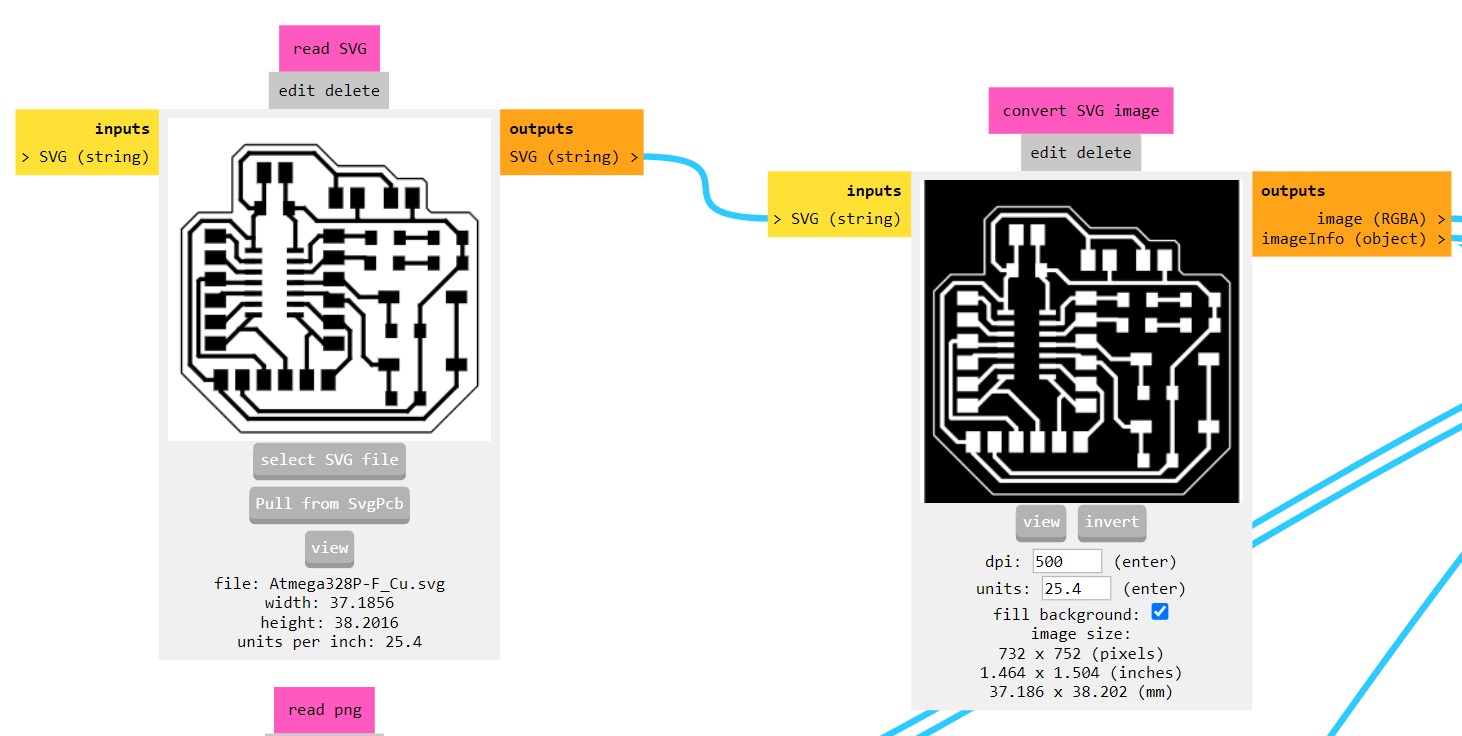
Time to export. Click on File - Export - SVG.
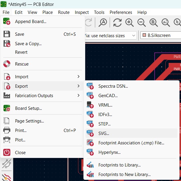
We are going to export two layers: first, F.Cu, which will contain the circuit traces, and second, User.Drawings, which will represent the circuit outline.
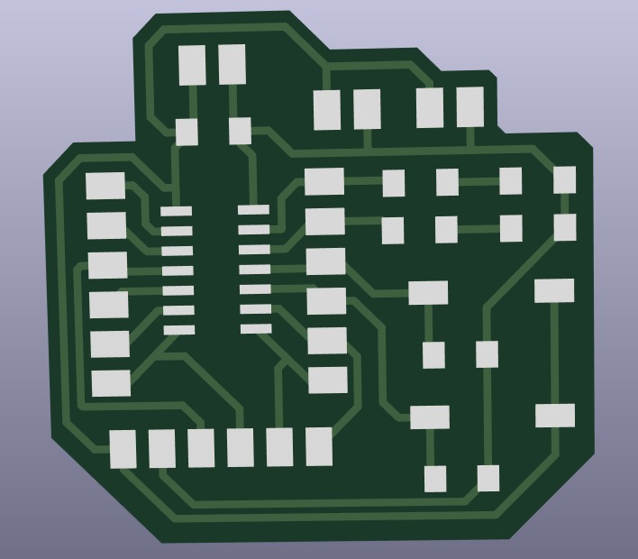
As well, you can see a 3D preview of the PCB by using the command Alt+3 or by selecting the option in the View tab.
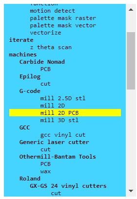
So, I used the knowledge learned in week 04 "Electronics Production" to generate the GCode and cut my copper plate.
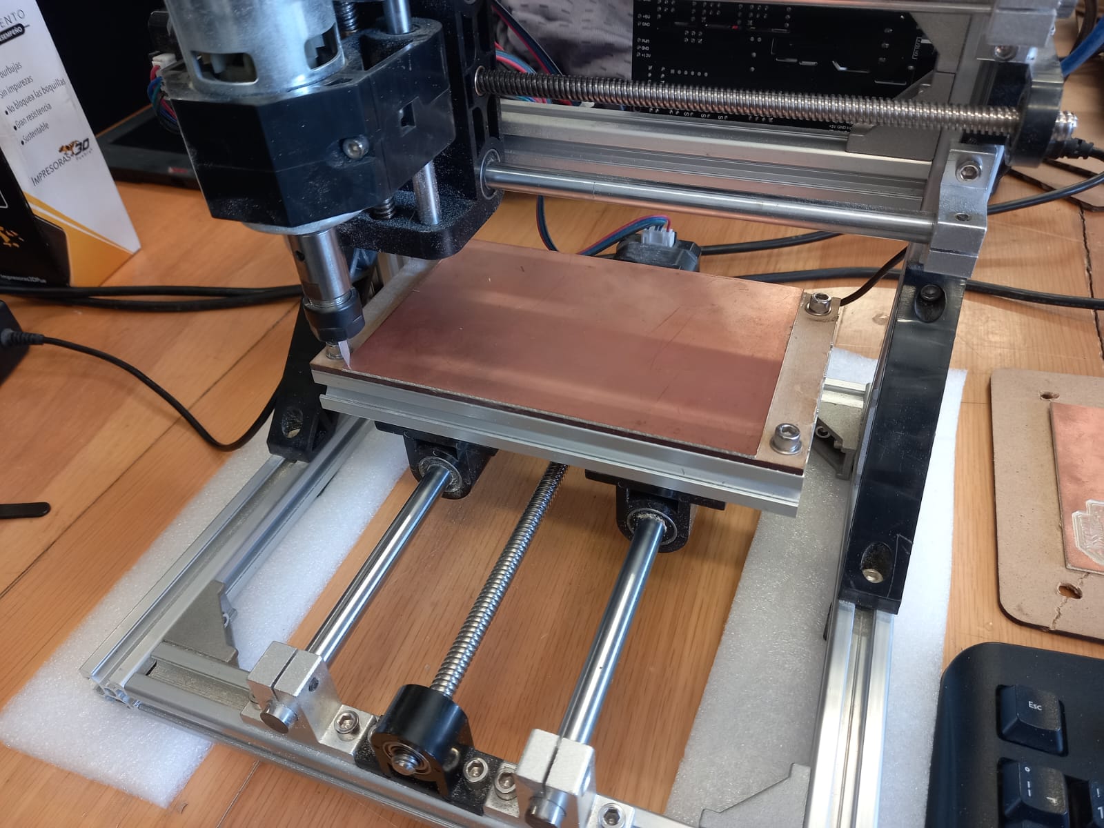
Here, I incorrectly set the Z-axis too low, causing the tool to penetrate too deeply into the copper plate. As a result, the cuts weren't made properly, leading to rough and uneven tracks.
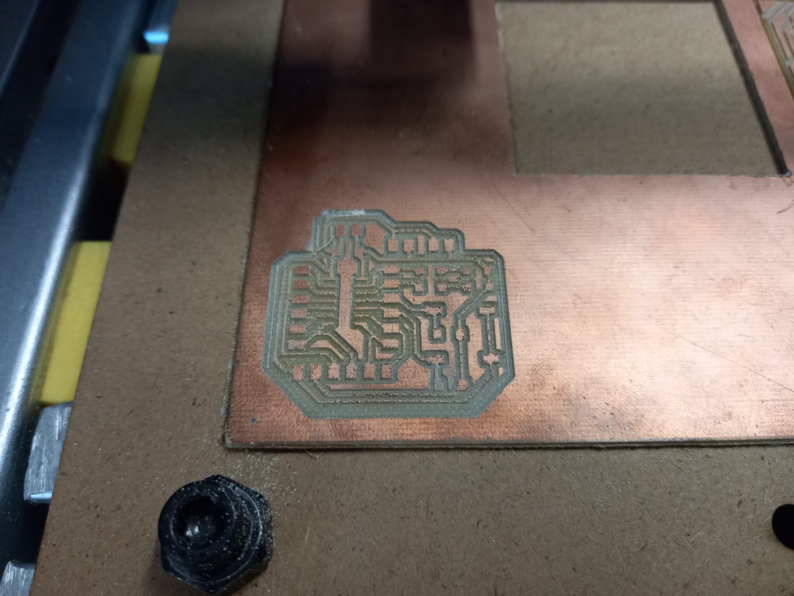
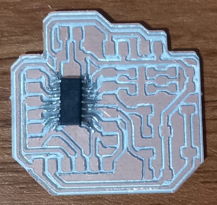
So, I adjusted it again, moving closer in the z-axis to the copper plate. Then, I loosened the grub screw gently until the tool made contact with the copper plate. After securing the tool, I spun it and descended just a micron to ensure it was cutting into the copper plate. The circuit board turned out better this way, so I started soldering. I tried my best jaja
Components list
- Attiny 44
- SMD capacitor 100 nF (or 0.1 µF)
- 2 SMD LEDs
- 2 SMD resistors (1001) for the LEDs (1000 ohms)
- 2 buttons
- 2 SMD resistors (4991) for the buttons (4990 ohms)
- 24 male pins
Testing
I used an Arduino Uno as ISP, if you want the step-by-step guide to program your Attiny, you can download the PDF on my website Práctica 3: Attiny85 Inputs in the Downloadable section (Click Here). I designed the circuit board with two buttons and two LEDs, with programming pins (RESET, MOSI, MISO, and SCK) and extra pins for sensors, other outputs, and PWR and GND on the circuit board. So, I programmed a code just to turn on the LEDs when pressing the buttons to check that works!
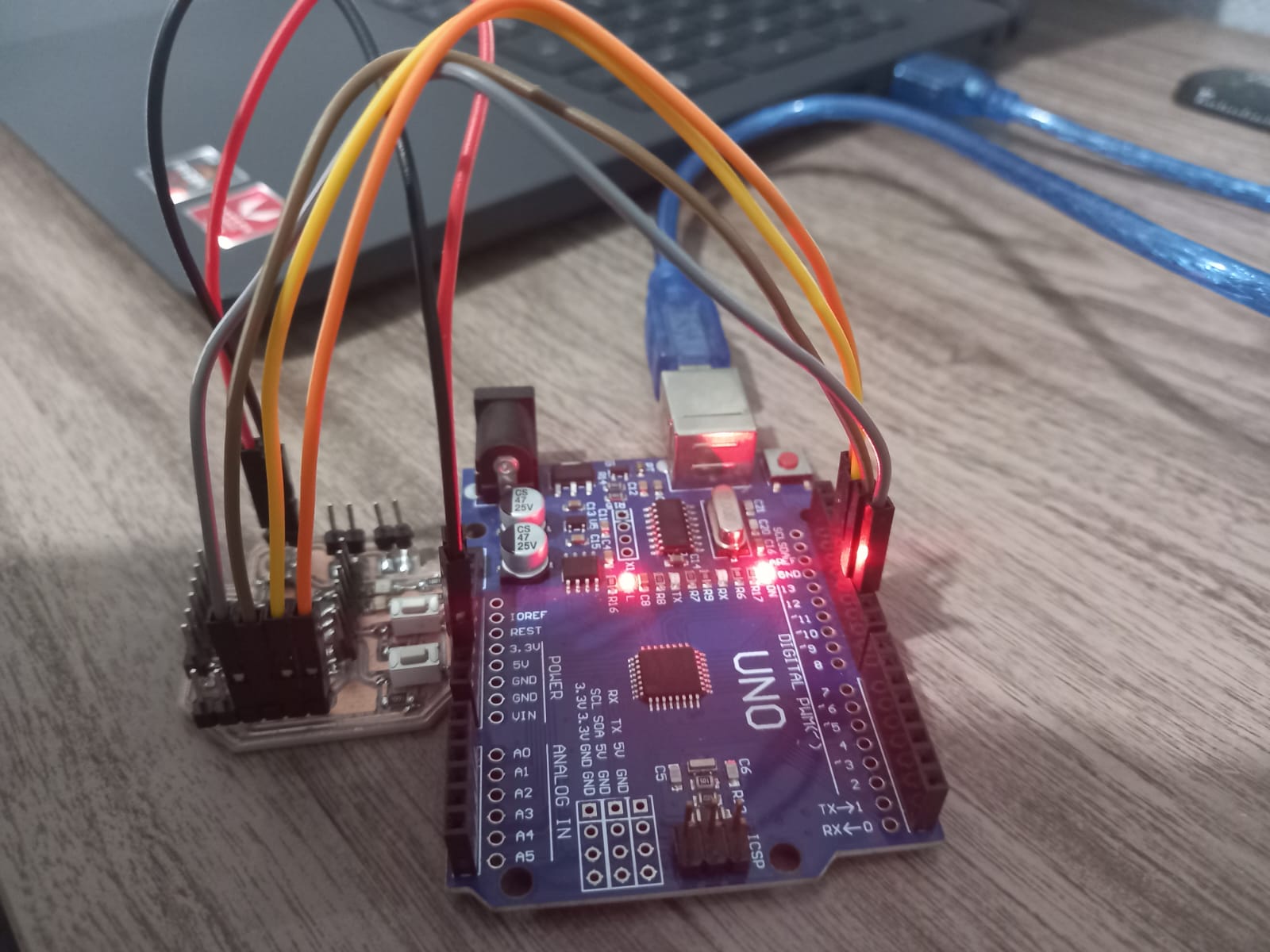
Buttons and LEDs