Electronics design
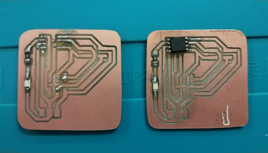
OH no!
Soldering Again...
To download Kicad click here!
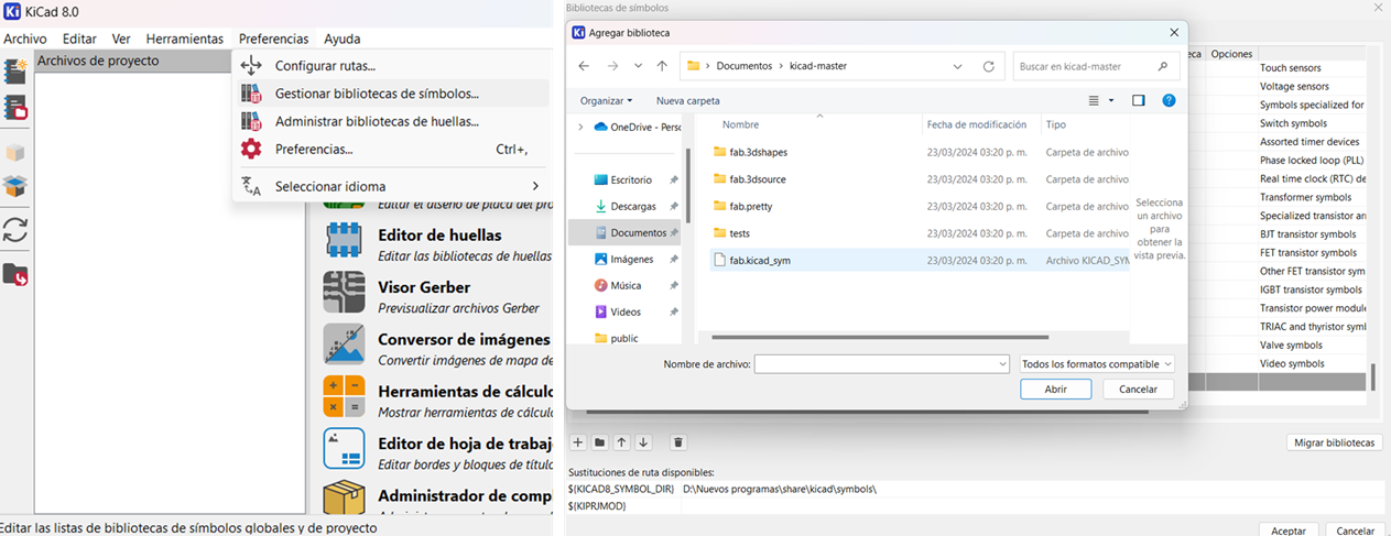
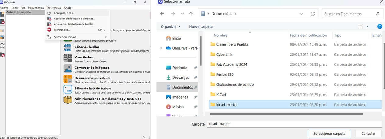
To start using Kicad you must manage the symbol and footprint libraries and configure paths
You can download the libraries Here
There are different design programs but. Kicad is much easier and free.
The first thing I did was click on "Manage preferences" and added the "Fab.kikad_sym" folder
NOTE: this is to download symbols
Now, to manage FOOTPRINTS we repeat the process but we are going to name the folder the same as the symbols folder but in lower case and we add the folder "fab.pretty"
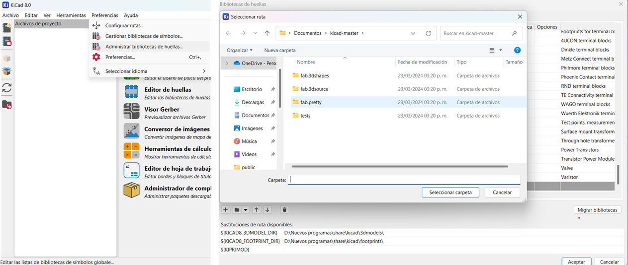
There are three files that we are loading because we need them, the schematic, the FOOTPRINT and the 3D model.
Now, for the 3D model we are going to configure the PATHS so, we open the paths configuration and add the entire folder and name it in capital letters.
We open a new project and name it whatever we want, in this case we will do a test with an electronic classic; an ATTINY 45V
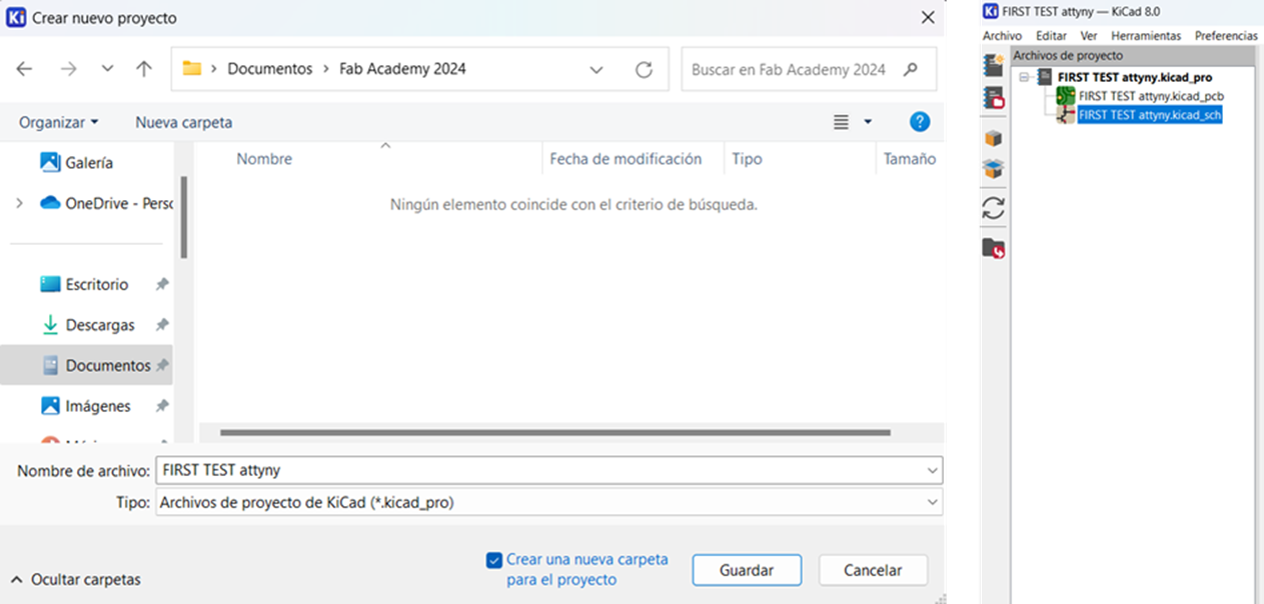
Let´s practice with an ATTINY
Click here to see the group assigment
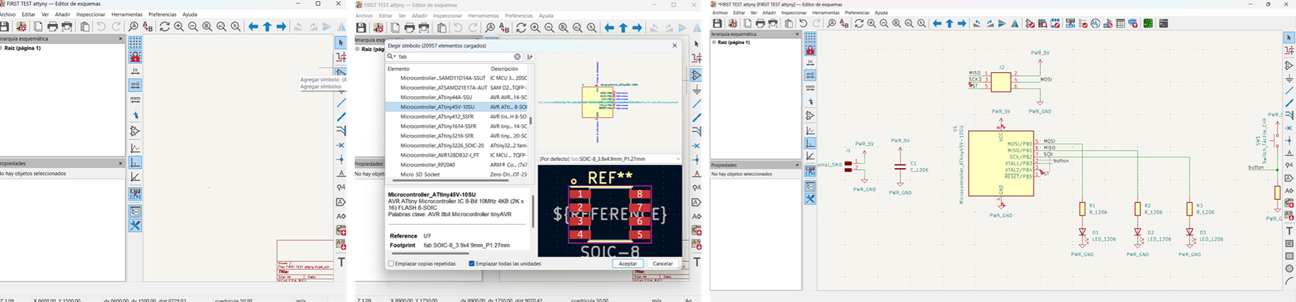
To begin, we open our project and view 2 windows: PCB and schematic. We will start with the schematic by double clicking on it.
NOTE: Think of the schematic as if it were a plan.
To add symbols we use the menu on the right. (The triangular symbol marked in blue)
For this example, we decided to include
- 3 LEDs and their respective resistors
- 1 button and its respective resistance
GROUND and VOLTAGE
How to connect it with PINS?Since many of the components need to be grounded, we are going to use the ground symbol that appears in the menu on the right to reference all of those components.
Invisible Bridges: To bridge the circuit without intertwining the connections, I can use references. In this case, we made the BUTTON reference with the option in the menu with the symbol "A"
CAPACITORS
The capacitors serve to filter voltage and ground, in this case, we include a capacitor between the pins and the microcontroller.We can select "Electrical rules checker" in the INSPECT menu and click "RUN" to see if there are any errors in our design. Now, it's not all errors, KICAD makes observations about some anomaly that is not necessarily an error, but rather some characteristics of the design.
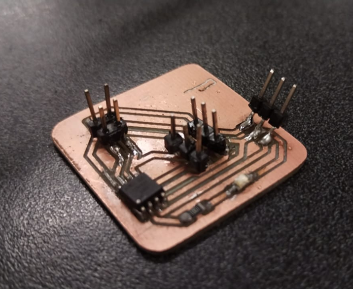
To program the microcontroller, we can use a USB connector but in this case we will use jumpered Programming PINS referenced in the correct order to program it.
The menu on the right shows us layers that indicate how we are going to machine the plate, for example.
F.C.u. to view the first layer of copper
F.Silkscreen to display or hide component labels
F.Fab For this exercise we also hide this layer so that the board is cleaner.
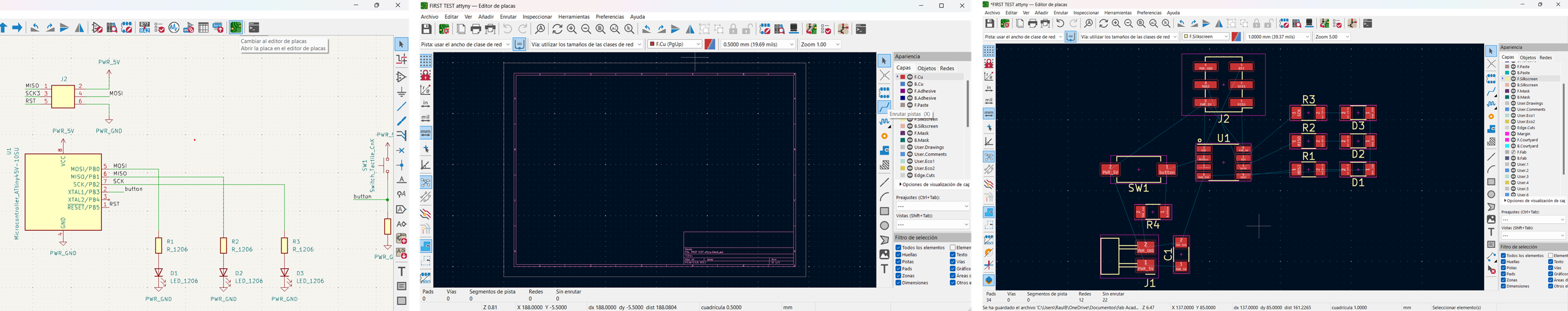
NOTE: We can also edit the track size in its own drop-down menu.
Now, to create the cut line, we select "Edge CUTS" in the layers menu and with the drawing tool we create a rectangle around the design.
We use the "Margin" layer to establish a diameter of 1 mm distance so that it cuts on the outside and with the "User Drawings" layer we create a rectangle that covers the entire design, that way, when we export we can select only the margin.
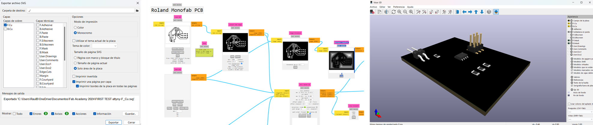
NOTE: Kicad allows you to view the 3D model
This is my first design
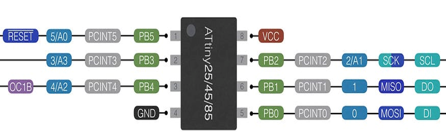
I decided to use an Attiny 45 microcontroller because it is a classic in the world of programming and its possibilities are ideal for the project I have in mind.In the PINOUT diagram we can see that the microcontroller has pins (SCK, MISO, MOSI SCL and SDA), which will be very convenient for future exercises.
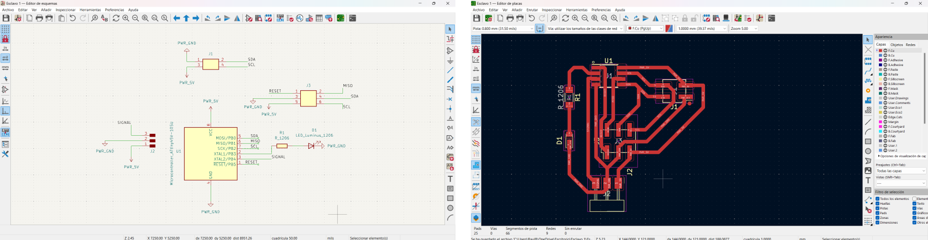
In the schematic it can be seen that:
Add the 3 output pins that a servo motor uses (Ground, Voltage and Signal)
An LED with its respective 1K resistor
The output PINOUT to program the Attiny (Reset,GND, Voltage, MISO, SCK and MOSI)
Also add the output pins (SDA and SCL with GND and voltage) for an I2C communication (My Instructor's Suggestion)
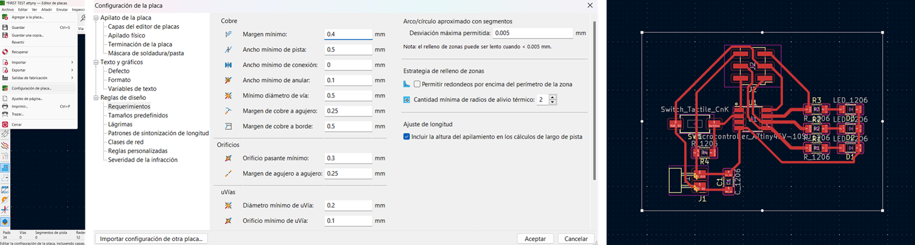
ERC & DRC
Electrical rules checker & Design rules Checker
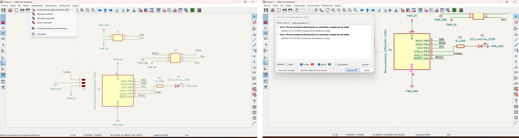
KiCad has an option to verify that your board layout is correct. By selecting the "electrical rules checker" option in the "Inspect" menu you can open a window that indicates possible design errors.If you click on the "Run ERC" option, the errors appear. In my case, 2 errors appear that I can ignore, since, in my design, Voltage and Ground are only connected to a label that will be used to make the connections in the "PCB Editor"
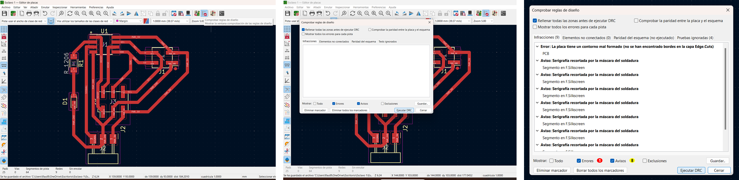
In the "PCB Editor" you can perform a general check like in the Schematic by selecting the "electrical rules checker" option in "Inspect" menu.
If you click on the "Run DRC" option, the errors appear. In my case, KiCad automatically suggests that I use the "edge cuts" layer for the edges of the PCB, but I decided to use the "Margin" layer to create the outline. I also get the error "Silkscreen clipped by solder mask but, I can ignore them because, my board doesn't have any paint marks on it, so it's fine if I cut it like this.
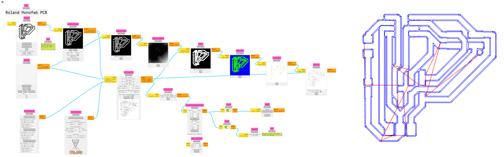
Settings in Mods
The same process from Week 4
BIG MISTAKE!
While soldering the Attiny onto the board, two tracks got soldered together and while trying to fix it, I completely detached one track, so I had to cut a new one, from a piece of board that a colleague gave me.