8. Electronic Design
Week asignments
1. Group assignment: use the test equipment in your lab to observe the operation of a microcontroller circuit board. Send a PCB out to a board house.
2.Individual assignment: use an EDA tool to design a development board to interact and communicate with an embedded microcontroller.
Group asignment
Check out the Puebla FabLab repository: https://fabacademy.org/2024/labs/puebla/week8/
Individual asignment: making the remote control PCB
This week we learned how to use KiCad 8.0. This is an EDA tool, free of charge, and quite complete since libraries for FAB components exist. We need to start by defining how to use the tool
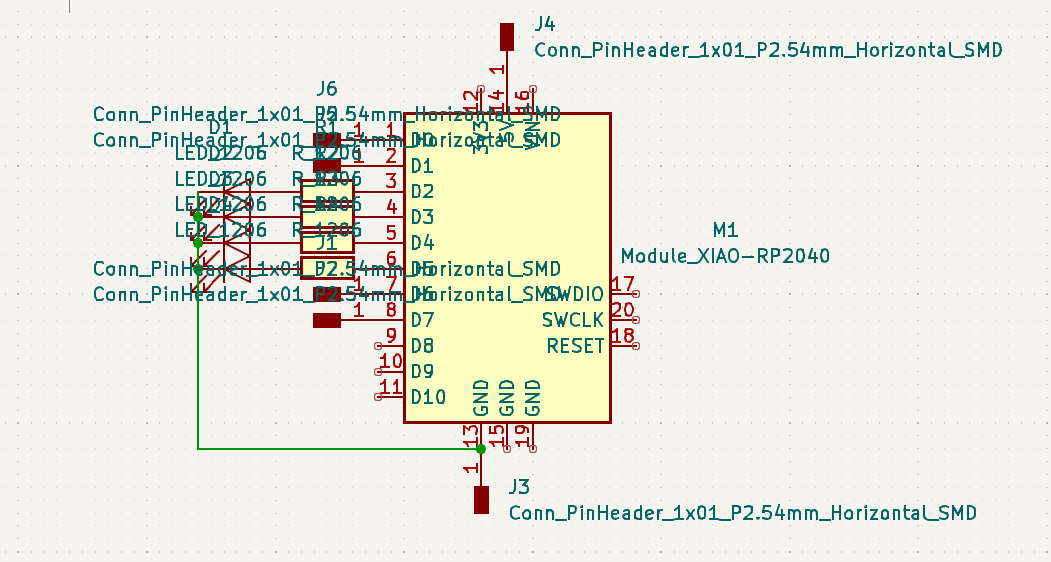
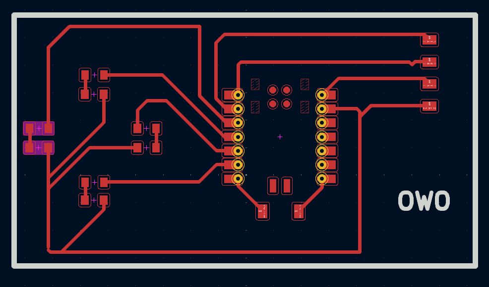
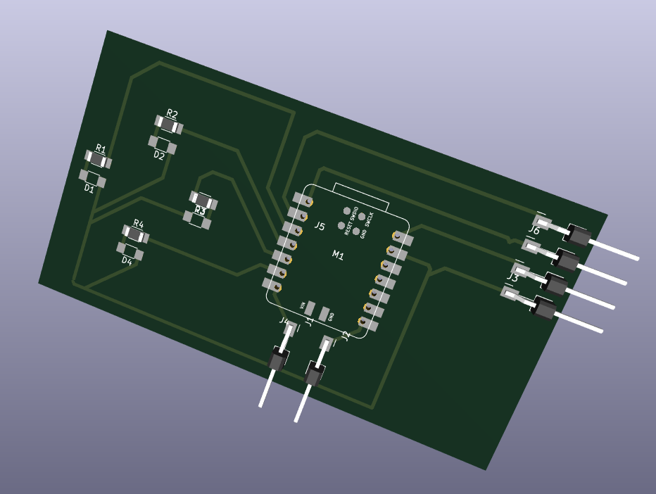
The design of my board, focused on my final projects remote control, will interact with an input: joystick and an output: LED array like control arrows in a keyboard.
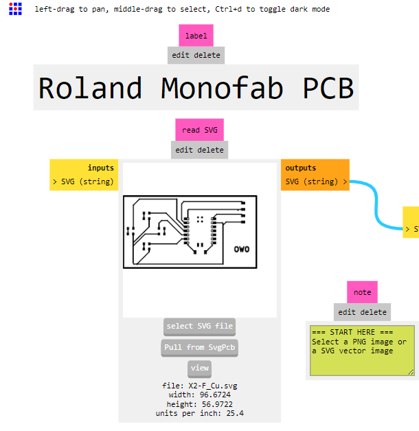
SCHEMATIC
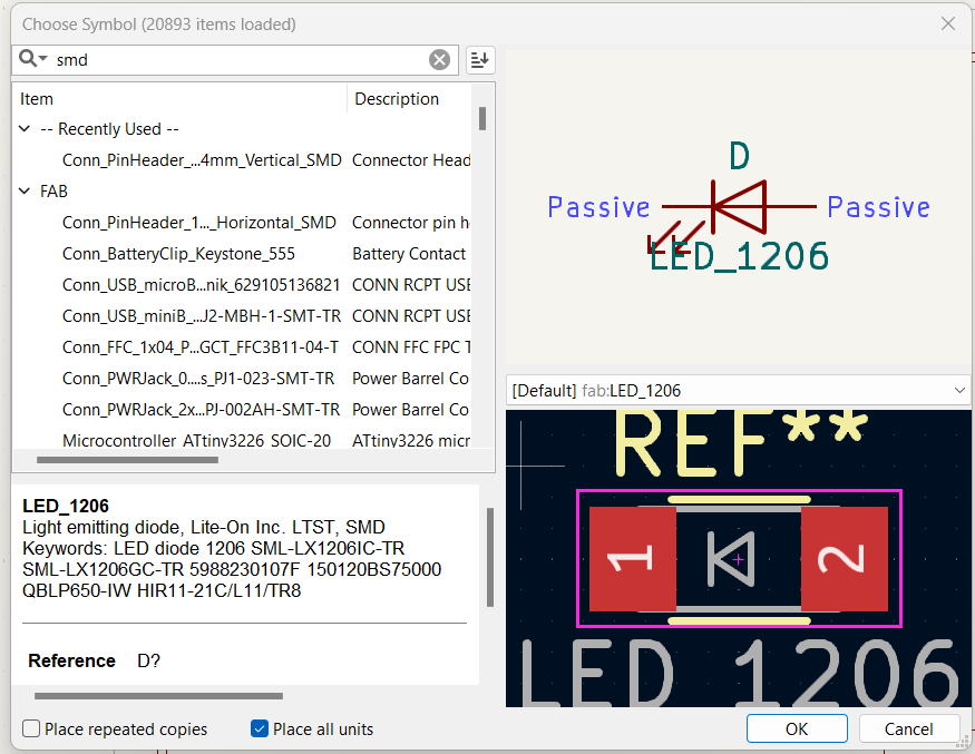
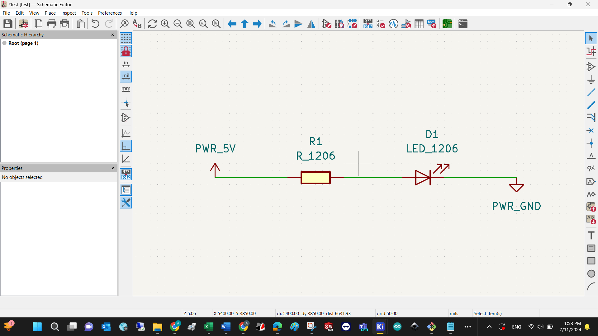
Start by dragging and dropping in the canvas all the components you will need. Make sure to connect everything in a circuit way, circuit means closed loop. If your design turns too complex, you can used tags so you don’t get lost. I’ll start with a simple example for an LED and a Resistor.
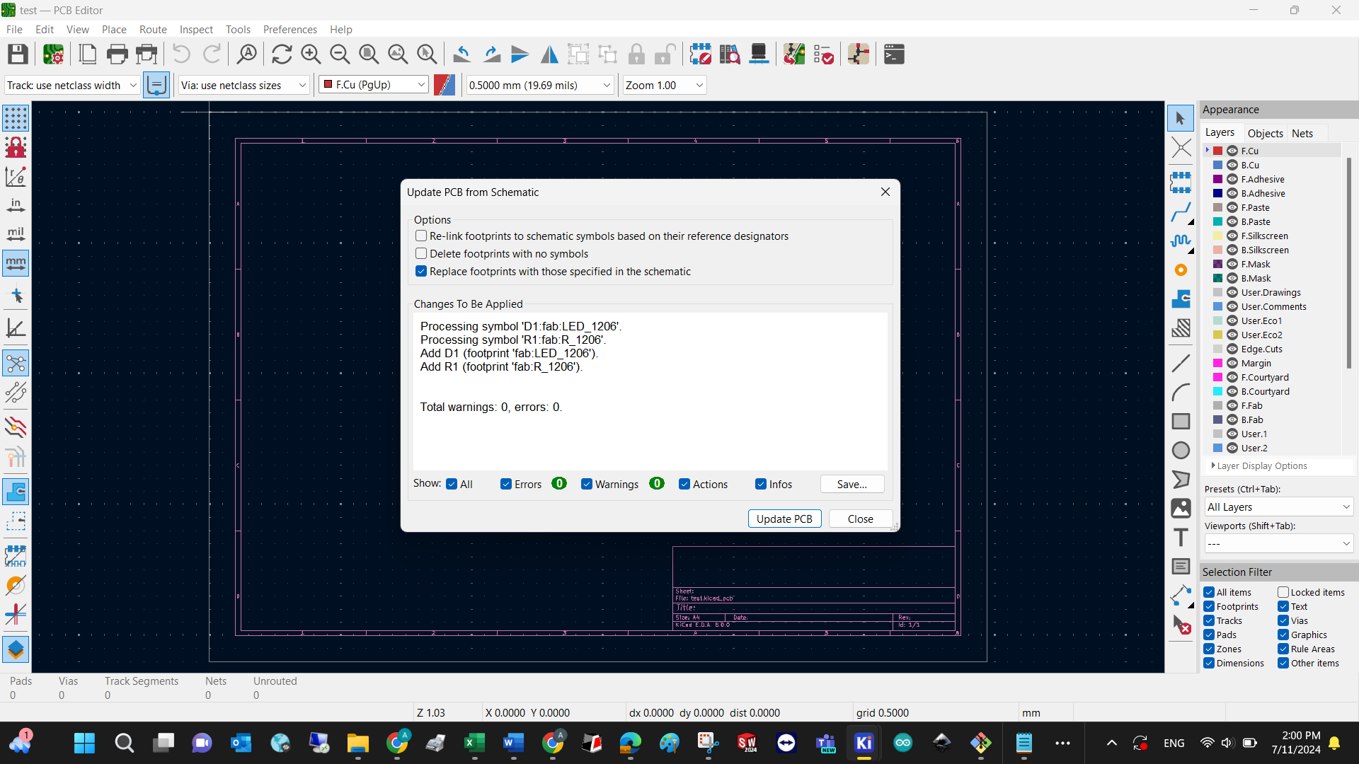
PCB DESIGN
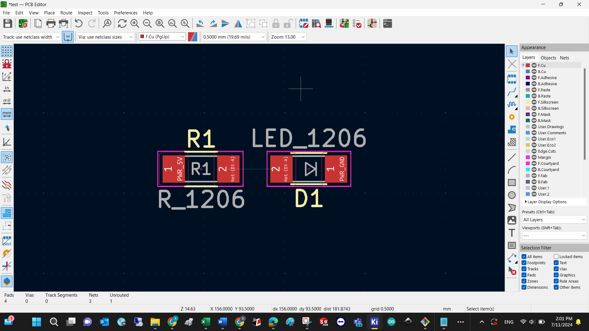
If you open the PCB Editor and is blank, that means that the files were not updated. After you click on the update PCB button, you can start rearranging the component layout (element distribution across your working area)
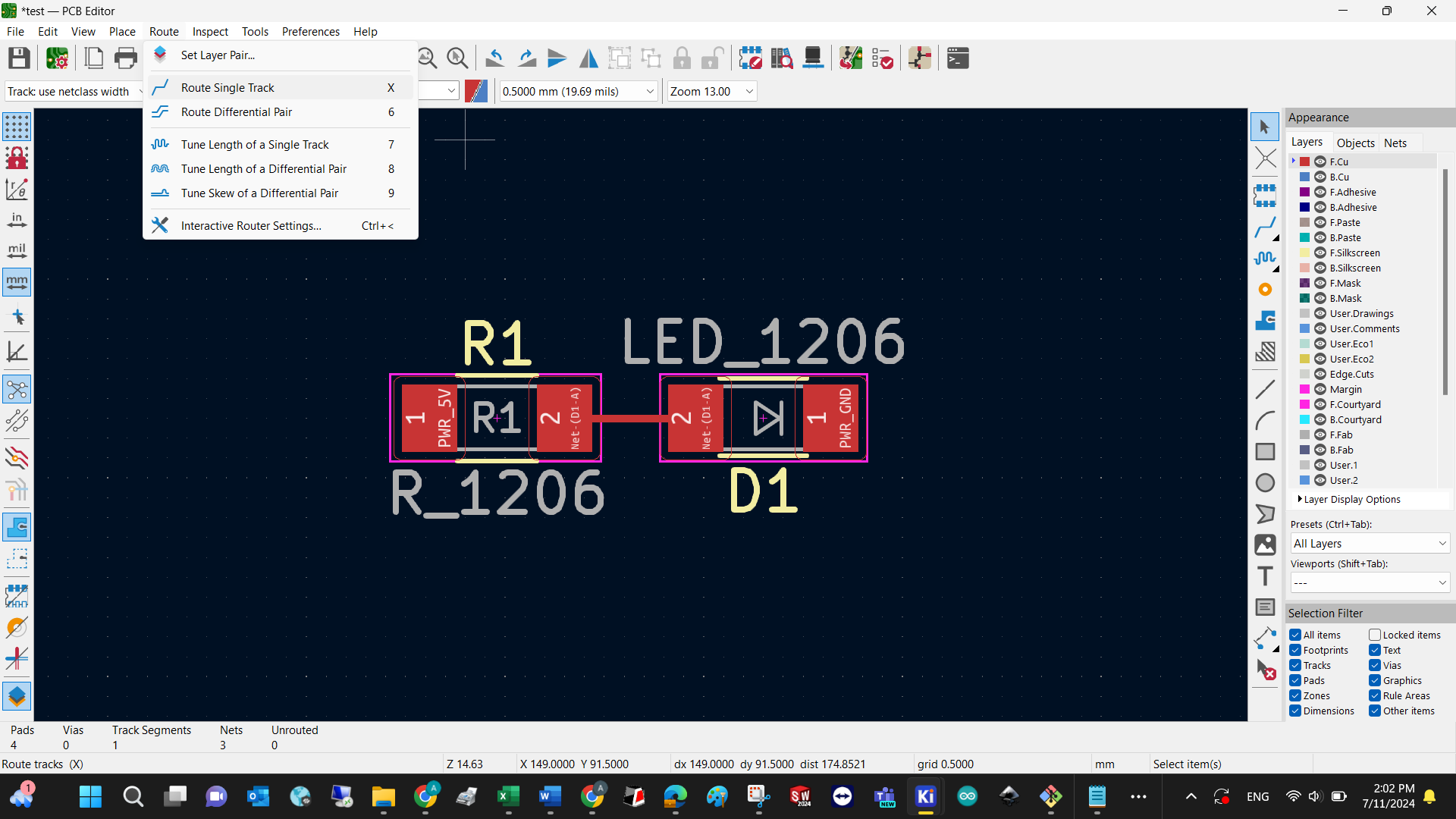
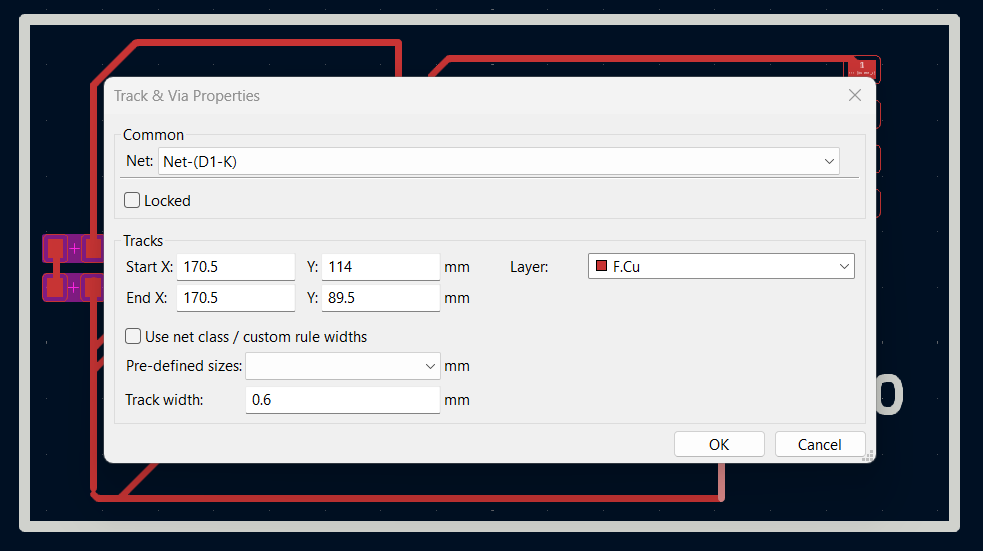
Once you are happy, start connecting the terminals (routing traces) with the respective component. The mental challenge here is to avoid crossing paths and try to merge all the grounds from your design
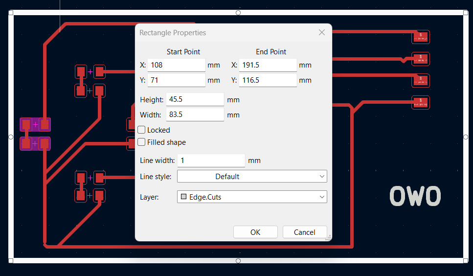
Create a rectangle or a defined shape to provide your design with an outer form. Rectangular designs are boring but functional. I would like to test crazier shapes after that.
We need to think in terms of layers. For beginner purposes, lets consider 2 types: Fcu for the traces or copper lines that will connect components, and EdgeCuts for the outer shape of our design. Make sure you have the following parameter by clicking twice on each type of line.
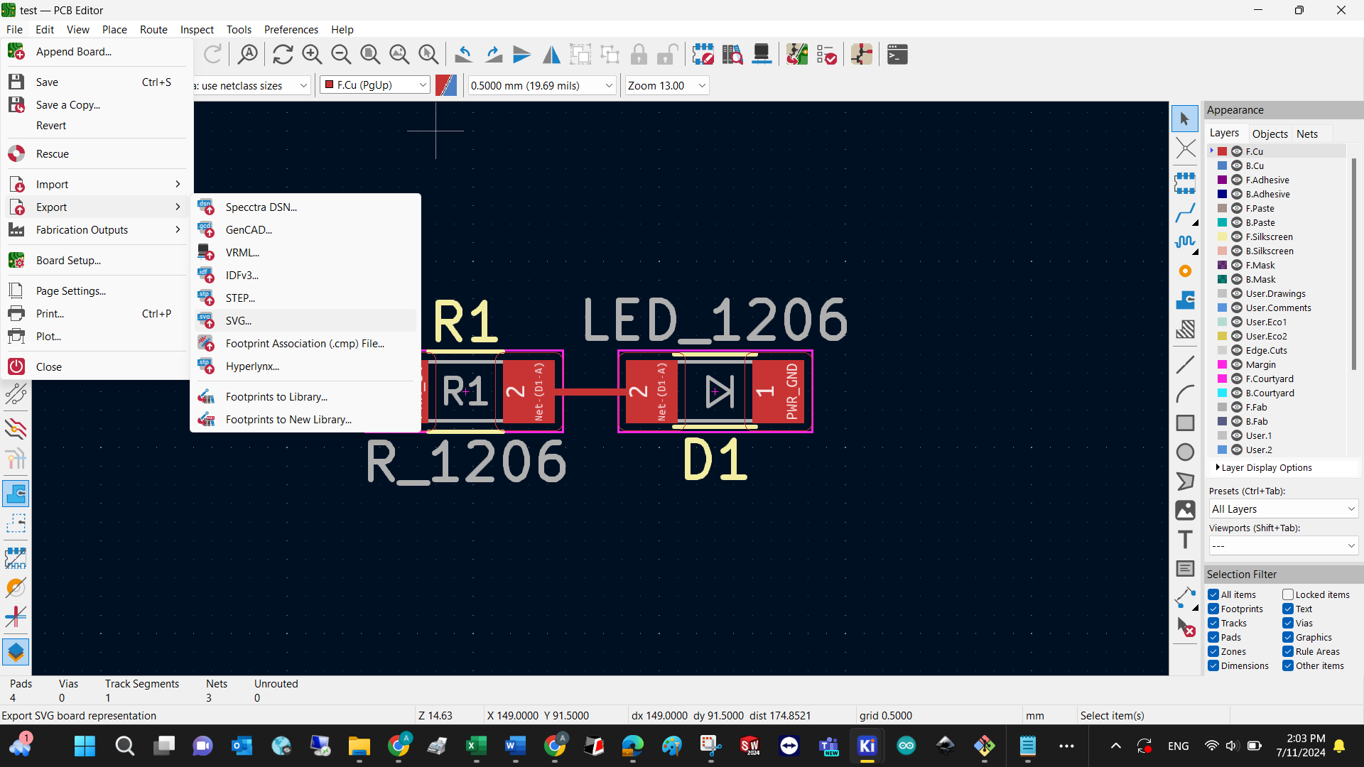
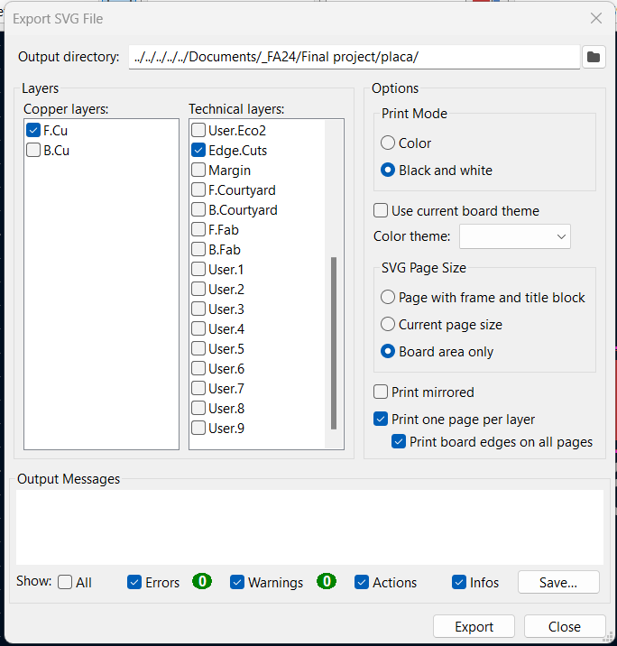
Export both the PCB traces and the Outline of your PCB as .svg to use them in the next part of the process.
If you want to know how your board would look in 3D, you can render the results by pressing alt+3 or clicking the 3D view
MODS
What (the hell) is this? As the gitlab repository where it is contained says, mods was originally written by Neil Gershenfeld for rapid-prototyping workflows in CBA research and classes, and for use in the fab lab network and its classes. https://modsproject.org/
PROCESS FOR TRACES
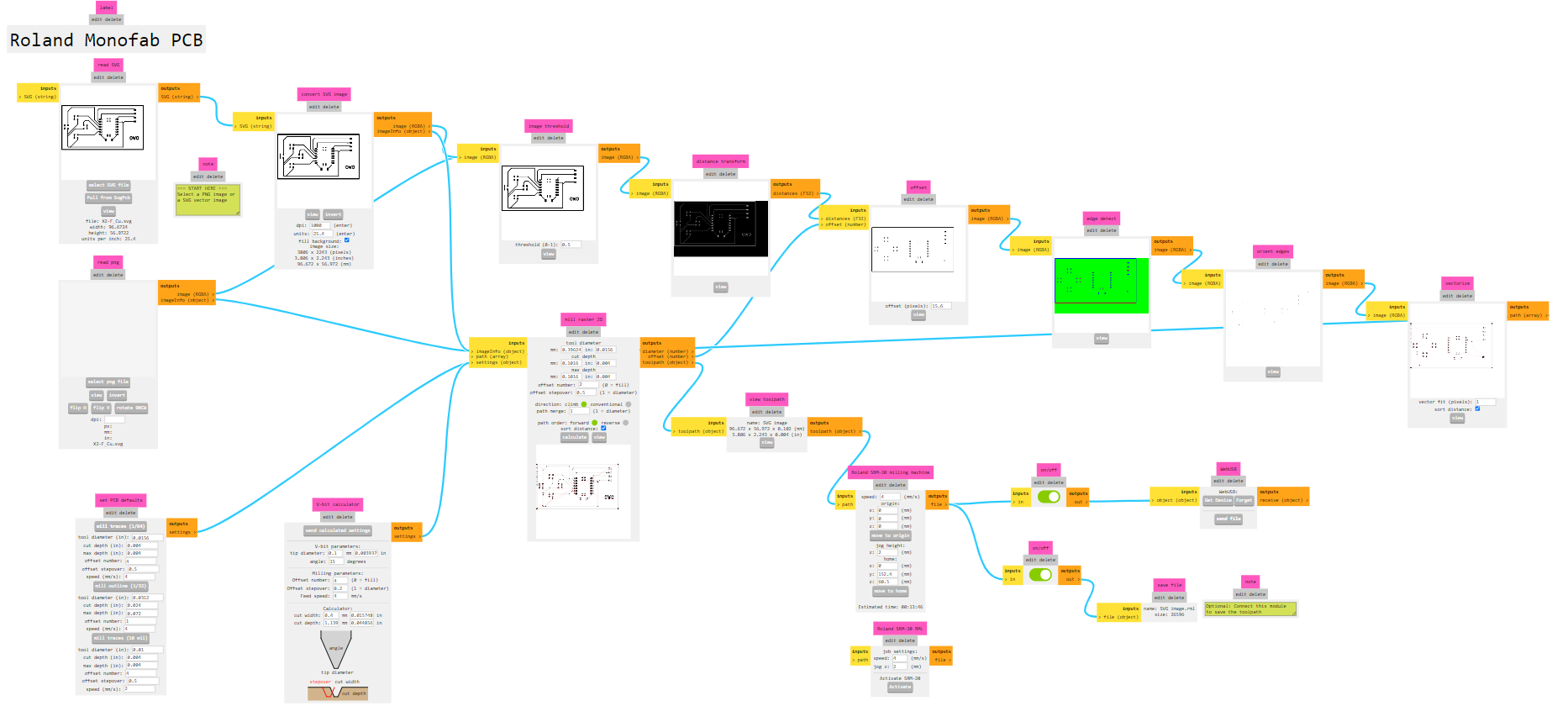
Open mods/programs/open program/Roland/SRM-20 mill/mill 2D PCB. A huge network of operations will appear, but you only need to modify a few (you can tell them for the text box color: pink!):
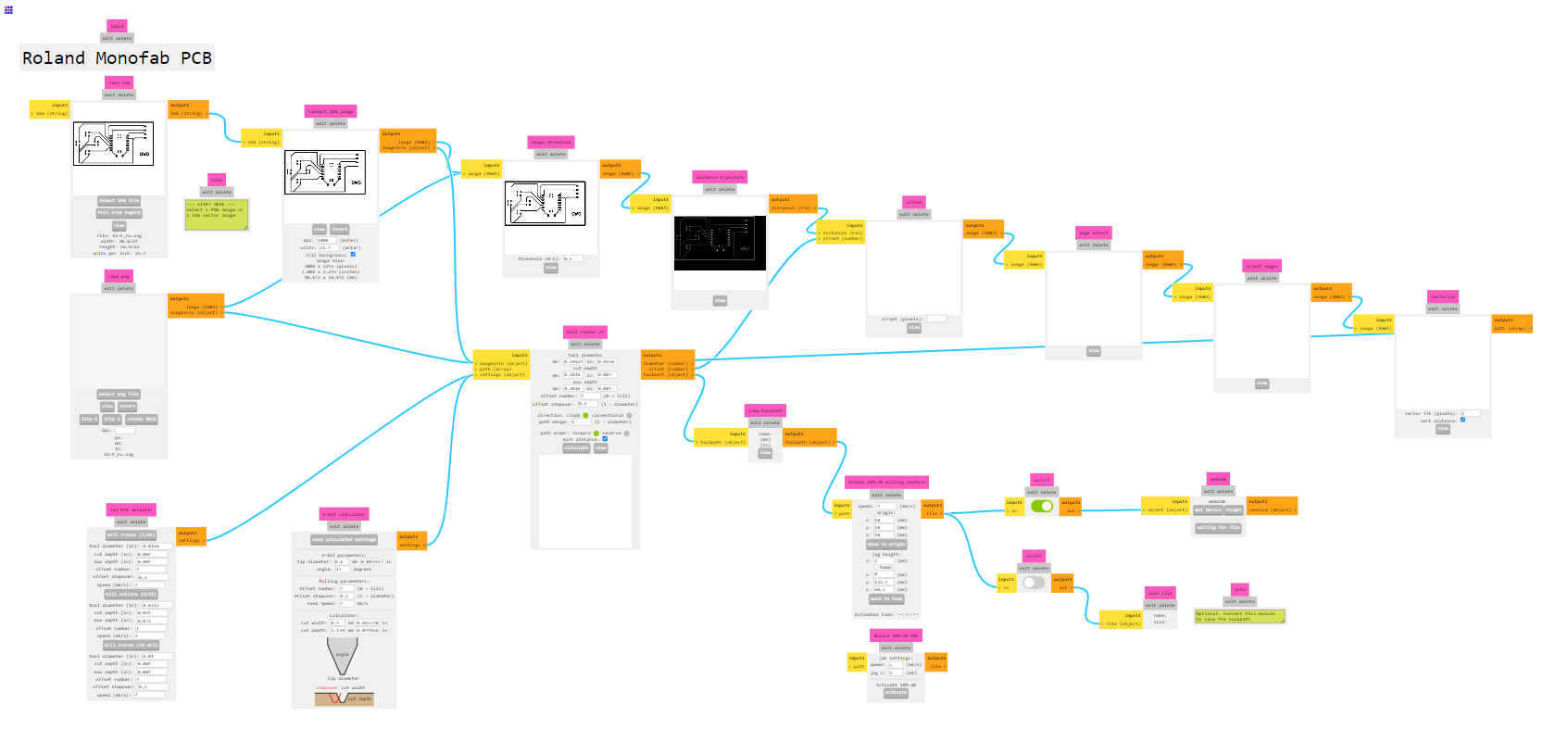
- Read svg: place the svg file from the traces.
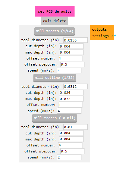
- Set pcb defaults: select mill traces (1/64)
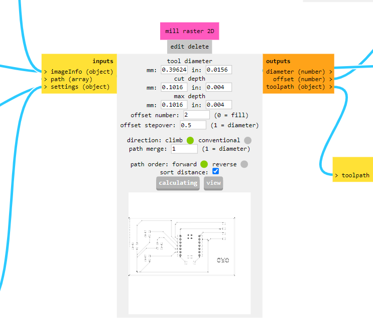
- Mill raster 2D: change offset number value to 2 and click calculate
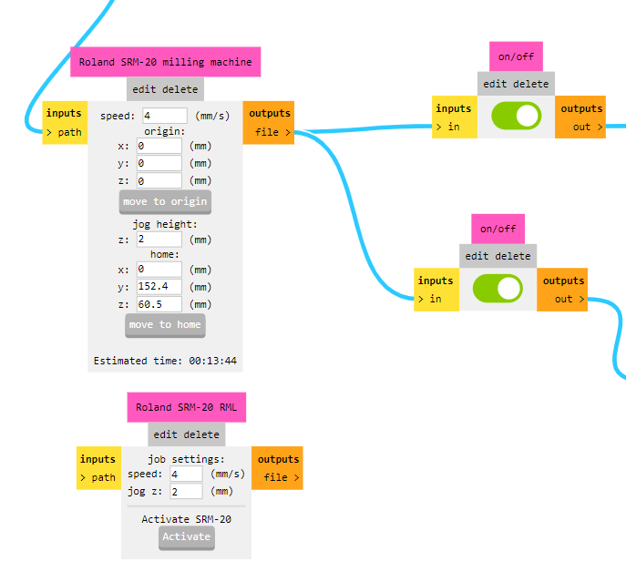
- Roland SRM-20 milling machine: set the origins x,y,z to 0. Make sure the second switch is on
- Mill raster 2D: click calculate and a .RML file will be downloaded
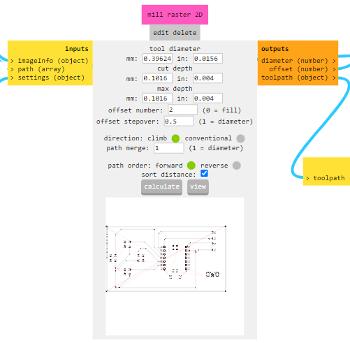
Can you notice the differences between the first version of the image below and the second version?
PROCESS FOR CUTS
- Read png: upload cut file and invert it.
- Set PCB defaults: select mill outline (1/32)
- Mill Raster 2D: Change the tool diameter to 0.8, enable the second switch, set to x,y,z to 0, . Click calculate, , and the .RML file for the cut will be downloaded. Sometimes it’s open in another window
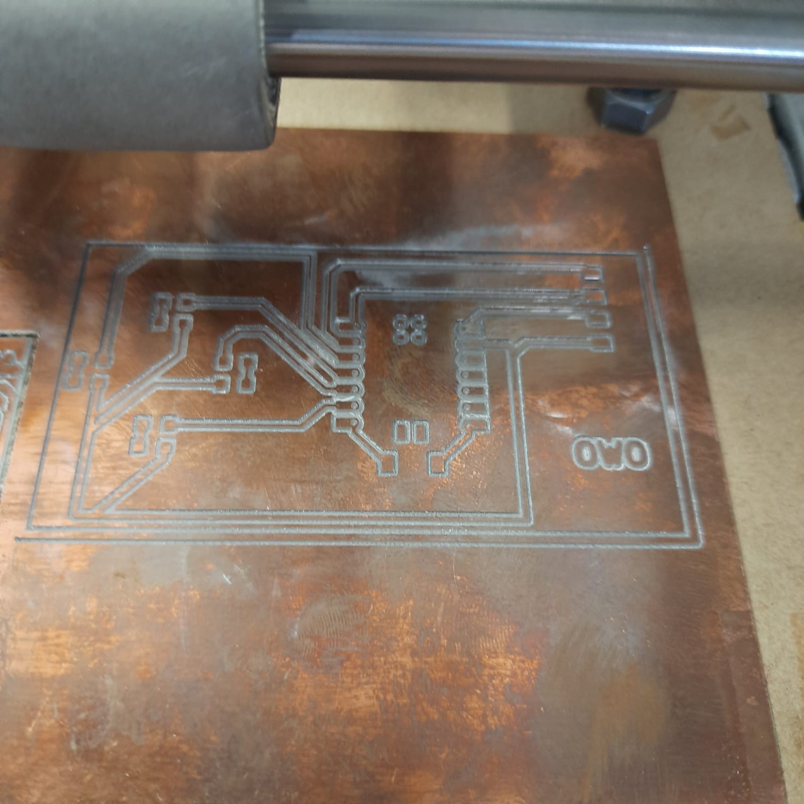
MANUFACTURE
Follow the steps that were explained in week 4. A summary of them: Schedule time for the Roland. Get your copper plate mounted in the specific mdf plates, stick them together with double-sided tape. Mount them inside the Roland. Mount the traces cutter. Connect the V Panel to control the Roland, set the x,y,z origins. Import the traces file and start milling. When the milling process is done, clean the fiberglass with a vacuum cleaner. Change the tool to the outside cutter. Only reset the Z axis. Start milling. Clean and remove material when the process is done.
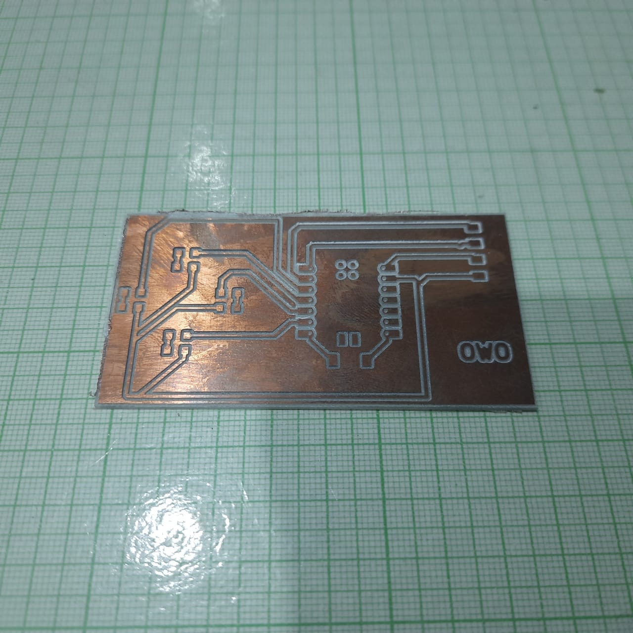
Thanks to Gaby Tamanis for lending a hand in the creation of the prototype
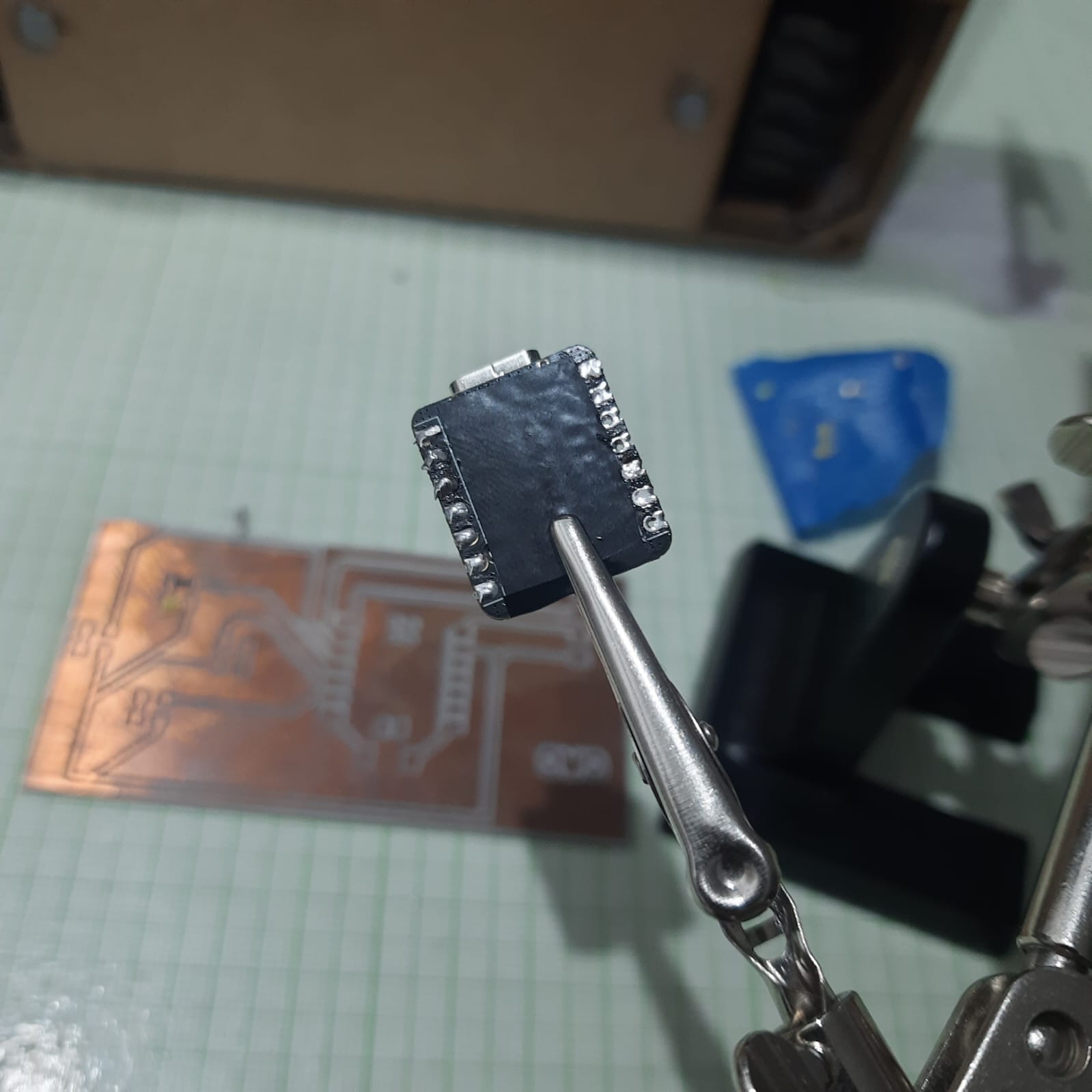
SOLDERING AND TESTING
Try to do it in a clean workbench with clean air removing dangerous fumes. If you are working with a Xiao from Seeed, try masking the back of the PCB. Let the heat dissipate so the soldering is uniformly applied.
For testing purposes, there are two ways: full system testing (hoping everything works for the first time: just writing a program to enable each output at the same time) and individual testing (if something fails, you have to narrow it down to the most common component that might be the issue) IMPORTANT: If you have trust issues like the author if this document, you can test each component even before mounting them. I was on a confident mood (lie, I was just out of time like the last 6 months) and executed the full system testing. Everything worked ;)