8. Electronic design
Electronics Design
Electronic design is the process of creating, testing, and producing electronic systems and circuits. The goals of electronic design can range from creating a functional prototype to the development of marketable and production-efficient electronic products.
It involves several stages, including:
- Requirement Definition: Establishing the objectives and needs of the project.
- Component Selection: Choosing the appropriate components based on technical specifications and compatibility.
- Schematic Design: Creating a diagram that shows the connections between components.
- PCB Design: Designing the printed circuit board, planning the location of components and the routes of the connections.
- Simulation and Prototyping: Simulating the circuit and building prototypes for testing.
- Testing and Validation: Verifying that the prototype meets the established requirements and standards.
- Production: Manufacturing the product or system in mass after validating the design.
For this practice, we used some electronic tools and components. For more information, please visit the GROUP PAGE .
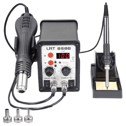
soldering station
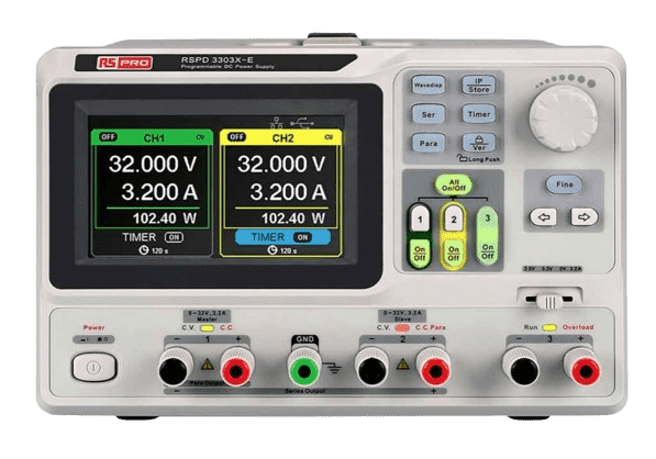
power supply
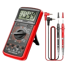
Multimeter
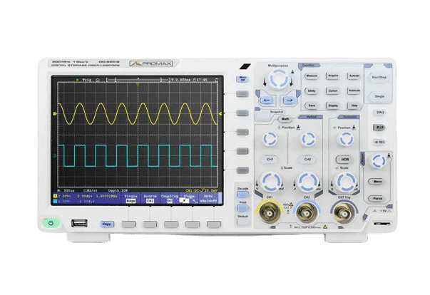
oscilloscope
boards
EDA tools
EDA, or Electronic Design Automation, refers to a set of software tools used to design electronic systems such as integrated circuits and printed circuit boards. EDA tools automate parts of the design and testing process of electronic components, allowing engineers to design more complex products in less time than would be possible manually.
program

kicad


 |
These tools are the labels, with which we can connect pins without needing to see the wires. |
 |
Wire, with this tool we can make connections between pins. |
 |
Add symbols, this allows us to add all the components we will be using. |
 |
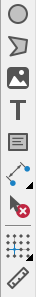
Basic shapes tools. |
 |
Open the PCB, this will open the PCB file linked to this project. |


 |
Update the changes from our schematic in our PCB. |
 |
Wire, makes the physical connections between the pins. |
 |
Basic shapes tools. |
 |
Allows us to add images to our file, to use them as a reference. |
 |
Allows us to set a real measurement |
Design
Before starting the PCB design, I first considered what I would use the board for. Since I didn't have a specific use in mind and wanted it to function for future tests, I decided to make a board that would allow me to use all the pins of my microcontroller, so I could conduct various tests before designing a special board for my final project. Download the library


for this Proyect
Requirement
Design and create a board with all the capabilities of an Arduino Nano, with additional outputs for some external components.This board will be useful for testing the different components that I will use in the coming weeks and for some tests for the final project.
Component Selection
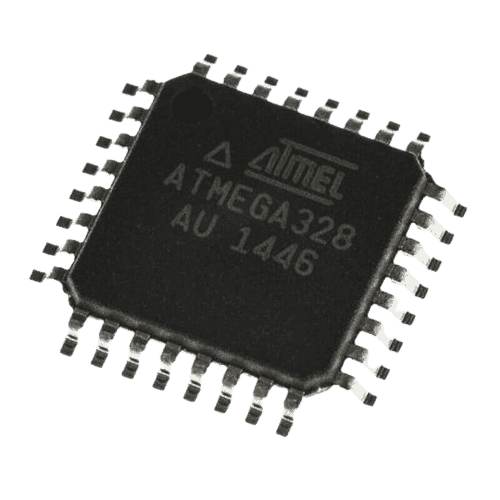
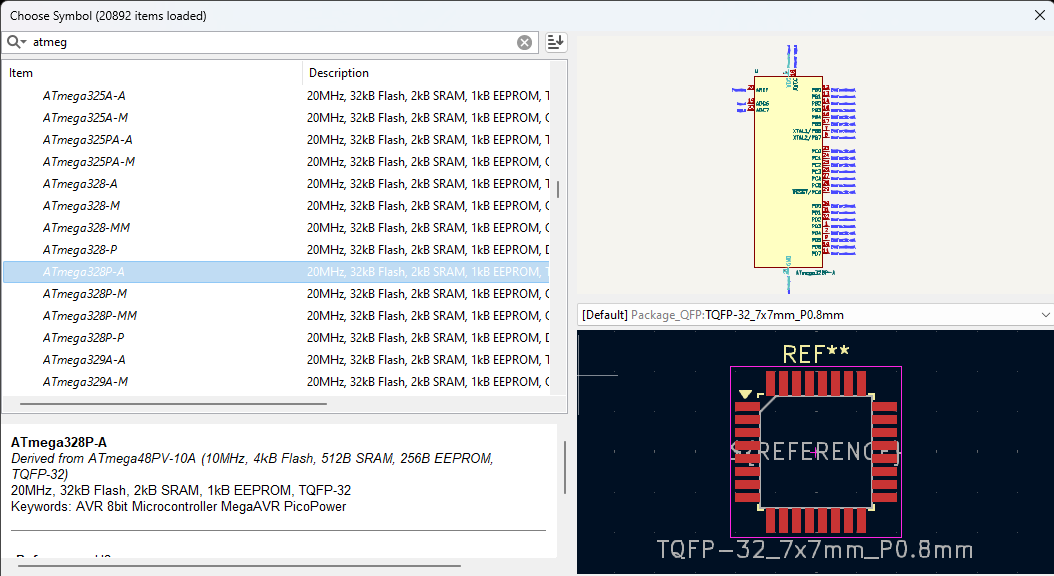
- Atmega328
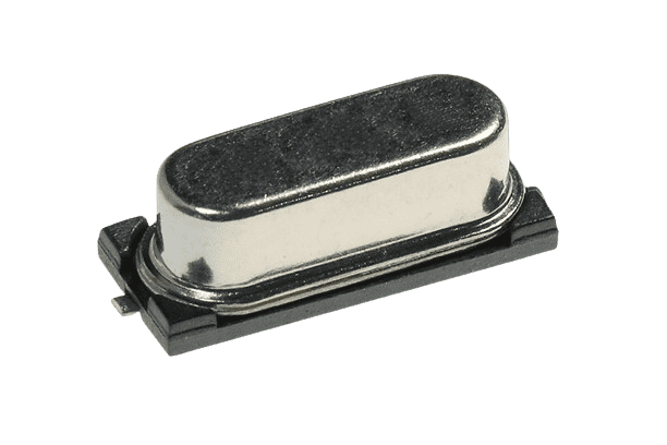
- Crystal 16mhz
- 3 leds
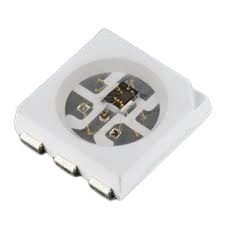
- Neopixel
- 3 Resistos 1k Ω
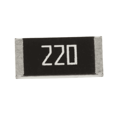
- 3 Resistos 220 Ω
- 3 Resistos 0 Ω
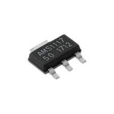
- Regulator 5v
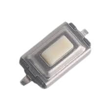
- 3 Buttons
- Diode
- Usb female
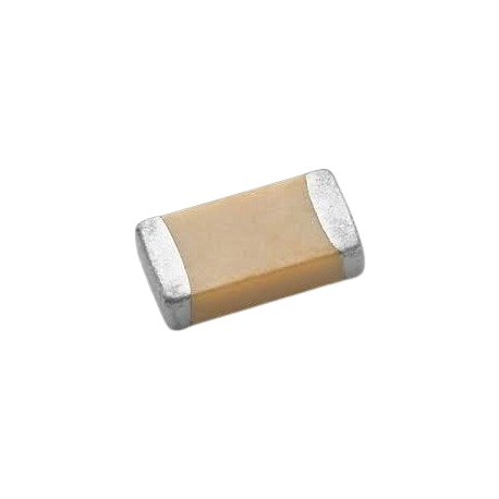
- Capacitors
- Header male 2.54
- Header female 2.54
Schematic
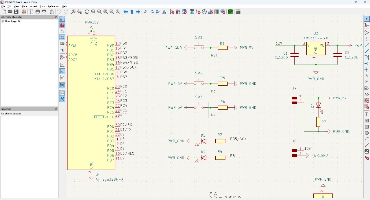
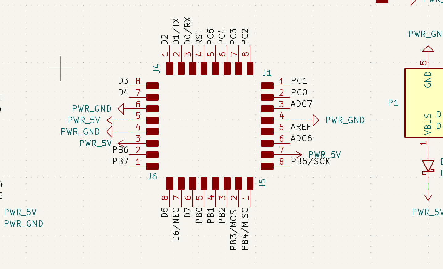
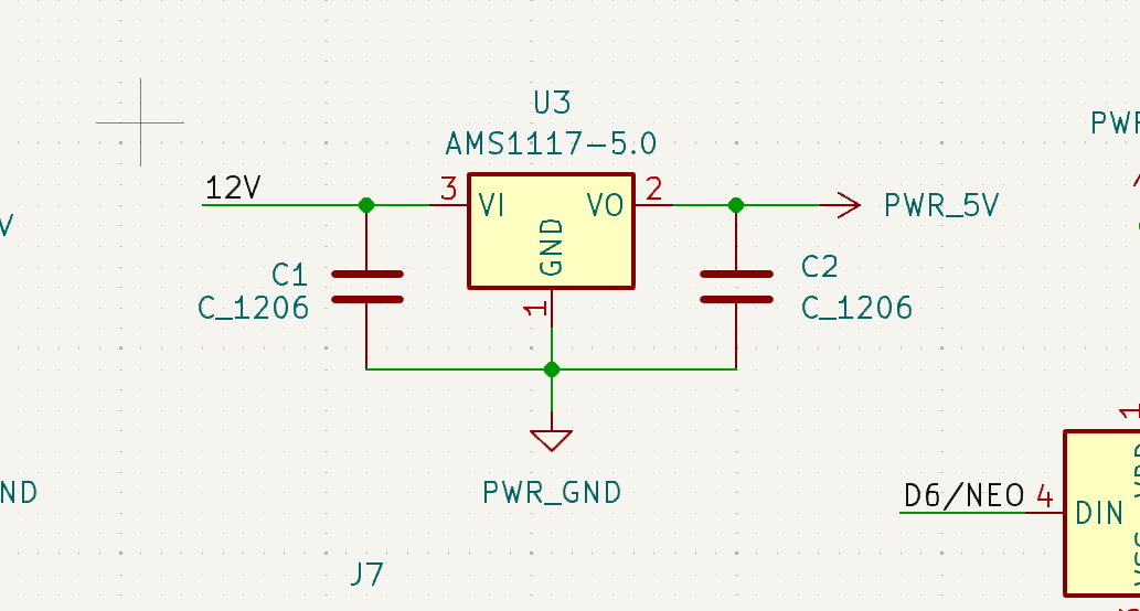
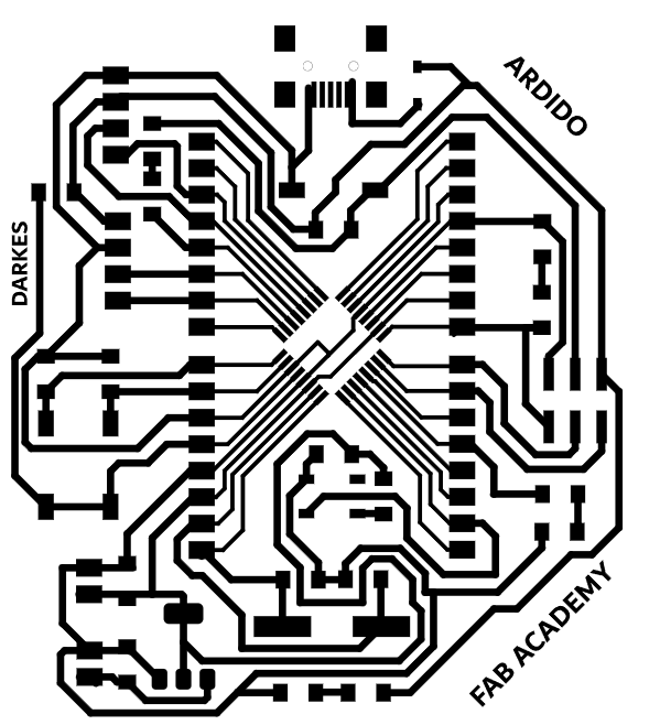
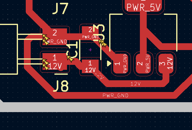
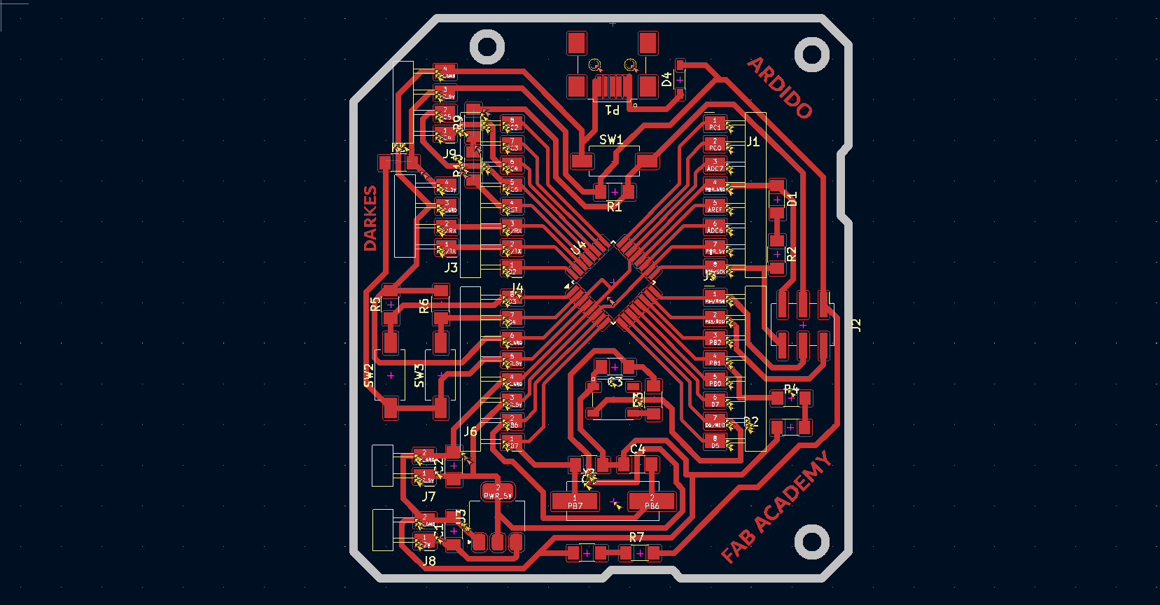
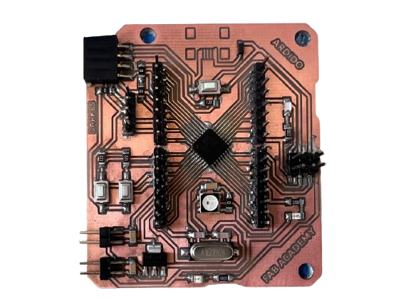
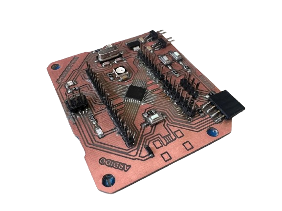
This is the design of my schematic; in it, you can see different blocks and different types of connections arranged. I chose to use labels because they make it easier to visualize and there are not so many intertwined wires. On the left, you can see the microcontroller with all its pins, on the right are the connections for the buttons and LEDs, and at the bottom, you can see multiple output pins in the form of the microcontroller. On the right side, you can see the voltage regulator, the NeoPixel, zero resistance, the crystal, and the USB.
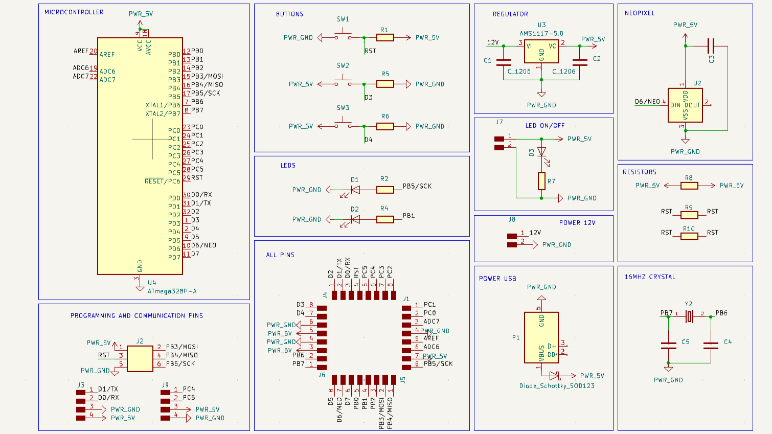
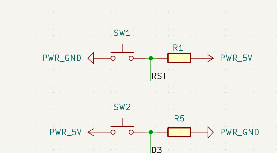
Using the symbol tool, I started adding the components required to do my work. Additionally, I used the label tool to name each of the pins I used, including 5V and GND.
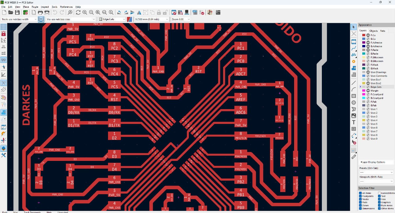
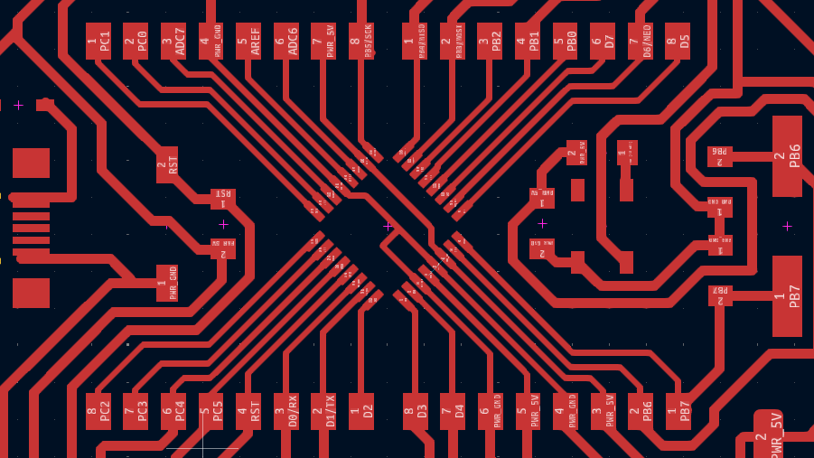
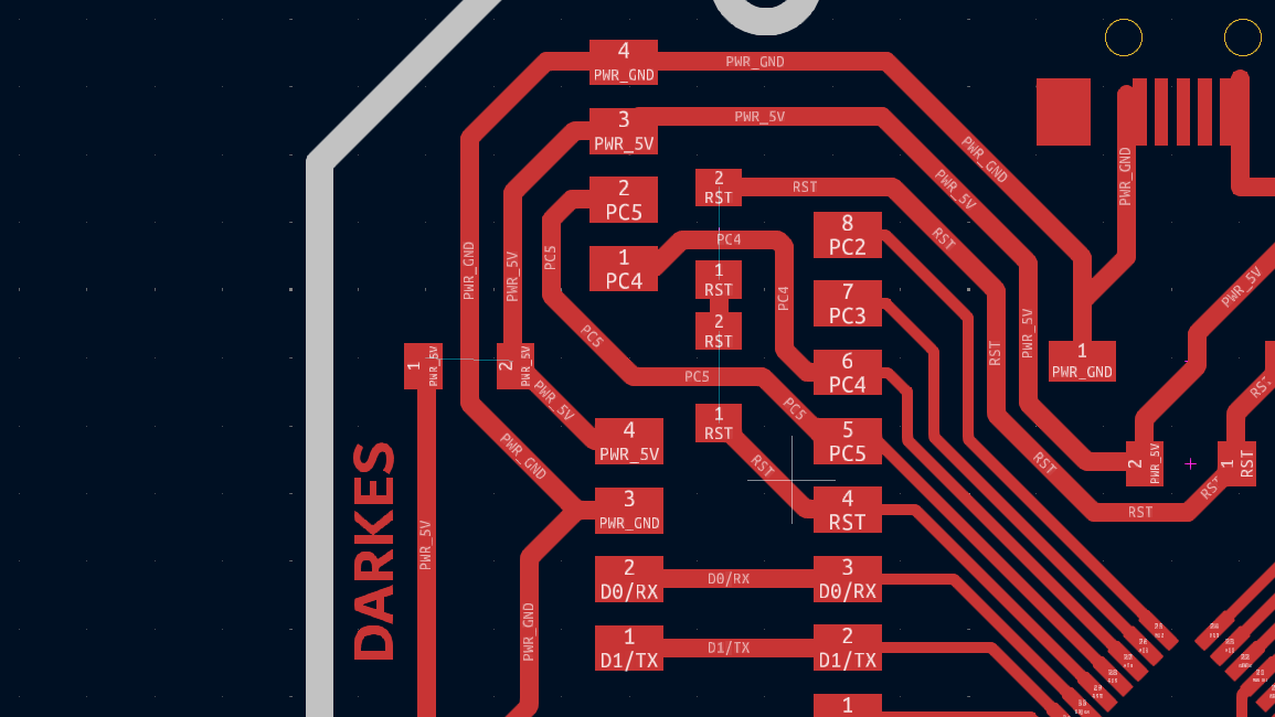
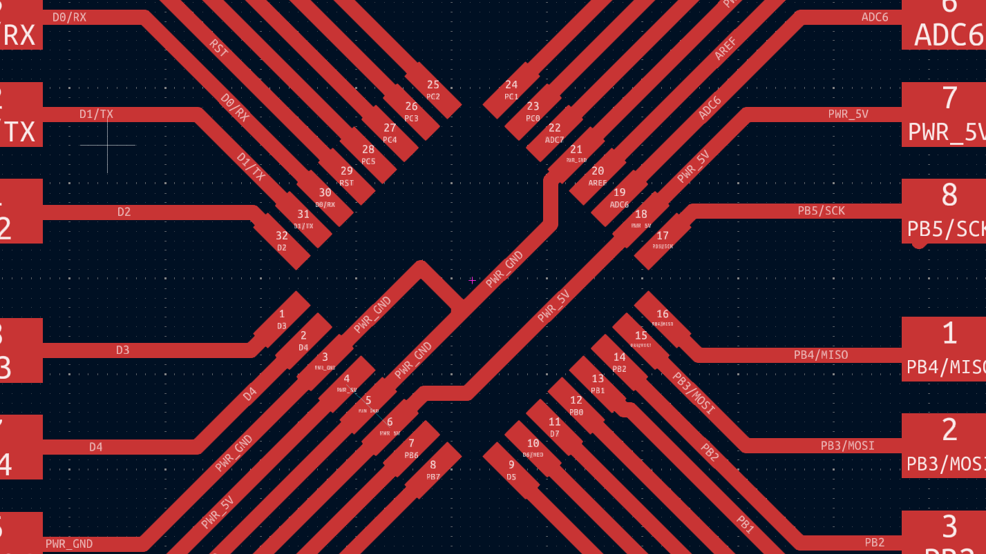
PCB
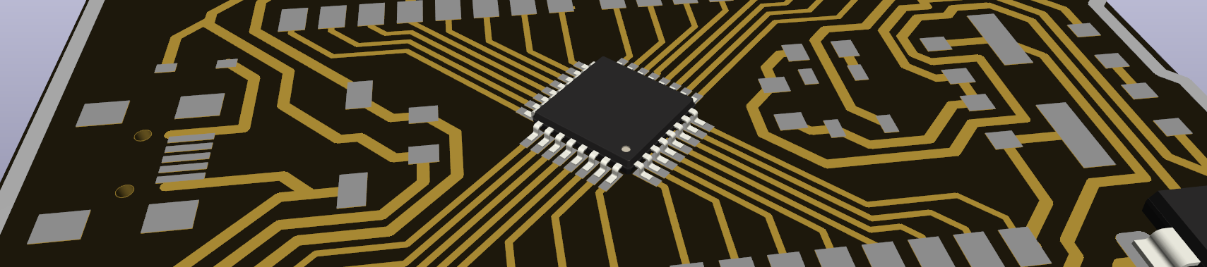
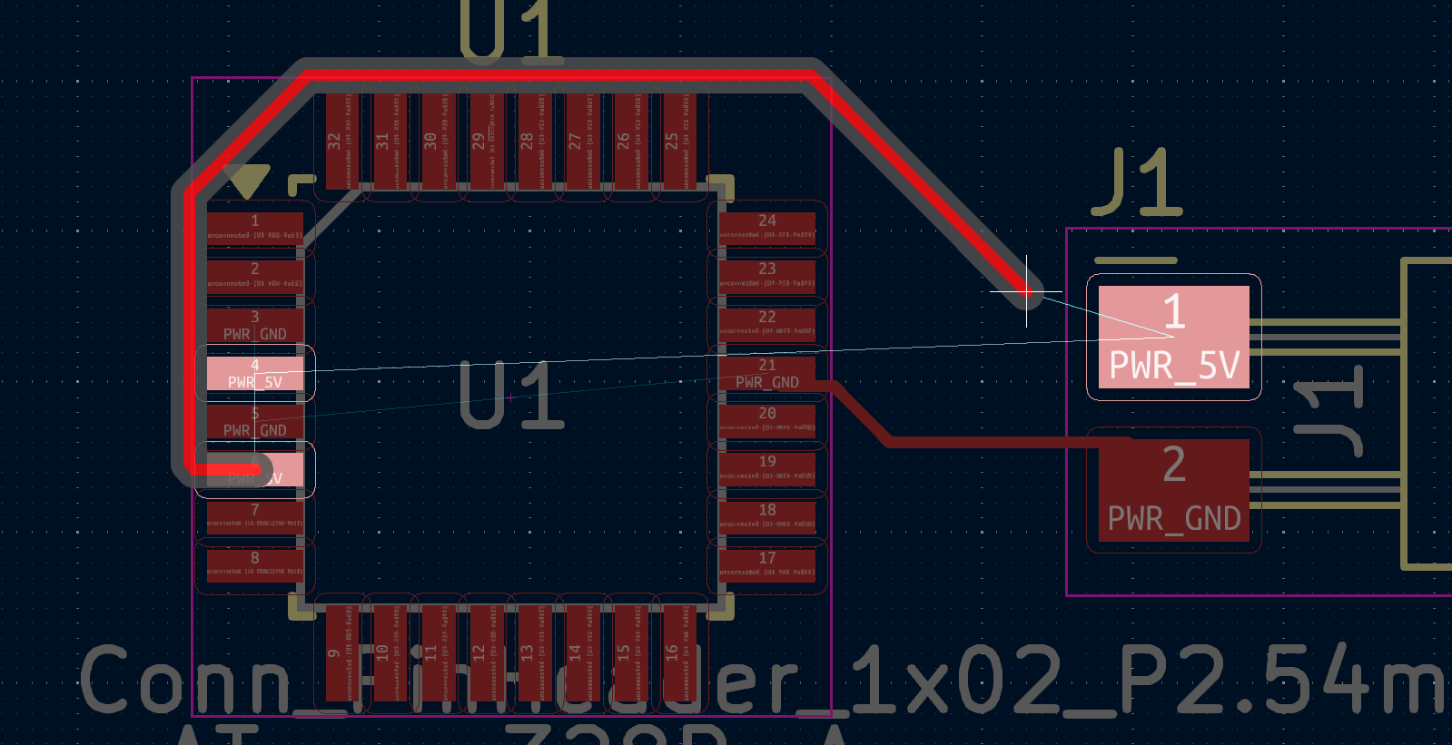
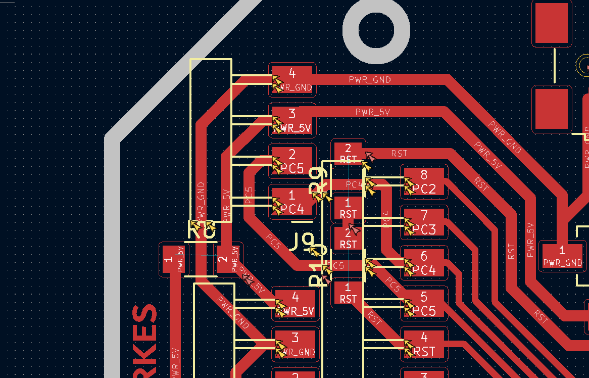
Here you can see the final design of the PCB. This design strategically places all lines and connections on the same side, ensuring that they do not touch each other, which is crucial for avoiding short circuits. The image displays various functional areas of the PCB, including the microcontroller with all its pins labeled
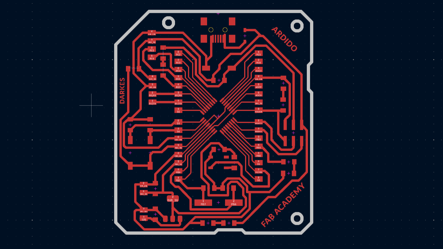
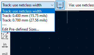
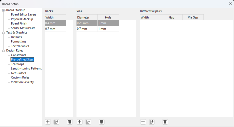
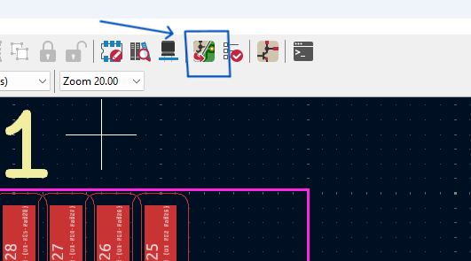
In the PCB mode, at the top left, there will be a menu where we can set the rules and measurements to create profiles when connecting our components. Within this menu, we can create different profiles if required for the creation of the PCB. These are the measurements I used for this design.And every time you make a change in the schematic, you will have to export the changes with the button that is shown.
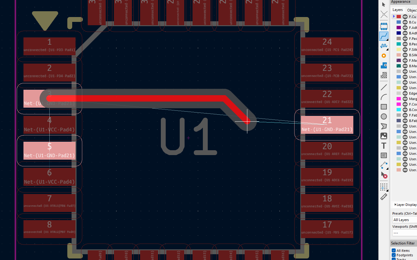
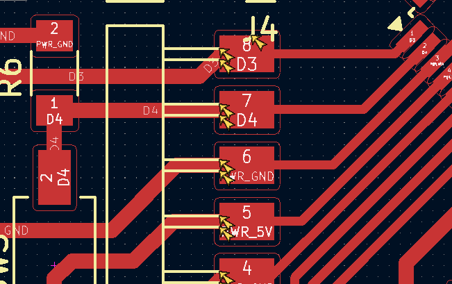
With the wire tool or by pressing the X key, we can connect the components. We can only connect the same components that have the same label as shown below. With the help of this tool, we can make all the connections on our board.
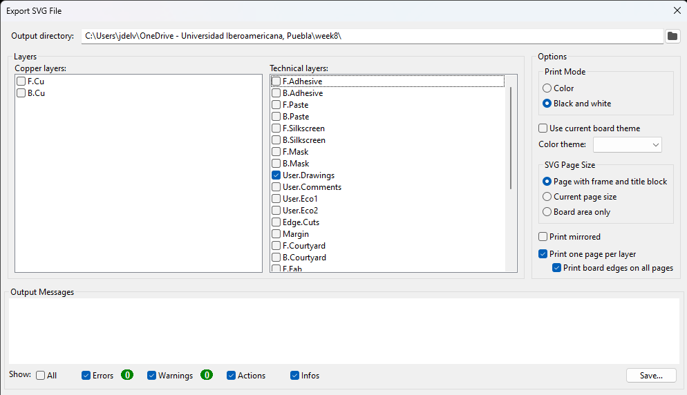
Once the PCB is designed and a border is added on another layer, export the PCB as follows: Export, SVG. In the window that appears, select the trace layer and then the cut layer to export.
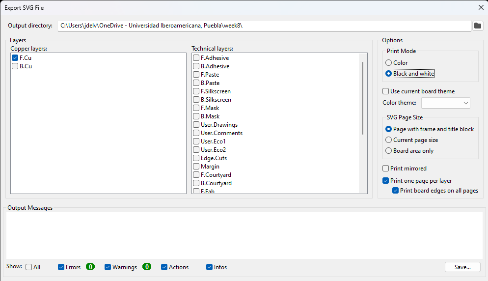
Once the SVGs are exported, you will have the following traces. These will be transferred to the Mods program, which will generate the manufacturing program for the PCBs. Check the previous week for more details. DOWNLOAD PCB
DRC process
The DRC (Design Rule Check) process is a critical stage in PCB and semiconductor chip design. It involves reviewing the design to ensure it meets specific manufacturer or fabrication process rules. This process checks aspects such as the spacing between traces, the size of traces and pads, the correct dimension and placement of vias, and the space for the solder mask. The goal is to identify and correct errors before fabrication, thereby avoiding costly rework and reliability issues in the final product.
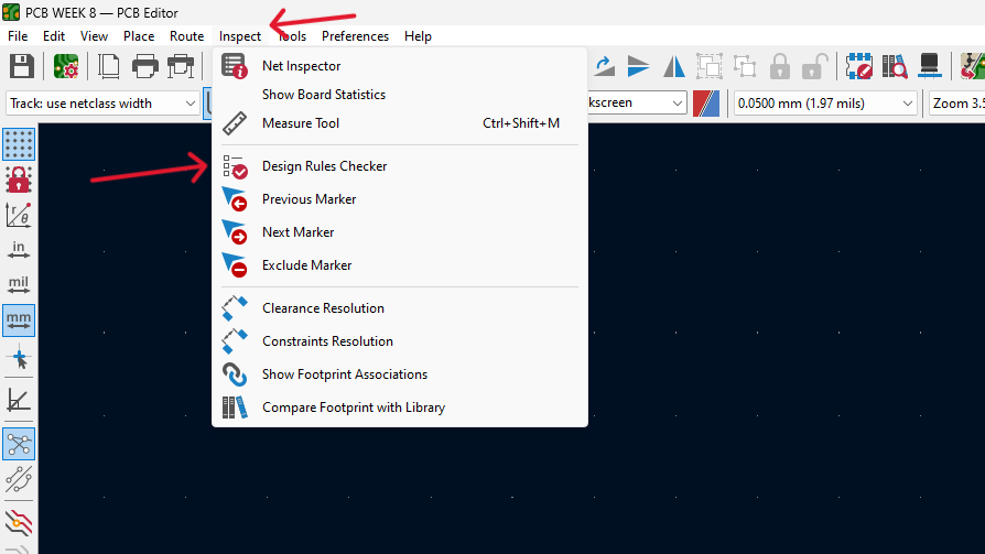
To perform a check, go to the menu Inspect-Design Rule Checker. Press the Run DRC button to display all possible errors.
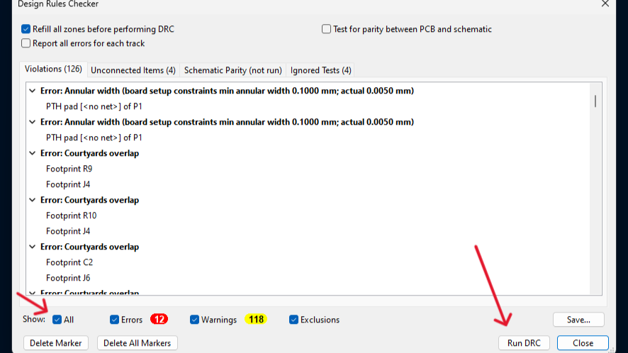
In my case, it showed many errors of overlapping tracks and pads, as well as certain tolerances reaching the minimum separation. However, upon visual inspection, they didn't seem to be a problem.
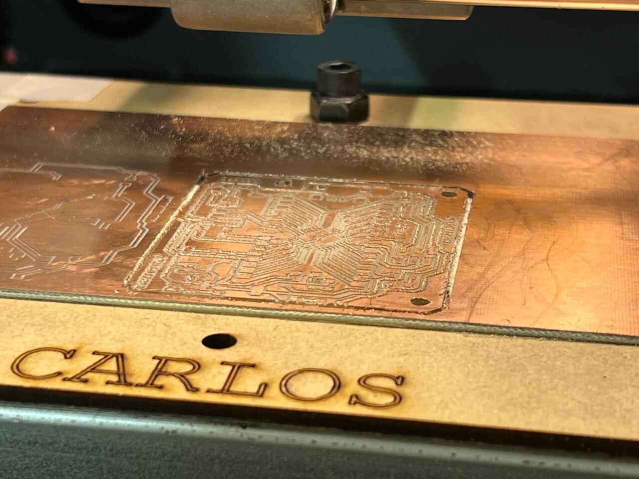
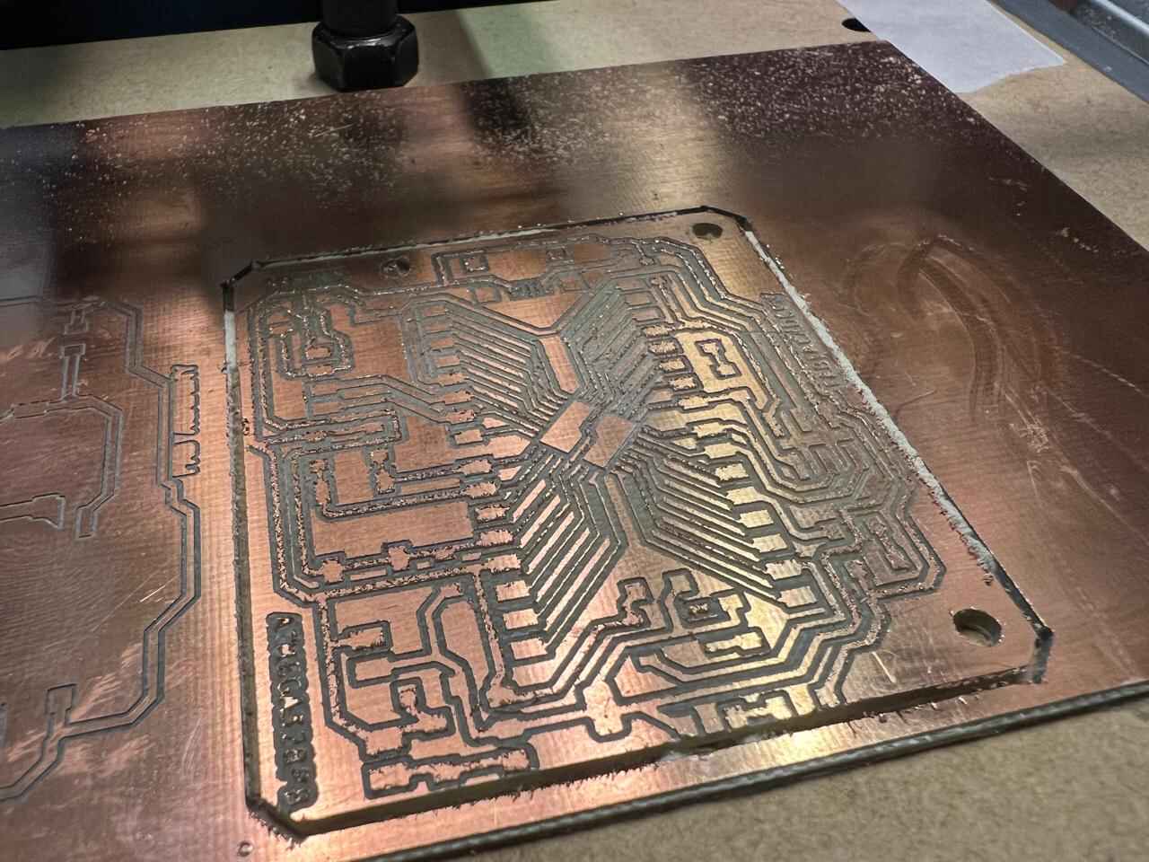
fabrication
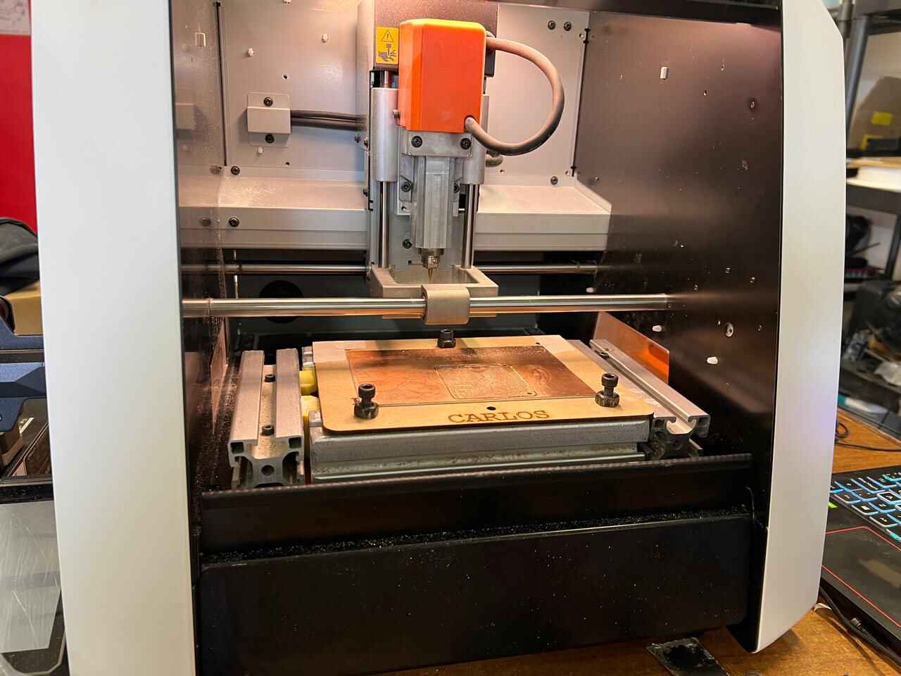
For the manufacturing of the PCB, I used the same manufacturing process as in week 4 of this page. Using the SVGs and the Mods program, I created the file to manufacture the board. Subsequently, with the help of a soldering iron, I soldered all the components to get the board operational.
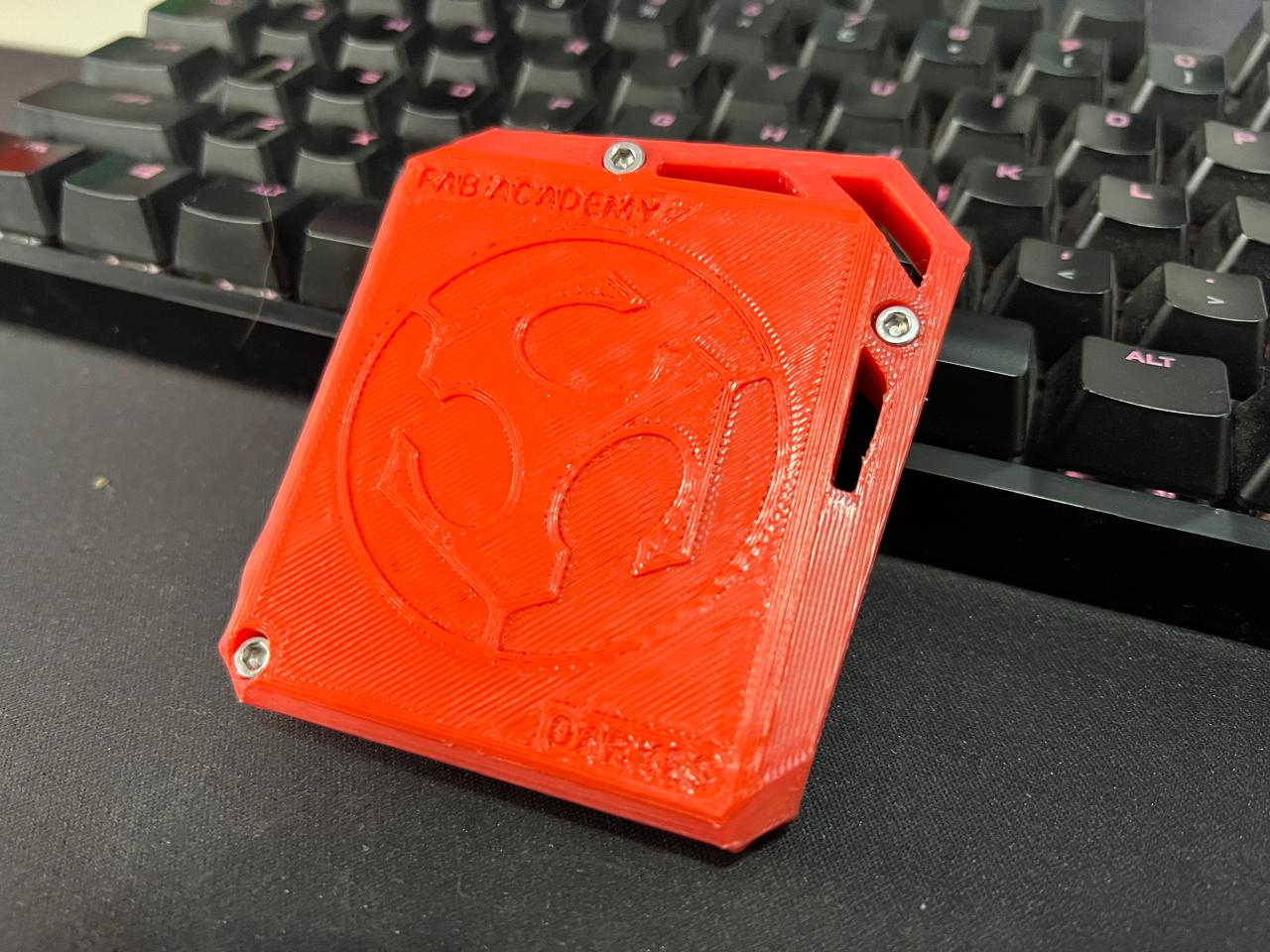
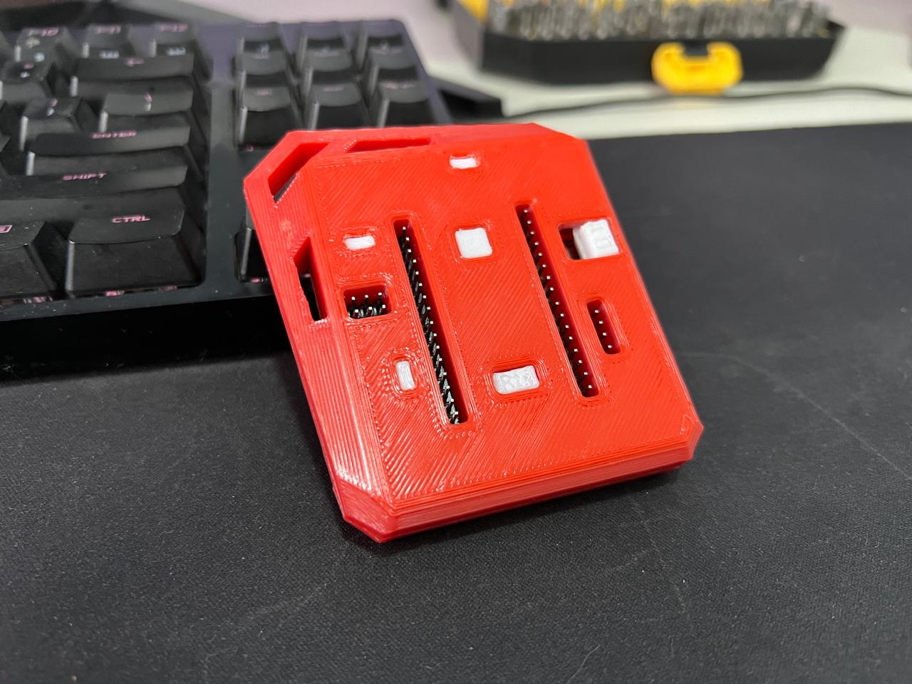
printed case
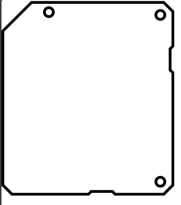
For the design of the case, I aimed to create a design that completely covers the board, allowing me to transport it easily and carry it in a backpack. Additionally, the case includes buttons that facilitate pressing the buttons on the board. The design features a hole through which I can pass a string if needed for easier transport. The case is screwed together to enhance its durability and resistance. DOWNLOAD CASE
Testing
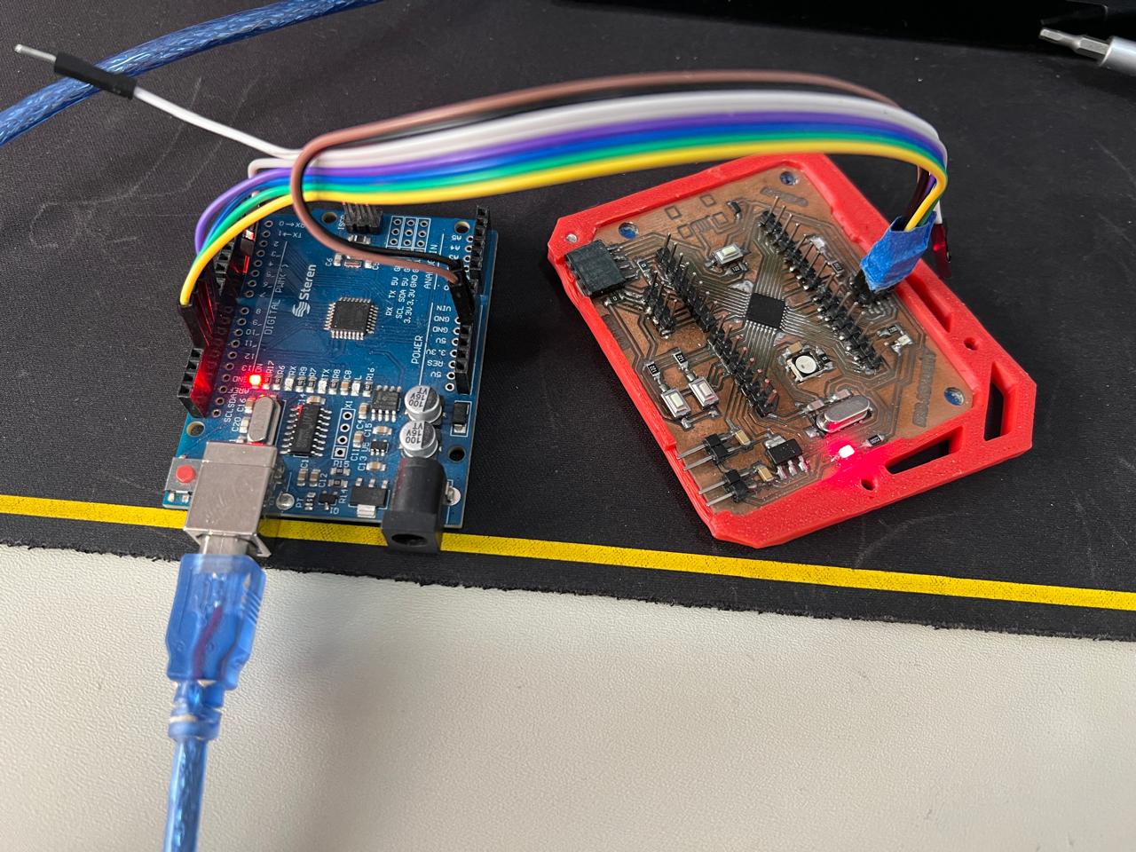
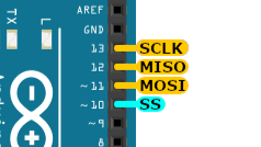
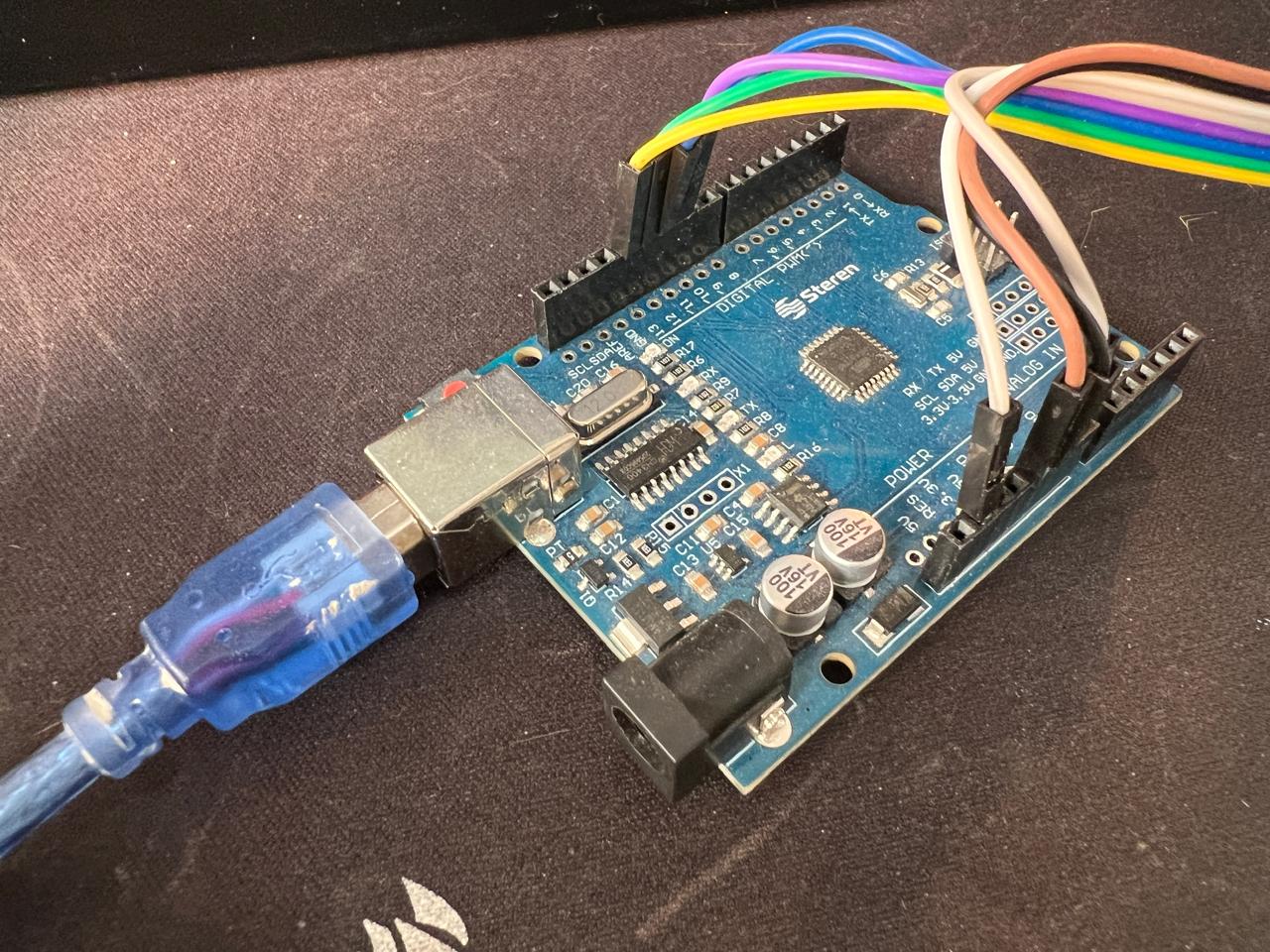
For programming this board, I will use an Arduino Uno and the SPI communication protocol for its connection. These pins are already located and separated within the board. Arduino already has a sample program to convert your Arduino into an SPI programmer.
The SPI (Serial Peripheral Interface) protocol is a communication method between devices where one master device controls one or more slaves. It uses four main lines: a clock line (SCLK) for synchronization, a data line from the master to the slave (MOSI), another from the slave to the master (MISO), and a line to select the slave (SS). It is fast and commonly used to connect microcontrollers with sensors and other peripherals.
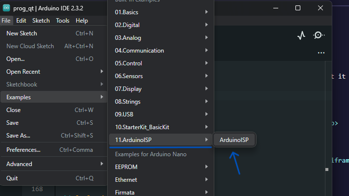
Here you can see where you can find the program. Example of Arduino and SPI to be able to load it and subsequently program another microcontroller with it.To convert our Arduino into an ISP programmer, we just need to upload the code and make the connections including 5v and GND.
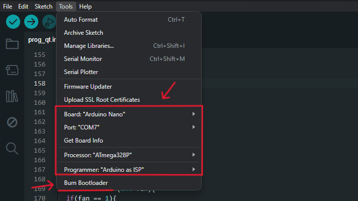
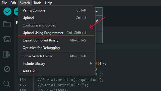
With the Arduino ready as an ISP programmer, I continued with my manufactured board. Before programming, we need to burn the bootloader onto the board. This way, it will be programmable. I ensured that the configuration parameters were correct, as shown in the image, and pressed the "Burn Bootloader" button. Once it is loaded, it will be ready to be programmed to upload the codes. We will then move to the next menu and select the option "Upload Using Programmer."
The code I will use to test if my board works is a sample example from the NeoPixel library, as I am currently only interested in being able to upload code to my board. DOWNLOAD CODE