

8. Electronics Design
For this week´s assigment, we are creating our own PCB with microcontroller from scratch. From designing the schematic to testing its functionality.
Extra information about electronics design is available a the Electronics Design Fab Ibero Puebla´s Page
But for a quick introduction, these are the most important parts of creating a PCB are: selecting your components (and also making sure the component is the right size, since components like resistors have different sizes, even surface mound), making the connections between them as this will later become the tracks, adjusting all your components so they fit inside your PCB, and lastly, placing the tracks that will connect each component to each other.
For this, we will need to use an EDA; Electronic Design Automation. There are a bunch of softwares like this kind out in the internet, like Altium, Eagle, and Kicad, but the one I like and the easiest for me is EasyEDA, you can download it using This link, select your client in the Std Edition.

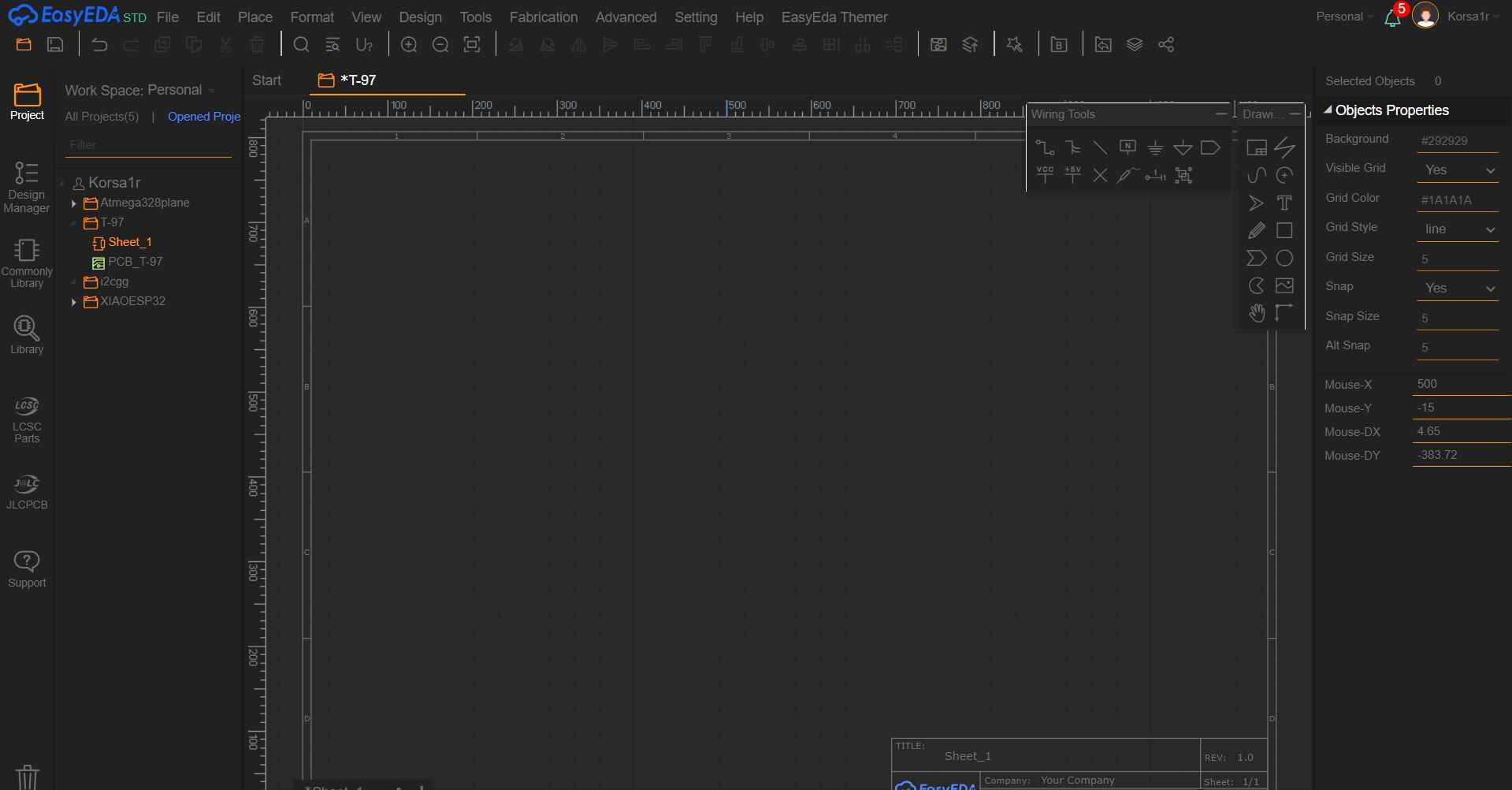
Once in, open a new project and then a new schematic, it should open a blank canvas like this:
For my design, I will be doing a different version PCB for the XIAO RP2040, so we need the part and footprint of it to design our PCB around it. To do this, we can go to the Library tab on the left menu, and type XIAO
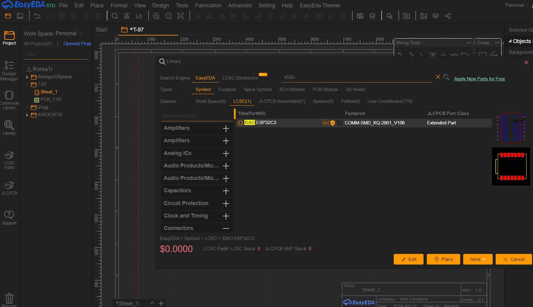
As you can see, the only part showing up in the search is technically a XIAO ESP32C3, but it actually has the same footprint and the pins are in the exact same position as in the RP2040, so we can use it regardless.
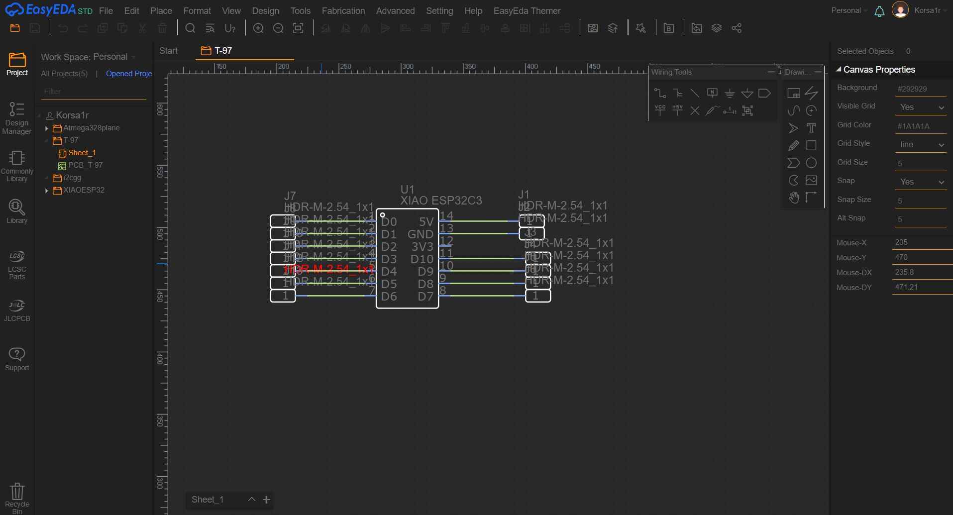
Once we have the XIAO, I will only put pinheaders on each port (except for the 3v since I will not use it). For this, we can go the common library also on the left menu, and chose which type of pin header we will add. You can chose between 1 individual pin, 2, 4, 6 and possibly even more terminals together, but since I want to put each pin header separately, I will put the individual ones to each terminal.
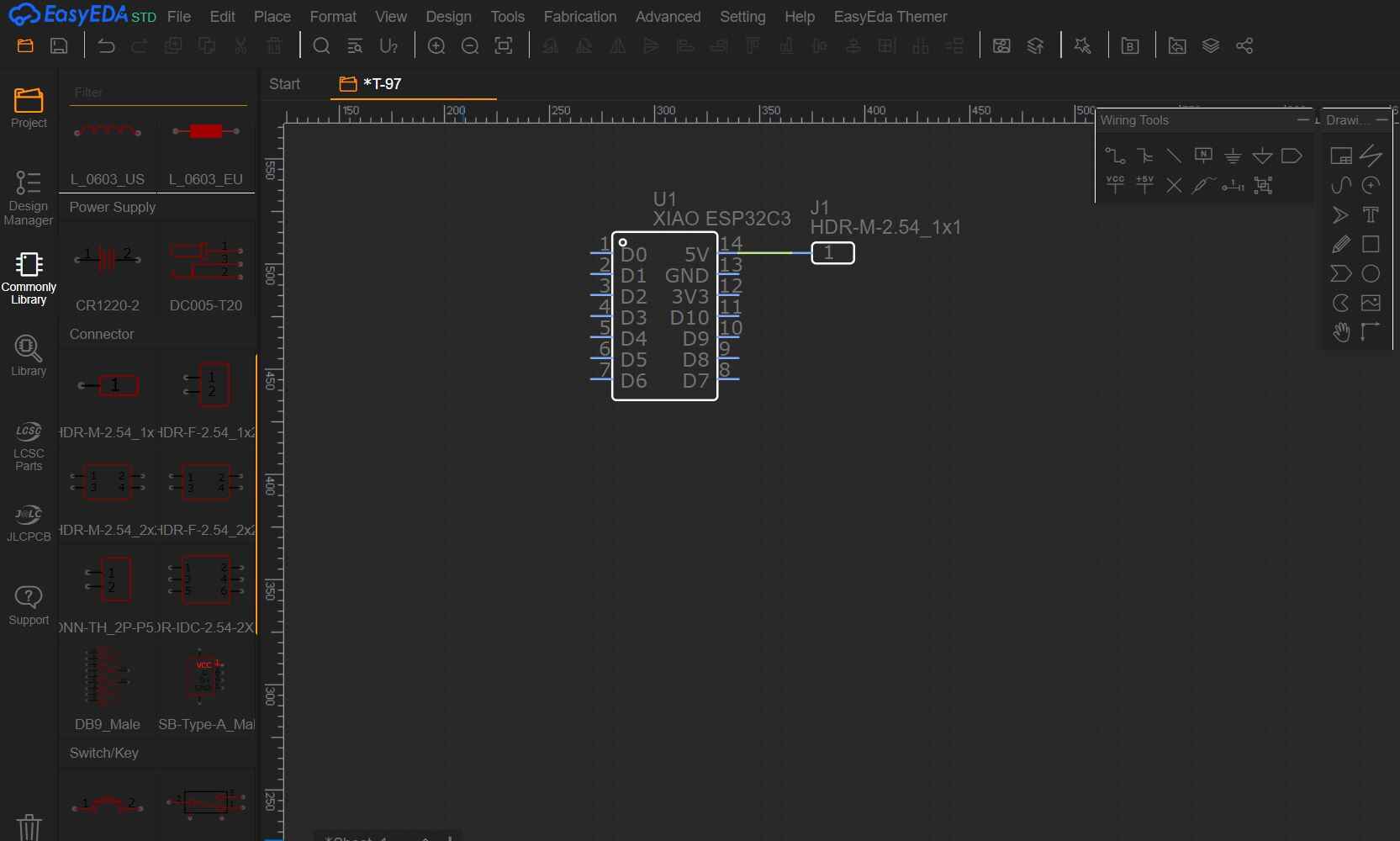
To connect the terminal to the microcontroller, press "W" and join the 2 nodes you wish to connect, and we do that with all the pins
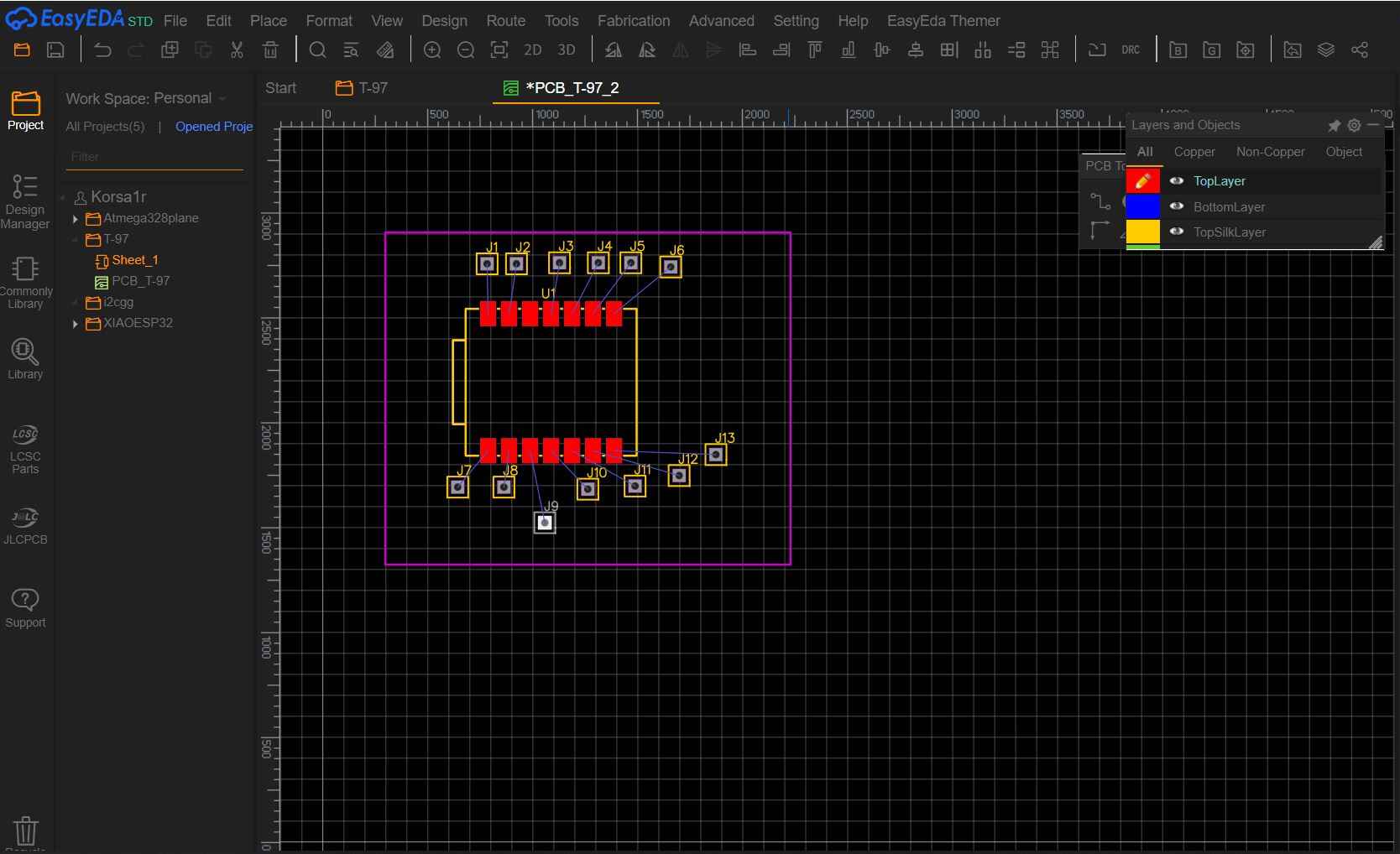
Now, save your changes, and on the top menu, select Design -> Convert schematic to PCB. If there is a warning note about unfinished nets, just click "keep going".
Once in, all your individual components will be scrambled next to a purple rectangle, you will also see a thin blue line between each component and the place it should be wired to. This is a very usefull guide to help us connect each node to it´s respective one. I sort of arranged each one in it´s preliminary position.
Again, press "W" to join the respective nodes to it´s respective position. Using the blue line to guide yourself between the components.
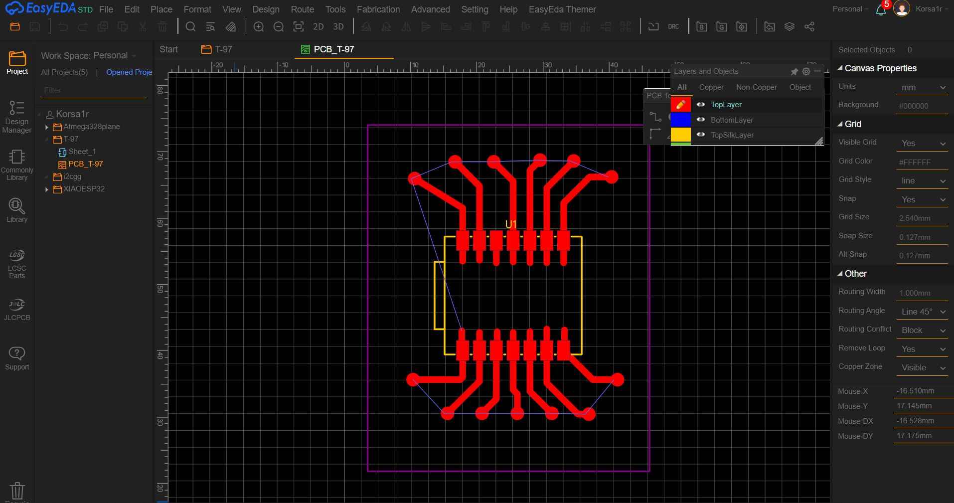
IMPORTANT NOTES: 1) The default track width is very thin, and can compromise the entire build of the PCB as it can easily break or be incorrectly carved in your machine, so the width that worked for me was between 0.8-1 mm, since my design is very simple and I do not have cramped spaces between components, I can do 1mm comfortably, but if you have space issues you can reduce the track with but I would not recommend going below 0.7 mm, as you might compromise the integrity of the tracks. Although, the width of your tracks should depend on the amount of current that will be going through that track, the more, the wider it should be. In my case, we are not using a lot of current, or at least not enough that it will be problem with the tracks, so I am focusing on ease of creation, but when using high power components, you should have in mind the thickness. You can change the width by clicking in one of them and on the right side menu you get the properties menu.
2) You can also see that none of the tracks have a 90° angle turn. This is because it can cause issues like noise or electrical archs in the tracks, among other issues. In this PCB, it would probably be fine to have 90° turns, but it is good practice to do above 90° turns in your tracks, you will see that the software will naturally want to give you recommended track routes to avoid this exact problem.
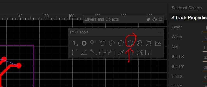
3) As you can see in the picture, I deleted the pin header components after making all the connections, this is because I added little circles around the tips of the tracks for an easier soldering. You can add those on the PCB Tools tab on the marked option:
4) Lastly, I stretched the purple outline to better fit my components, do so too to your liking.
Once happy with your design, we need to save both the tracks and outline separetly in an SVG format, we do that by going to File -> Export -> SVG. This will open a menu with a bunch of checkmarks:
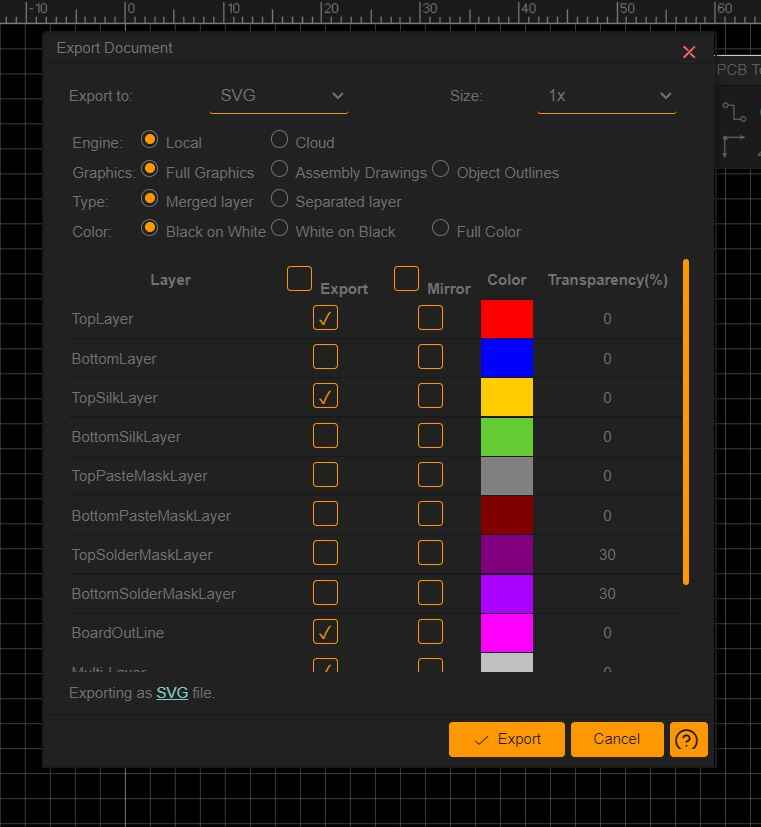
Firstly, unselect all the checkmarks EXCEPT for the red TopLayer one, and click export, yo will need to scroll down to find all the options. Once done that, do the export option again, except this time unselect all the checkmarks except for the purple BoardOutLine and once again save it.
The next step is to create the RML files out of the SVG ones we saved, we do the same procedure in MODS as we did in the Electronics Production week.
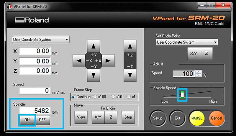
This time, we are using the ROLAND SRM-20 cutter for our PCB.
This also means we need the VPanel software to run this machine. You can download it using this link.
Note: This software will only open if we are connected to the machine. But once we do, the menu should look something like this:
Note: If even while connected to the machine, the menu does not appear or an error message shows up, make sure you have all the drivers installed, they can be found at the VPanel download page on the left side menu. I could not access the software until I downloaded and installed the drivers.
Now, we need to set the zeros for our machine to cut. Meaning we need to place to place the tip of the drillbit (a 1/64" ponted drillbit just like we did on Electronics production). But first we need to set our copper laminate to our sacrificial plate.
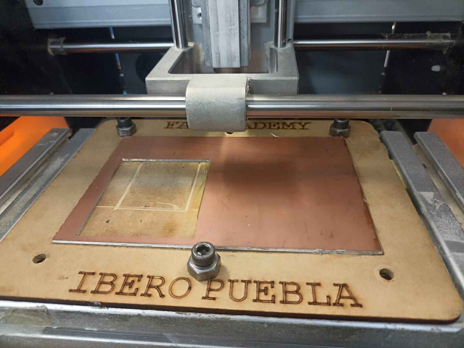
To hold the plate to the MDF, we use once again doble sided tape on the backside, and the 3 screws hold the plate to the machine.
So using the menu, we move the drillbit to the bottom left most side of the plate that we can use, as you can see, mine had a previous cut from another PCB, so we set the X,Y,Z, zeros just to the bottom right corner of the other cut.
This is not the exact same laminate, but it should look something like this, barely touching the bottom left corner:
Note: For a better result, click on the "ON" button on the spindle, and wait for the number to reach around 9,000 rpm´s, this will allow you to lower your tool to the desire height without risking breaking your drillbit. It also gives you a visual cue, as you should lower your drillbit until it barley starts drilling and eject white dust.
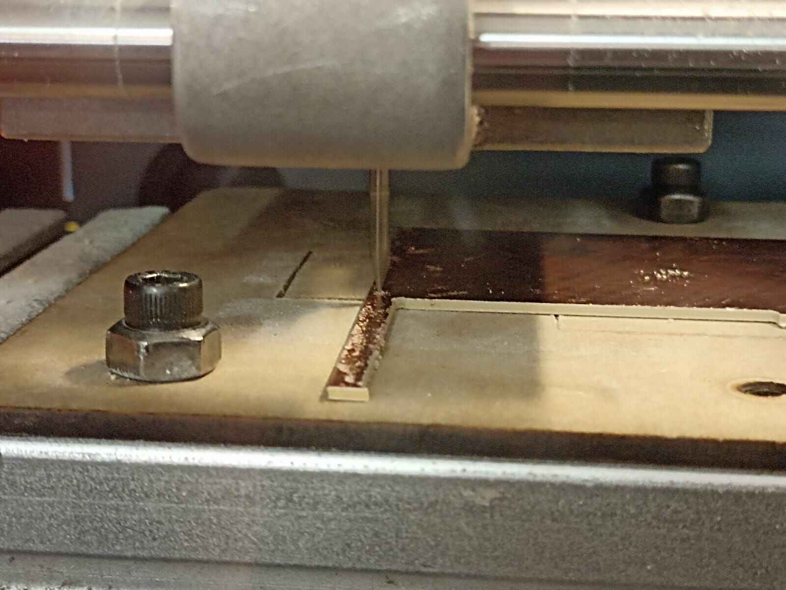
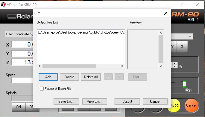
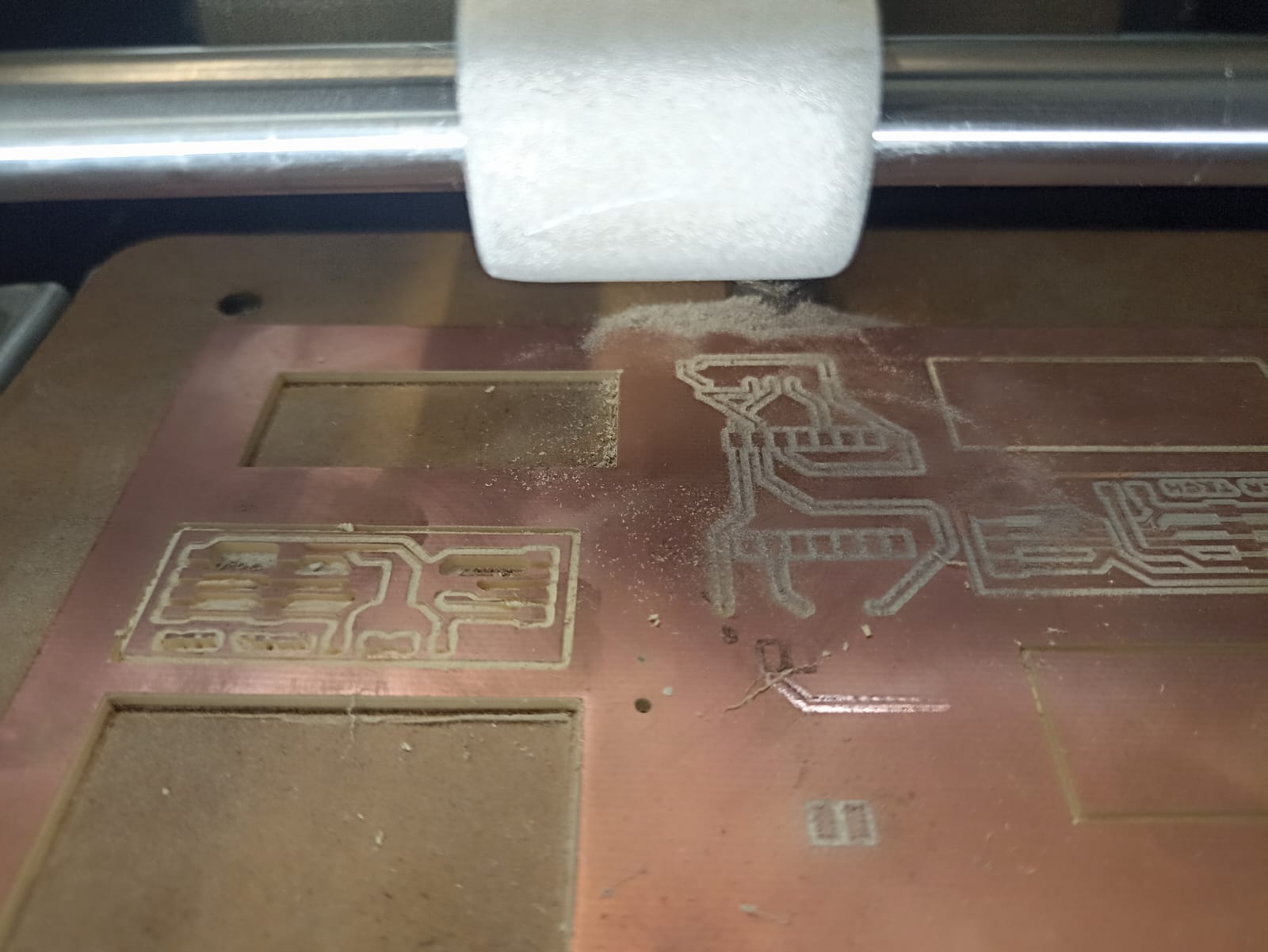
We then press the "Cut" botton on the menu, press "Delete All" if there is a previous file on the list, click "Add" and select our tracks RML file we did on mods, click on "Output" and it should start cutting.
Once it finishes, it should look like this:
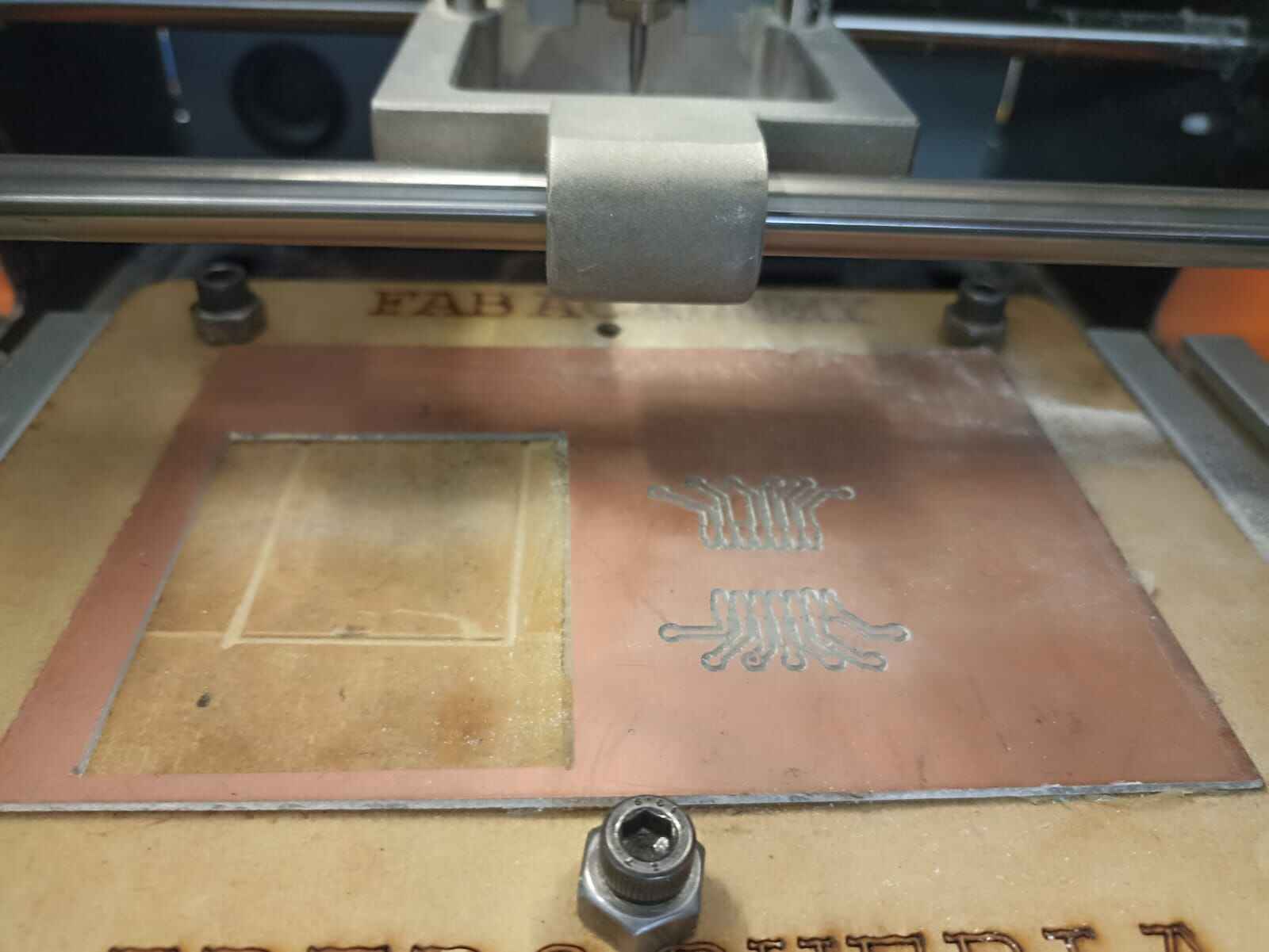
Remember: the white dust residue is very toxic to breath in, so make sure to vaccum it once the machine has stopped.
Now, we need to change the tool to the 1/32" drillbit to cut the online. Important: change the Z zero so it is barely touching the plate, but do not change the X/Y zero, since it is already aligned with the PCB, and a change in it would case the outline to be cut in a different position than we want and ruin the PCB.
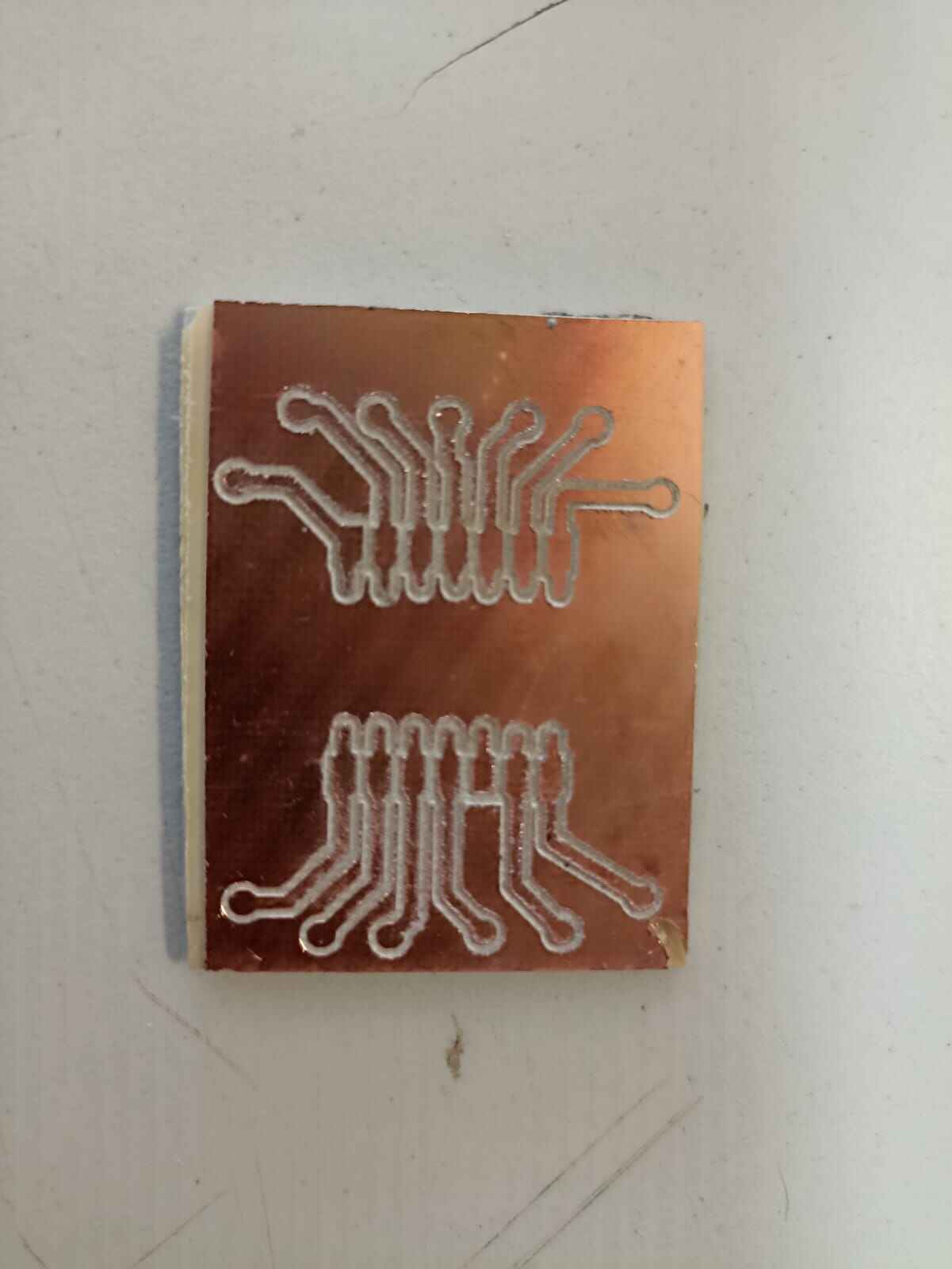
I unfortunately lost the footage of the outline cut. But it came out looking something like this:
Note: I often saw that when using the 1/32" drillbit to cut the outline, sometimes the copper laminate would unstick from the MDF and would be damaged. This happened to me and to other classmates. Once solution I found was to use regular tape to hold the borders to the MDF, so it would be harder for the plate to unstick.
We solder the XIAO on top:
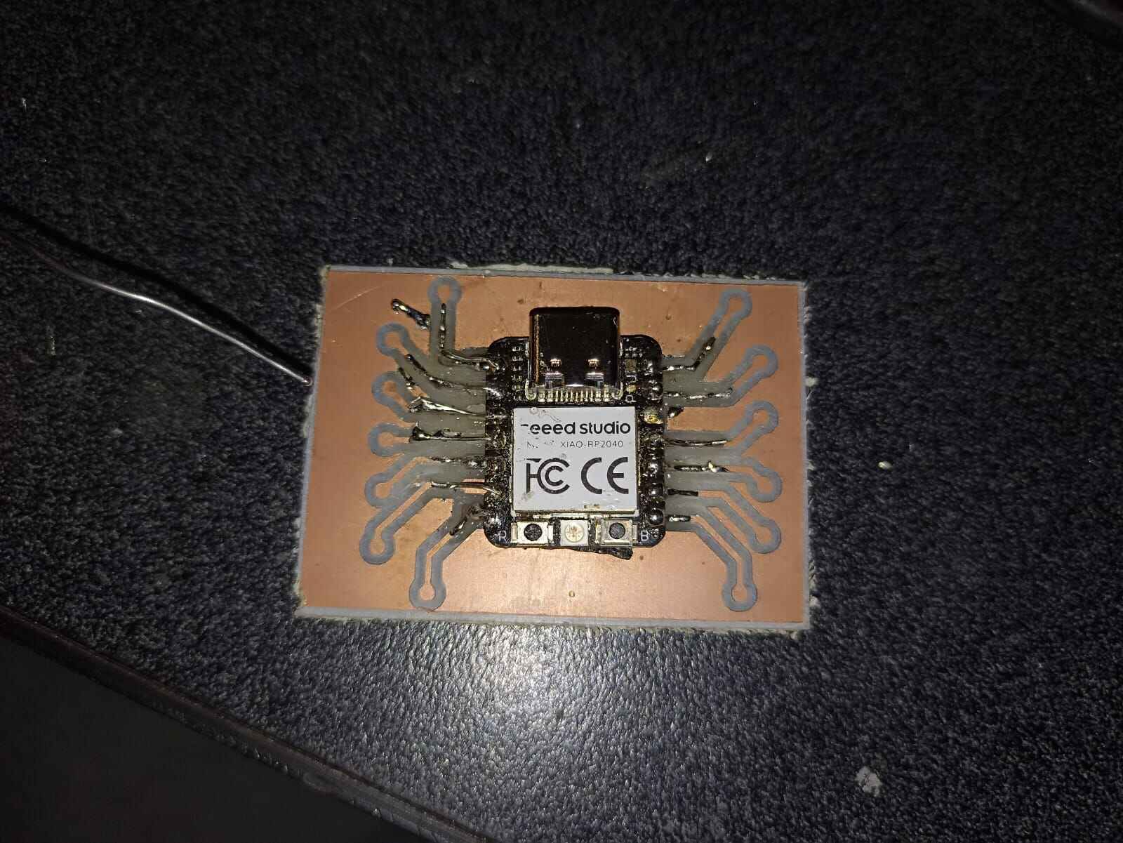
After that, we solder the pin headers to the ends of the tracks so we can connect cables to it in an easier way:
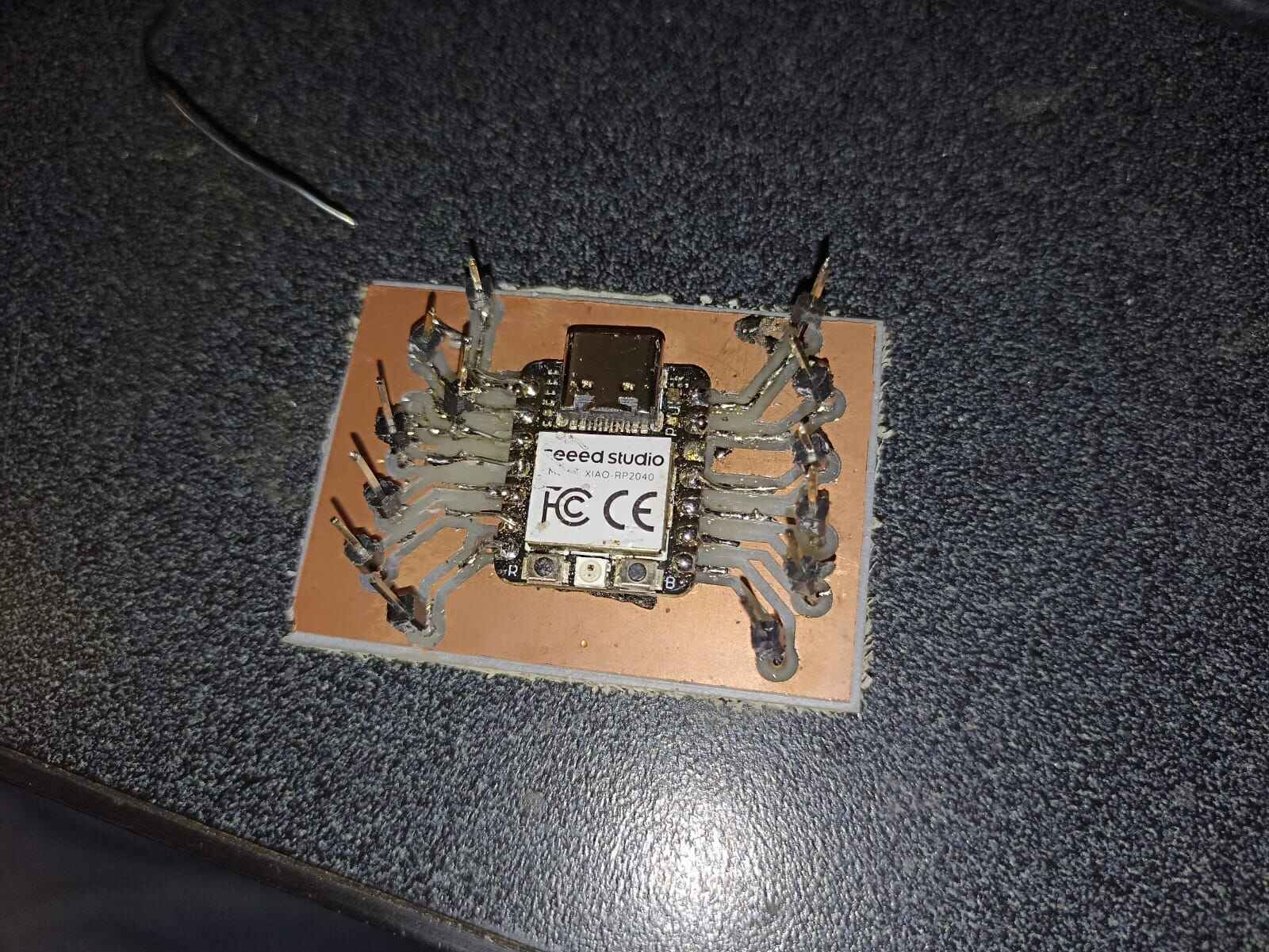
Now that I look at it, it looks a lot like a spider or a bug. I´m arachnophobic so it makes me somewhat uncomfortable...
Nevertheless, let´s test it! Im gonna do a simple blink test with a Led and a 330 ohm resistor to the pin 29 as you can see on the diagram below. We open the Arduino IDE, make sure we have this board URL on our preferences: https://github.com/earlephilhower/arduino-pico/releases/download/global/package_rp2040_index.json and run the following code:
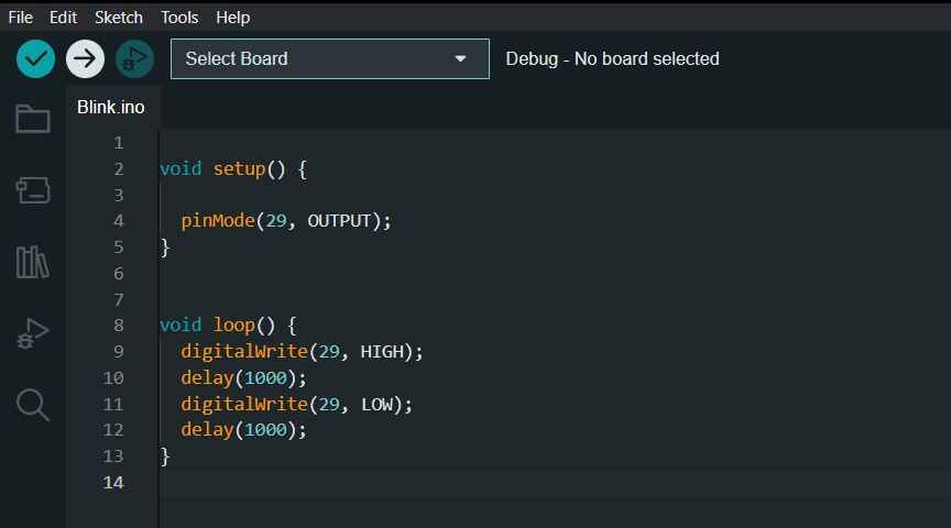

As you can see in the pinout and the code, I connected the positive side of the Led to the Pin P29 and the negative side to GND, and it blinks in 1 second intervals.
Multimeter
Note: When creating your own PCB´s it´s not guaranteed that your system will work, and when it doesn´t (trust me, someday something will fail), you need to identify what part could be going wrong. That´s why multimeters are such an important tool when designing and prototyping. The proper way to measure something like resistance is the following:
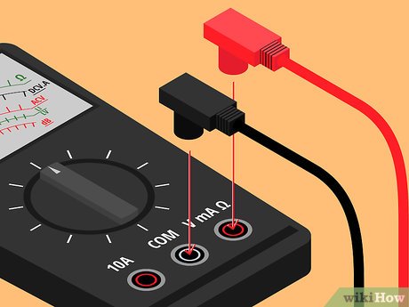
To start, make sure that your probes are in the correct intake: black goes to ground (or COM), and the red one should go to wherever the resistance symbol is. Most, if not all, multimeters have this pin at the right side, where other things like voltage and continuity are measured, using the other intake will not give us a measurement of what we want.
Then, select the resistance slot, which is represented by the omega symbol "Ω".
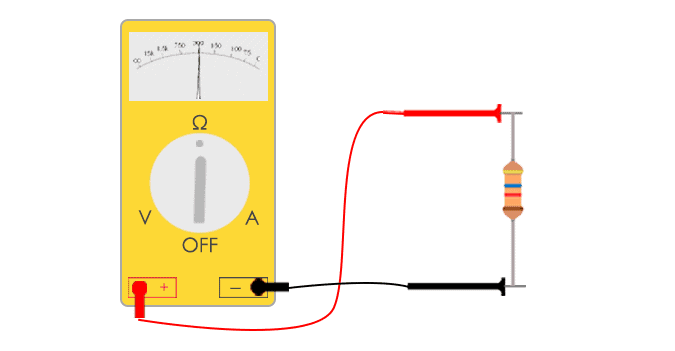
Lastly, to accurately measure resistance in a specific part of your PCB, place your probes between both ends of the resistor, sort of "parallel" to it, as shown in the picture:
This should give you a reading on your multimeter. Note: Be careful, as the number given in the display may be the true value, or could be in kiloohms or megaohms, check the prefix on the right side of the display for a "k" or "m".
Second PCB
Now let´s make something a bit more robust. I want to add a surface mound led with a button, and a potentiometer to test servomotors. So just like before, we do our schematic:
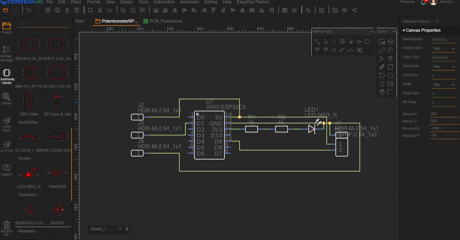
As you can see, on the 3.3 volts output, I have a space for a button and a resistor for the led. 3 pins for the potentiometer going to voltage, analog signal and ground. And on the other side 3 pins for the servomotor.
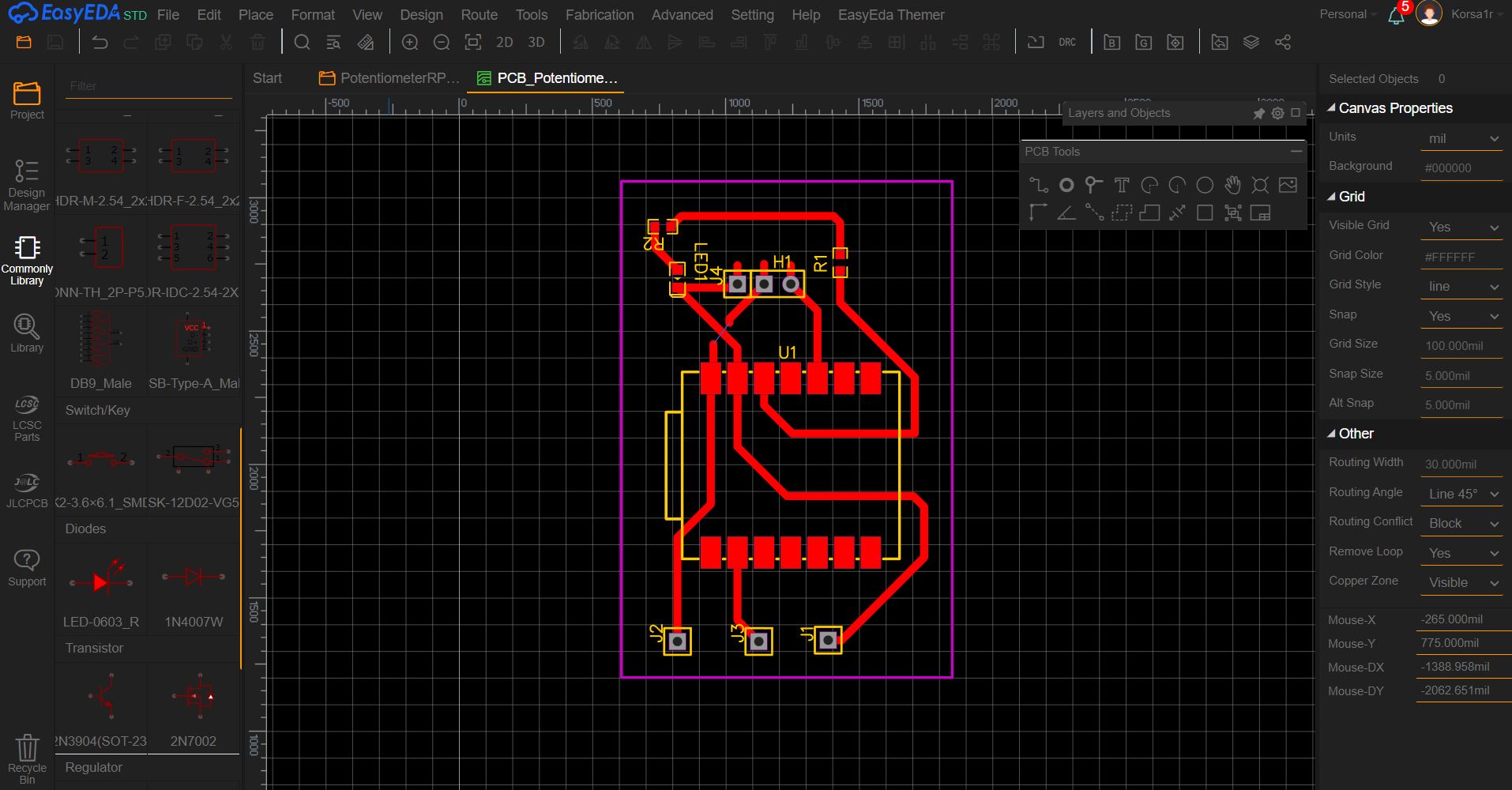
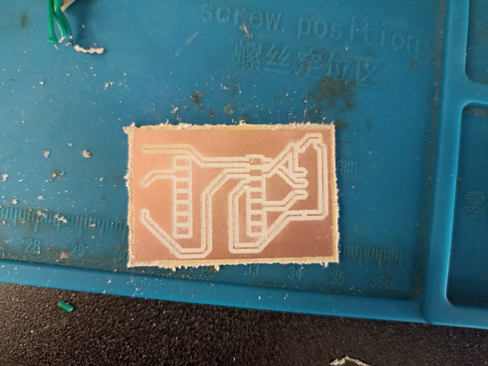
And here we have the PCB of the diagram. Note: Firstly, I had to turn the whole PCB 90° so it would fit on my copper laminate, also there´s a little gap in one of the traces since I could not connect everything in one layer
We do the same process as before and do the traces first on the cutter:
And then the outline to cut the individual PCB out of the laminate
The components for this PCB are the following:
- 5K Potentiometer
- SMD LED
- SMD 270 ohms resistor
- SMD Push button
- 3 Male Pinheaders
- XIAO RP2040
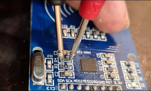
Here´s me soldering the resistor :)
After all the components were soldered, this is how it looks like:
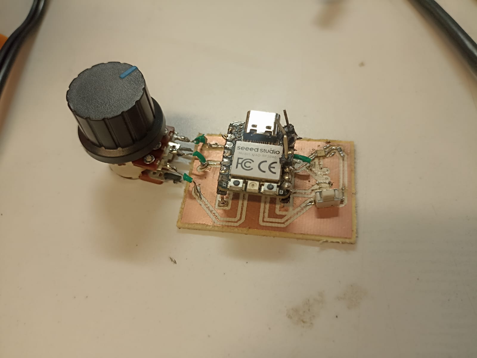
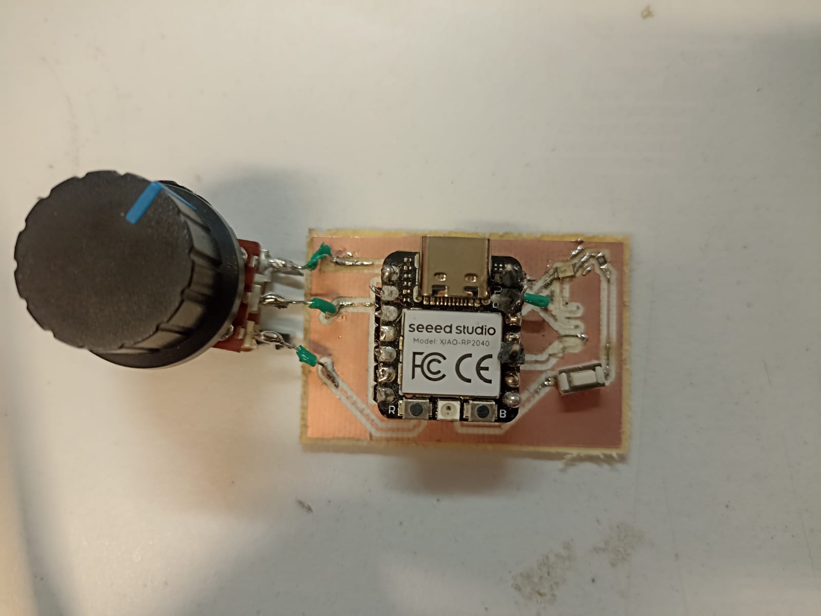
Note: When I was soldering the pin headers for the servo, I accidentally took out the traces, and therefore could not solder them in their respective place. What I had to do to test the PCB was to solder them directly over the XIAO´s pin, they are definetly not intended to go there, but soldering them in their respective place was close to impossible.
Here´s how the circuit with the servo looks like:
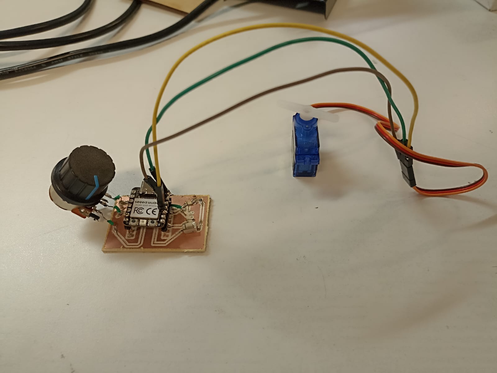
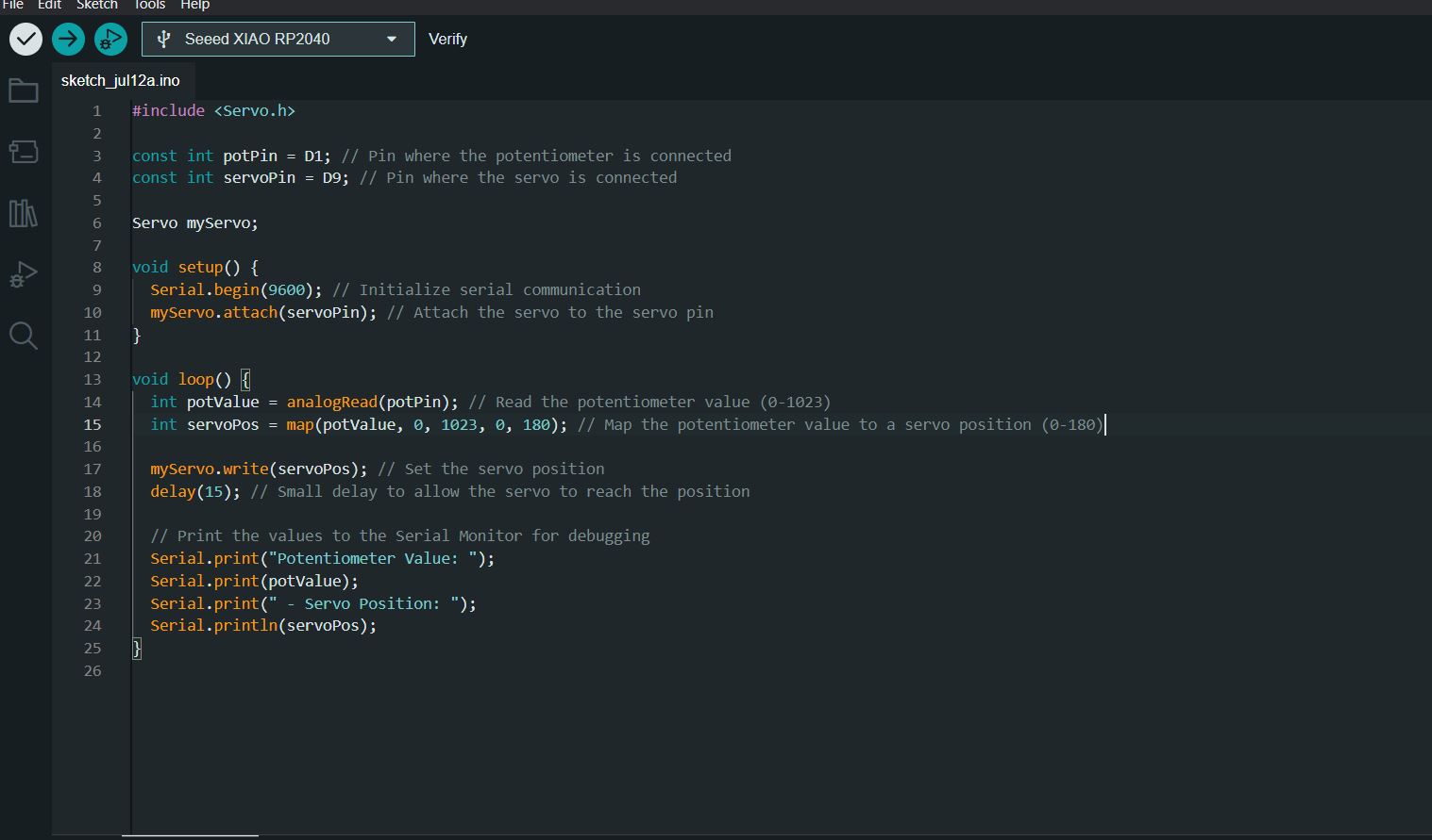
The code is a verys simple analog read on the potentiomter pin, and then using the map function to translate the value of the potentiometer to a value for the servo between 0° and 180°. The serial print is just to see both values on the console.
And here´s the PCB functioning:
Conclusions:
Creating a PCB from a copper laminate using a CNC machine was a very effective way to quickly create a board. I previously had done boards using ferric acid. A process that takes too long, it´s very tedious, pollutes a lot and has very mixed results. This way of creating PCBs offers a very practical alternative to prototyping with different boards and configurations for specific projects. I also learned how to design using EasyEDA and how to add basic components to your boards. Lastly, I learned how to set up and cut copper laminates using thee monoFab Roland, and how to solve problems that came along with the machine.