8. Electronics Design
Let's start with the basics:
Voltage is like the push or power that makes electricity move through things like wires. Imagine it's like the force that pushes a ball down a slide - the higher the slide, the faster and stronger the ball moves. Voltage is what makes electricity flow and do things like turn on lights or make machines work
Current is like the flow of water in a river. It's the movement of electricity through wires or circuits. Just like how water flows in a river, electricity flows in a circuit to power things like lights and toys. So, current is what makes electricity move and do things.
Power is like the strength or ability of something to do work or make things happen. For example, when you press a button and a toy moves, that's because it has power. Power can also make lights turn on or machines do their jobs. It's what gives things the energy they need to work.
Ohm's law
Ohm's Law is a fundamental principle in electronics that relates the voltage, current, and resistance in an electrical circuit. It is expressed mathematically as:
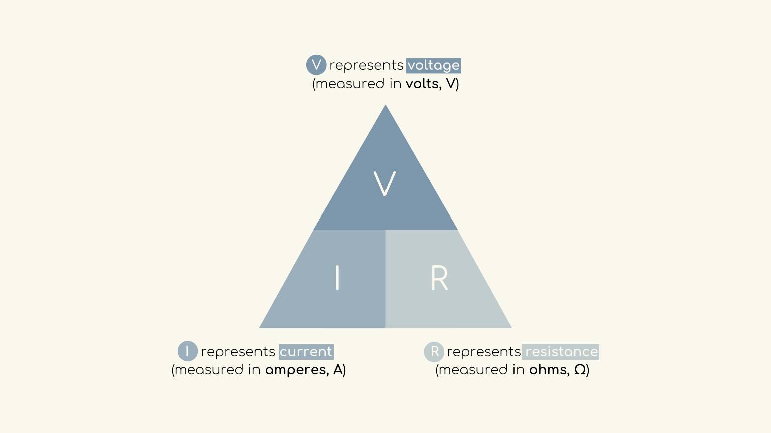
Ohm's Law is crucial in electronic design for analyzing and designing circuits. It enables engineers and designers to calculate and predict the behavior of electrical components and circuits. For instance:
- Calculating Voltage: If you know the current flowing through a circuit and the resistance of the components, you can use Ohm's Law to calculate the voltage across those components
- Calculating Current: If you know the voltage applied to a circuit and the resistance, you can determine the current flowing through the circuit.
- Calculating Resistance: If you know the voltage across a component and the current flowing through it, you can find the resistance of that component.
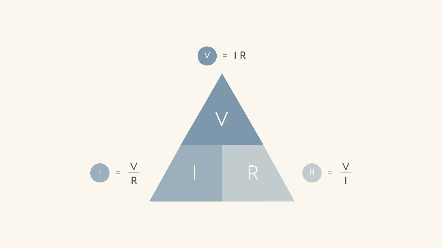
In resume, engineers can design and troubleshoot electronic circuits effectively by understanding and applying Ohm's Law. This ensures that the components operate within safe and desired parameters.
Basic Components
| Component | Symbol | Description | Notes |
| LED | 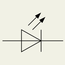 |
A LED (Light-Emitting Diode) is a type of semiconductor device that emits light when an electric current passes through it. |
|
| Button | 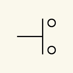 |
Refers to a physical or electronic component used to control or trigger specific actions within an electrical or electronic system. |
|
| Trainer |  |
A device or system designed to facilitate learning, experimentation, and practical hands-on experience with electronic circuits, components, and concepts. |
|
| Resistance |  |
Property of a material or component that opposes the flow of electrical current. It is denoted by the symbol R and is measured in ohms (Ω). |
|
Electronics Design Softwares
Altium
Altium Designer, is an electronic design automation (EDA) suite of tools used for designing integrated circuits (ICs), printed circuit boards (PCBs), and field-programmable gate arrays (FPGAs). For schematic capture, PCB layout, component management, signal integrity analysis, and design collaboration, Altium Designer provides an extensive toolkit.
It has:
- Unified Design Environment: By offering a single platform for PCB layout, design verification, and schematic capture, it streamlines the design process and minimizes the need to transition between different software products.
- Simple User Interface: The program has a straightforward user interface that is easy to use, so both inexperienced and seasoned users can utilize it.
- Advanced Features for PCB Design: Altium Designer provides a plethora of advanced features for PCB design, such as support for multi-board design projects, interactive routing, high-speed design tools, and 3D visualization.
- Steep Learning Curve: Although it has an intuitive user interface, it can take some time for novice users to become proficient with all of its features and capabilities.
- System Requirements: Because Altium is a resource-intensive program, it can need a powerful computer to function well, especially when handling intricate designs or sizable PCB layouts.
- Restricted Compatibility: Altium Designer can import and export designs in a variety of file formats, but it might not be completely compatible with other EDA software tools. This could present difficulties when working with designers who utilize different software platforms.
Eagle
Eagle is a electronic design automation (EDA) program that provides auto-routing, PCB layout, schematic capture, and extensive library content. It can be acquired via Autodesk Fusion, a comprehensive solution for product development that combines design, simulation, electronics, manufacturing, and teamwork.
Some of its characteristics are:
- User-Friendly Interface: Eagle streamlines the design process with tools like schematic capture and a PCB layout editor, making it appropriate for both inexperienced and seasoned PCB designers.
- Huge Component Library: Eagle offers a vast collection of electronic parts, footprints, and symbols from different manufacturers, which minimizes manual search work and boosts efficiency.
- Community Support and Resources: Eagle has a vibrant user base that provides online resources, tutorials, and support forums to help with learning and skill development. Its functionality is increased through integration with external tools.
- Limited Flexibility: In comparison to other PCB design tools, Eagle may lack some parts or features required for specialized applications, and customization choices may be restricted. This limits Eagle's ability to create customized designs.
- Learning Curve: Eagle is a sophisticated program that can take a lot of time and effort to master, especially for new users or those working with intricate circuit designs. The lack of detailed coverage of certain topics in the software's documentation and tutorials may present additional difficulties for novice users.
Easy EDA
Easy EDA is a program where can be designed electronic circuits, printed circuit boards, and schematics. It offers an easy-to-use interface for designing and altering circuit designs, making it available to enthusiasts, learners, and experts in the electronics industry. EasyEDA is a complete electronic design project solution with capabilities including schematic capture, PCB layout, simulation, and collaboration tools.
- Ease of Use: Is renowned for having an intuitive design and user-friendly interface. It makes electronic circuit design easier to understand and more manageable for both novice and seasoned engineers. Its simplicity of use is enhanced by the wide component libraries, interactive tools, and drag-and-drop functionality.
- Cloud-Based Collaboration: EasyEDA, a cloud-based platform, enables several users to collaborate on a single project at once. Version control and real-time updates make sure that everyone is in agreement.
- Tool Integration: EasyEDA streamlines the entire electronic design process by combining many design tools into a single platform. Users don't need to export/import files across several software programs in order to move from schematic capture to PCB layout and circuit simulation.
- Limited Offline Functionality: Users must have an internet connection because it is a cloud-based platform. This dependence on internet connectivity may provide a challenge, particularly in settings lacking reliable internet access.
- Dependency on Third-Party Libraries: EasyEDA comes with a number of built-in component libraries, however users could run across circumstances where some models or components they need aren't accessible. Users are forced to use third-party libraries or make their own bespoke components in these situations, which can be time-consuming and lead to compatibility problems.
KiCad
Kicad is an open-source electronic design automation (EDA) software package, is used to design printed circuit boards (PCBs) and create schematics. It provides a full toolkit for routing, PCB layout, and schematic capture.
It’s characteristics are:
- Schematic Capture: Using a graphical interface, users can place, connect, and annotate components inside the schematic editor to produce electronic schematics.
- PCB Layout: By allowing users to place components, specify footprints, and arrange them as needed, KiCad simplifies the construction of physical PCB layouts.
- Footprint Editor: Users can specify the physical arrangement and measurements of every component on the PCB by using tools for creating and changing component footprints.
- CB Routing: KiCad offers tools for establishing appropriate connectivity and signal between PCB components by routing traces.
- 3D Viewer: KiCad comes with an integrated 3D viewer that lets users see PCB designs in three dimensions
Group Assignment
Visit our group task by clicking on the button below.
What did I do this week?
This week, I wanted to design my PCB in relation to some aspects of my final project. So I designed my PCB based on the combination of colors, with each basic geometric figure representing a primary color. To better understand this concept, I created a diagram.
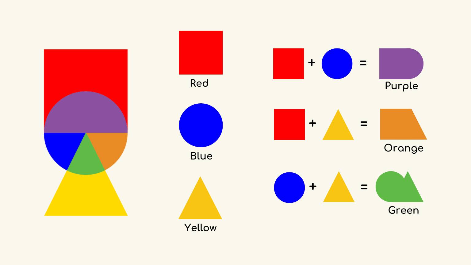
I used Neopixels to achieve these color combinations in the specific parts where the figures intersect, as shown in the diagram. In the following paragraphs, I will explain how I developed this idea.
starting design!
Prior to designing my board, I compiled a list of the components that I would utilize in order to facilitate their incorporation into the design process.
- 1 LED
- 1 Capacitor
- 1 Resistor (1001)
- 1 Button
- 1 Resistor (1002)
- 6 Neopixels
- 8 Pines
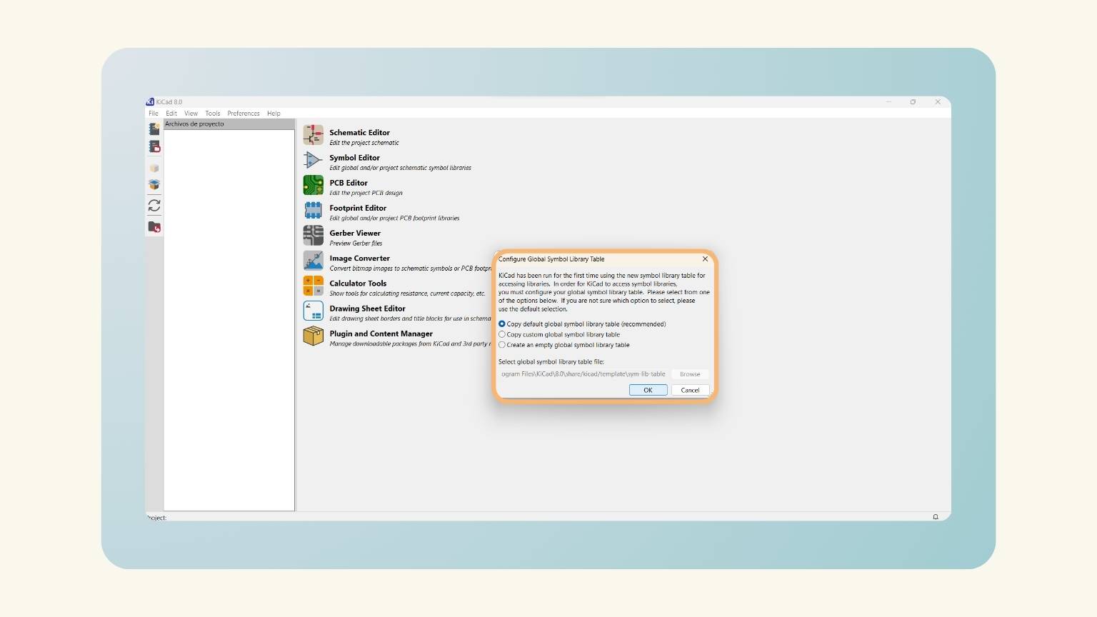
Subsequently, I proceeded to design the board in KiCad, adhering to the following procedure:
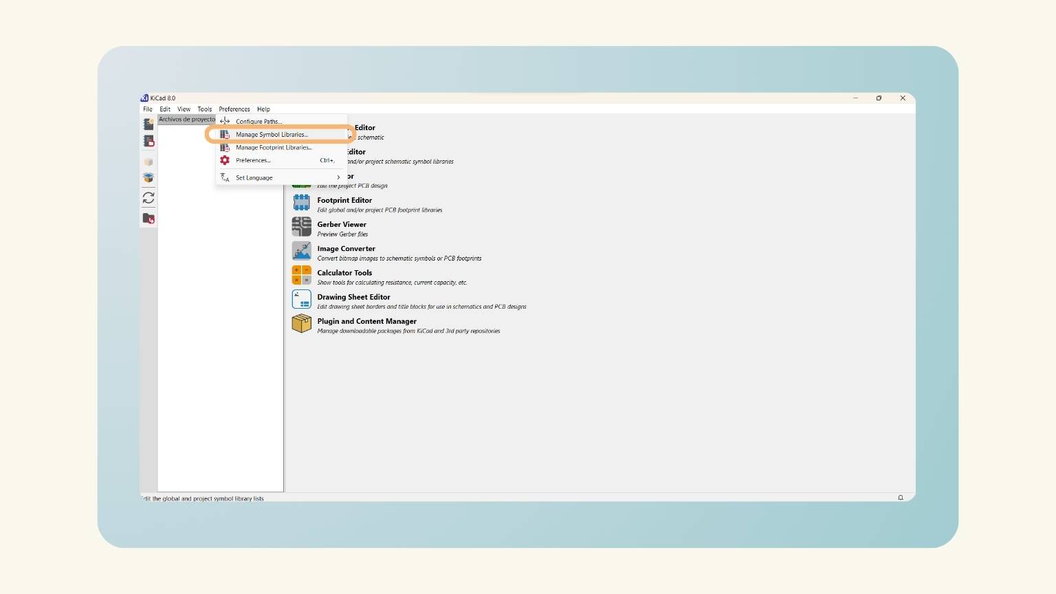
- First, I opened ‘KitCad’ software.
- To integrate these libraries, I selected the ‘’Preferences’ menu, then clicked on ‘Manage Symbol Libraries...’ .
- And add appeared, and I pressed ‘OK’ .
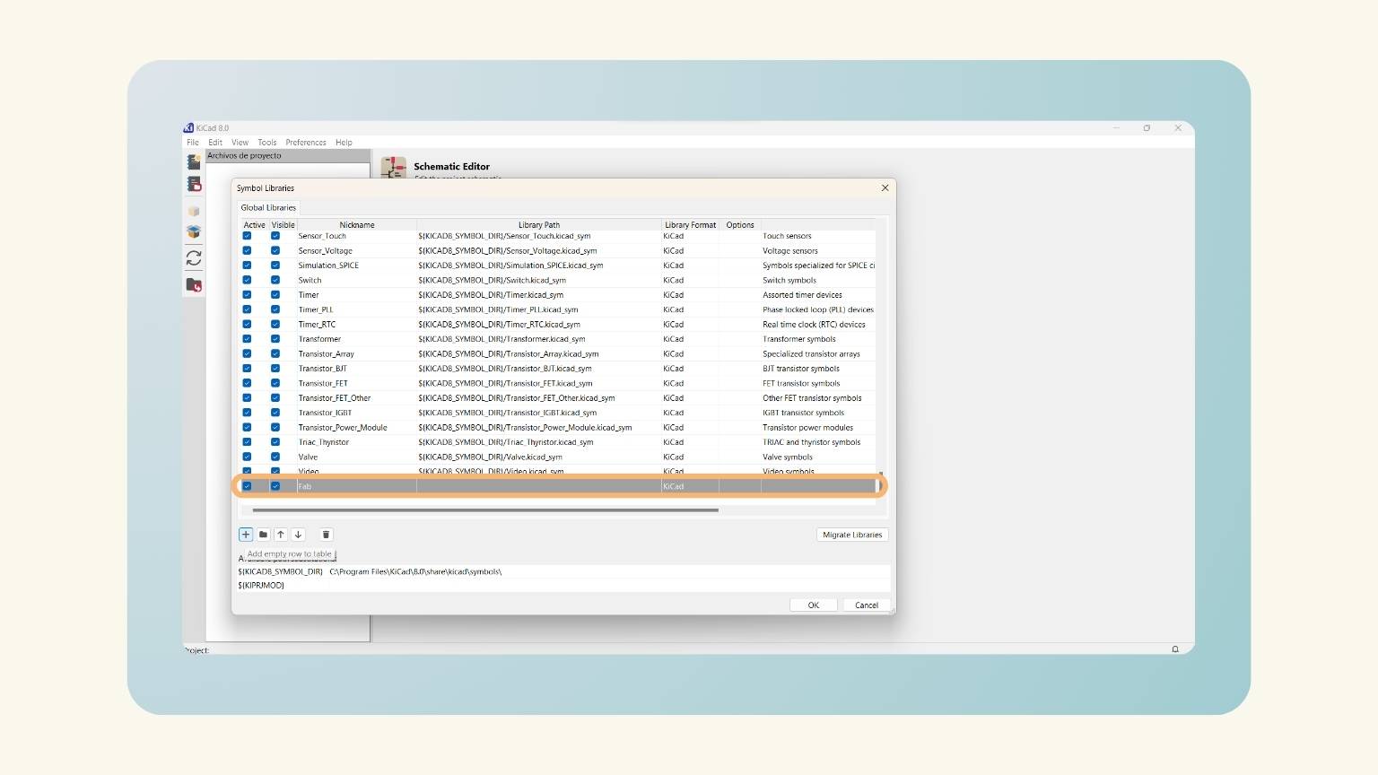
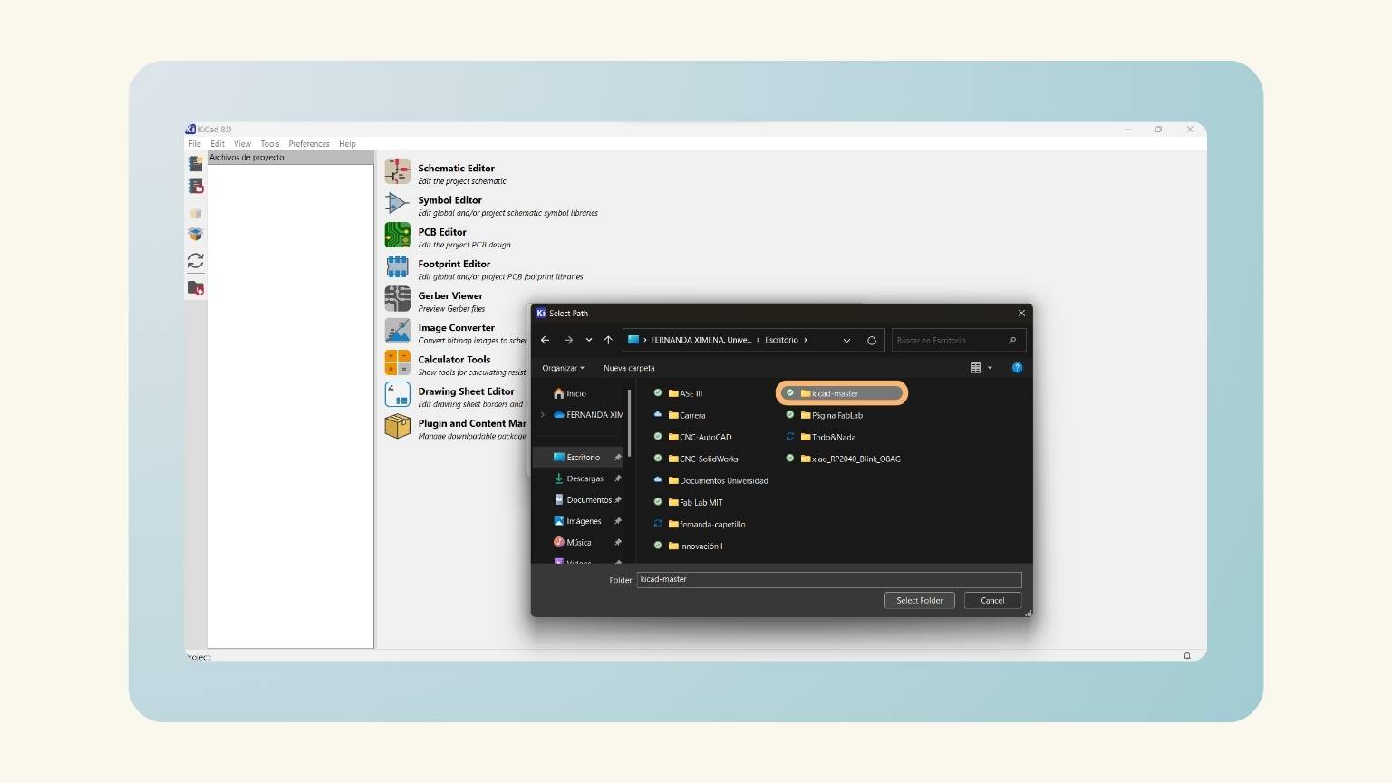
- I created a new ‘Library Path’ called ‘Fab’ .
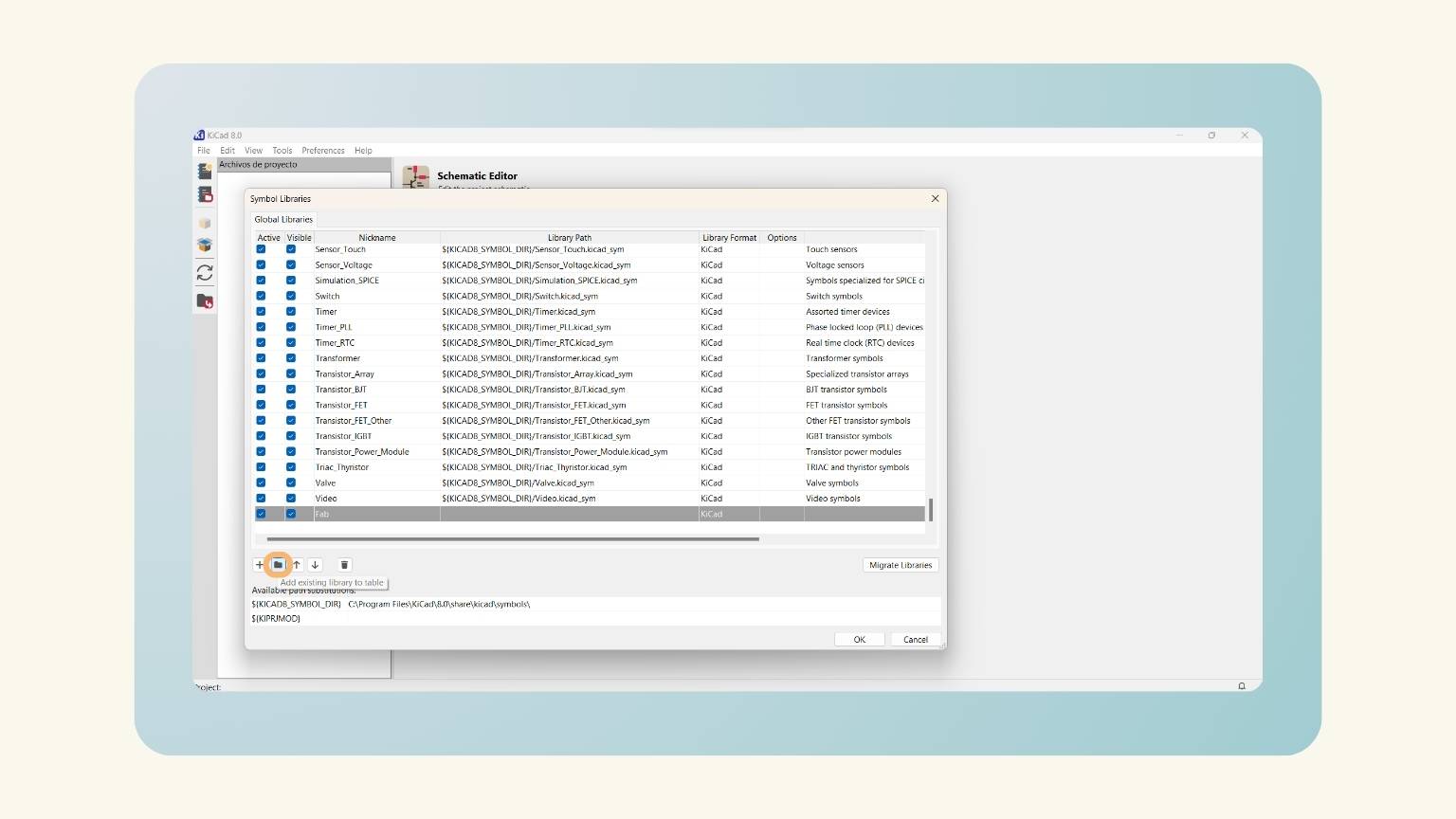
- I added an existing library. For this, I clicked on the folder icon.
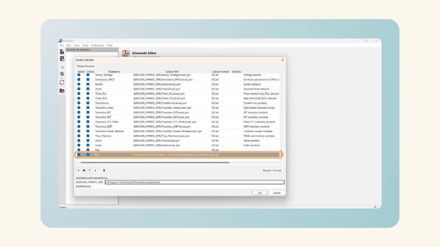
- In this case, I included the ‘fab.pretty file.
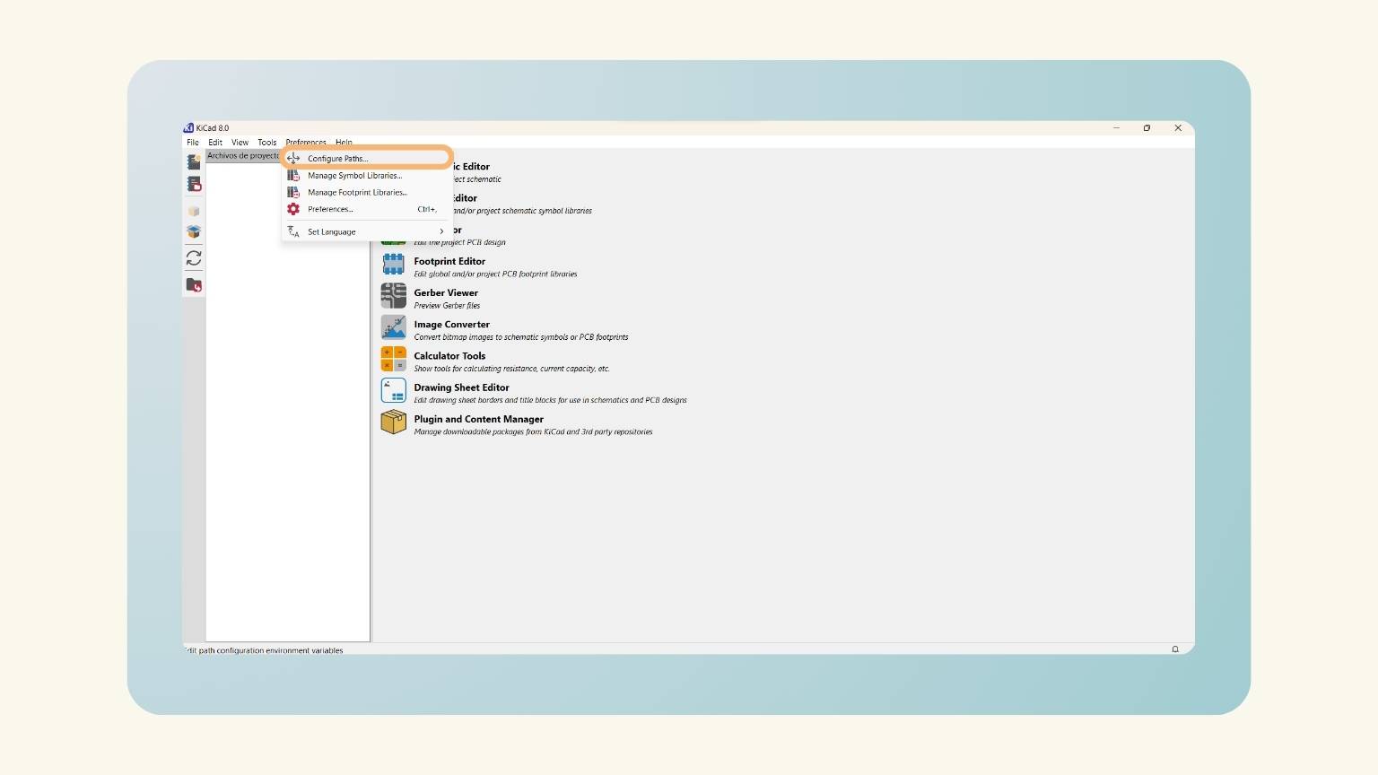
- I returned to the start menu, opened the ‘’Preferences’ menu, and clicked on ‘Configure Paths...’.
- I added the ‘fab.kitcad_sym’ file.
- And I have the library installed.
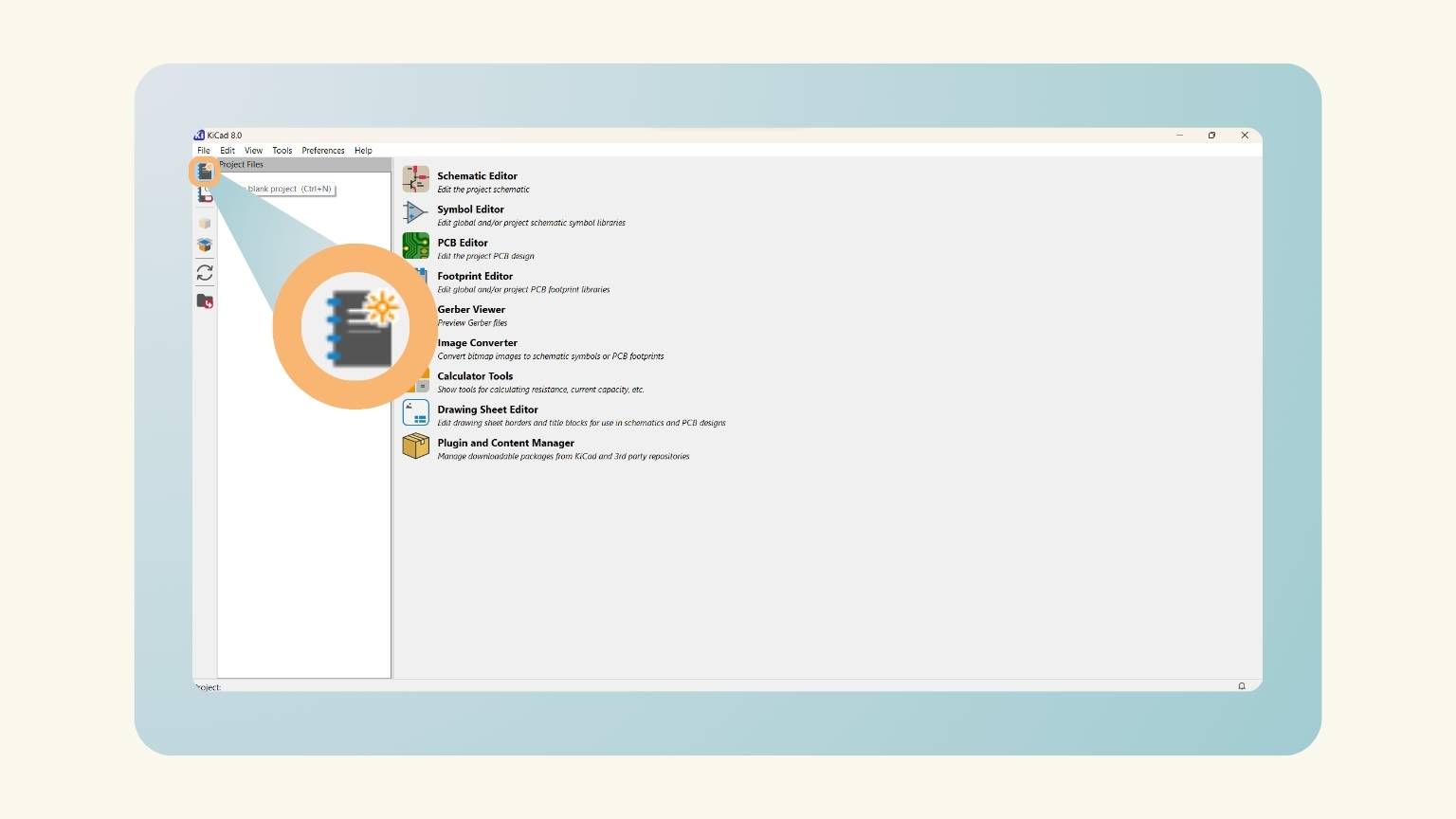
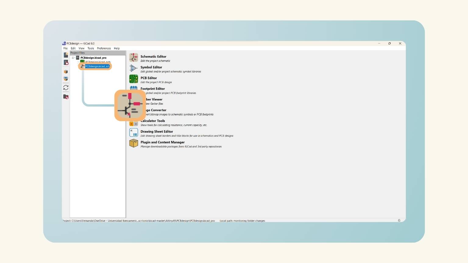
- I selected the first option of the lateral menu, ‘Create a new blank project’.
- I named the project, and it appeared in the 'Project Files' section.
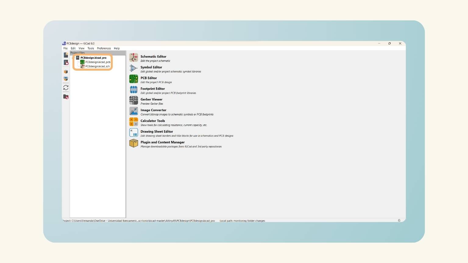
- Then I opened the ‘Schematic Editor’ by clicking on the document 'PCBdesign.kitcad_sch’.
- The ‘Schematic Editor’ was open.
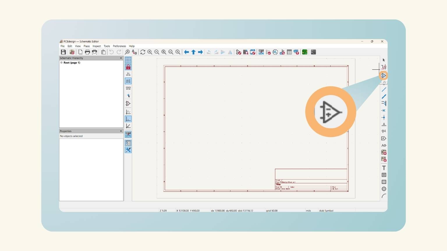
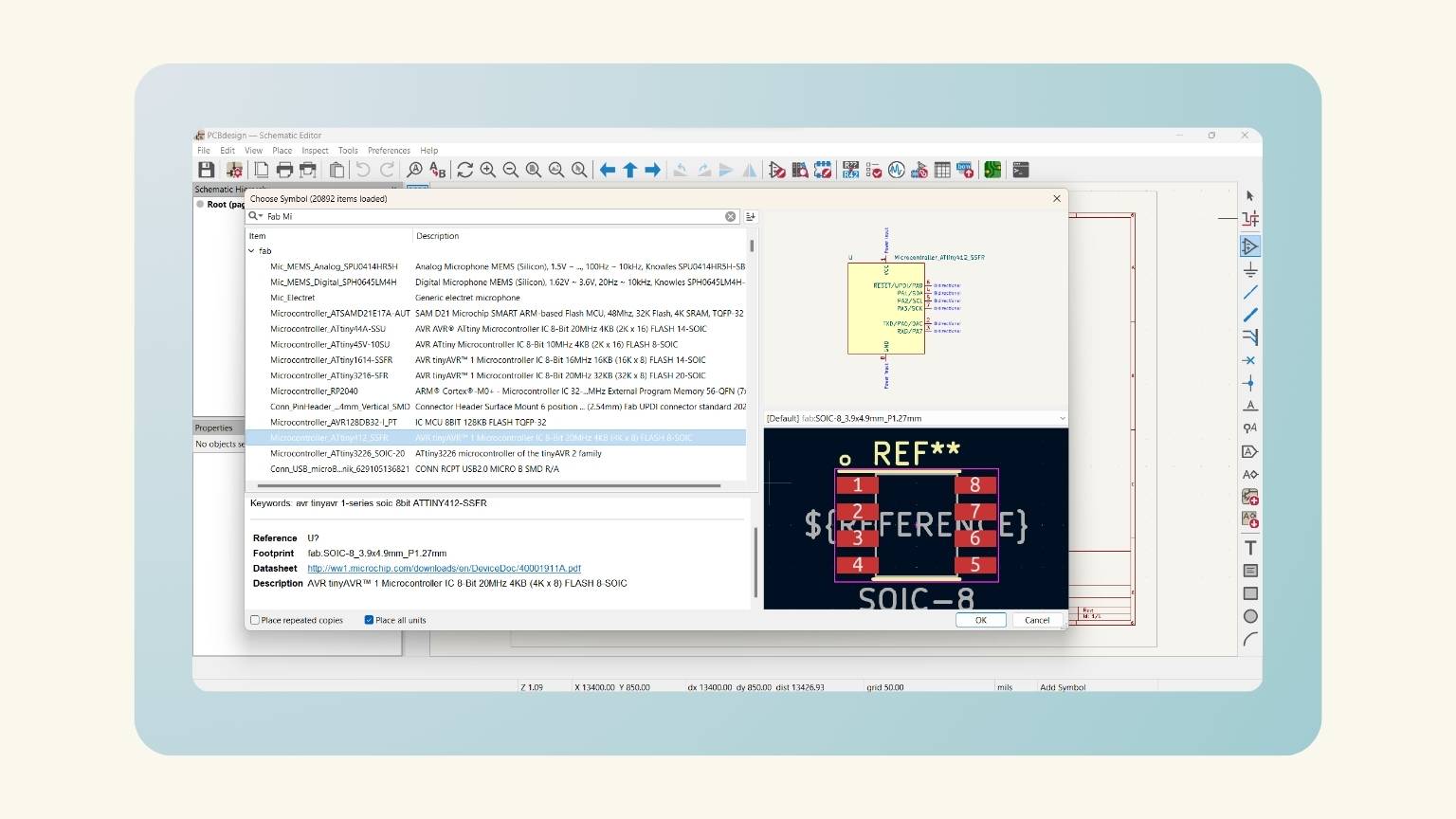
- I selected the third option in the right menu, ‘Add symbols’.
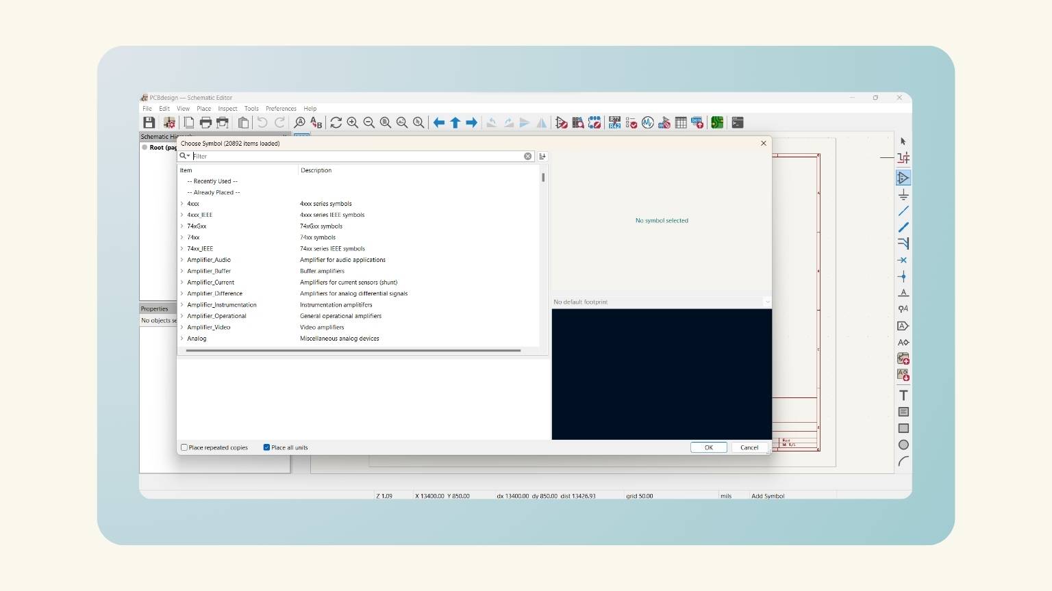
- The menu to find the symbol was open.
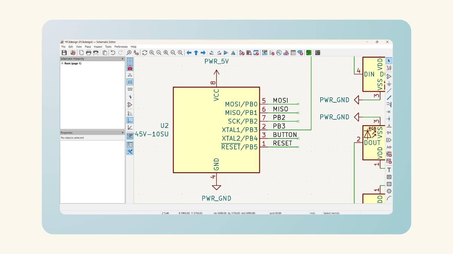
- I used the search bar to filter the symbol; to this end, I wrote‘Fab Microcontroller’ to find the component more easily
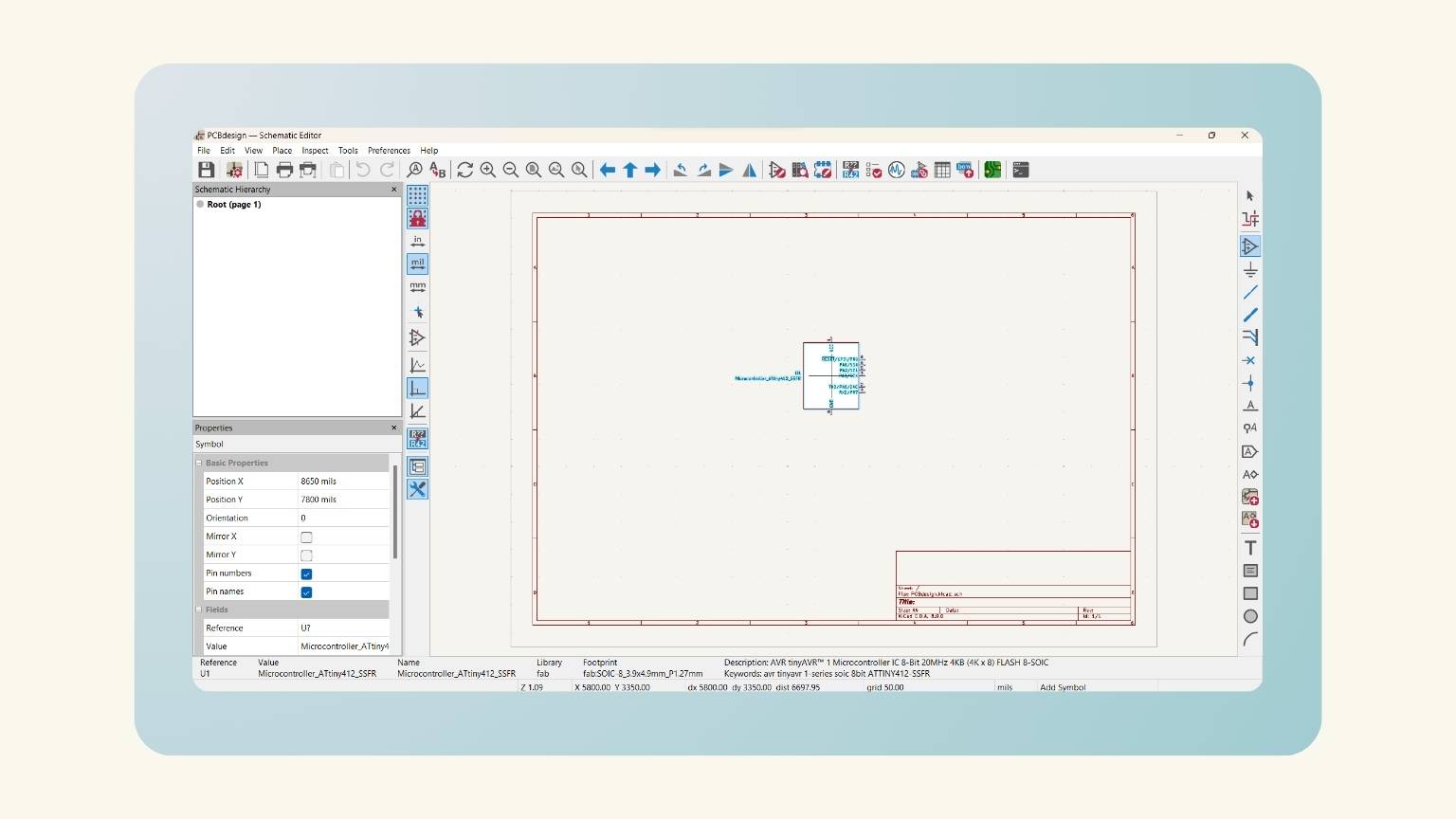
- I chose the microcontroller that I need. And I put the component on the page.
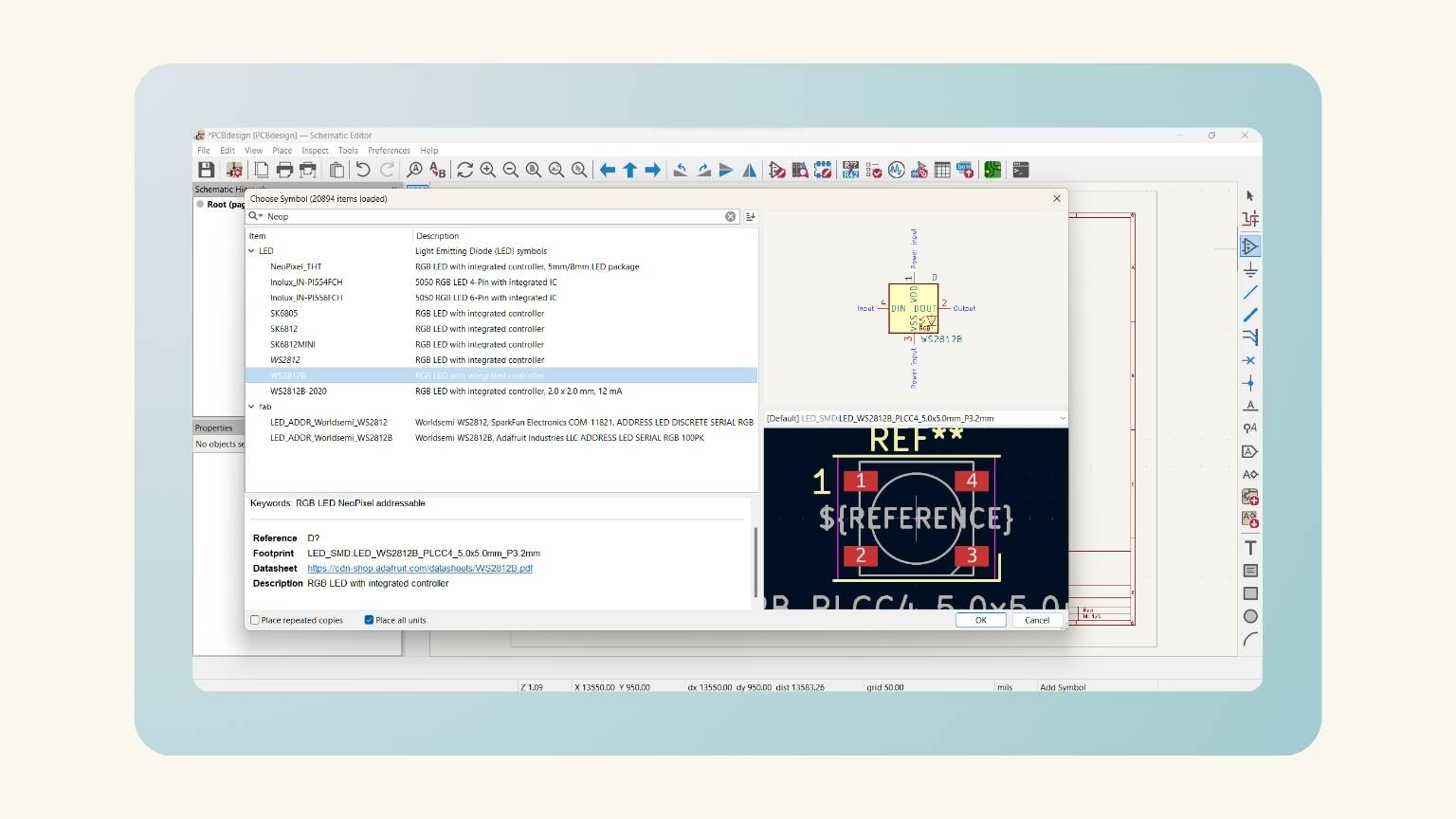
- I went again to the ‘Add symbols’ option to add the other components.
- Note: When you click on a component, you will see three things:
- In the lower box, you will find the measurements, main characteristics, and a link to see the data sheet.
- In the upper box on the right, you will see a preview of the schematic.
- And in the lower one, a preview of the PCB.
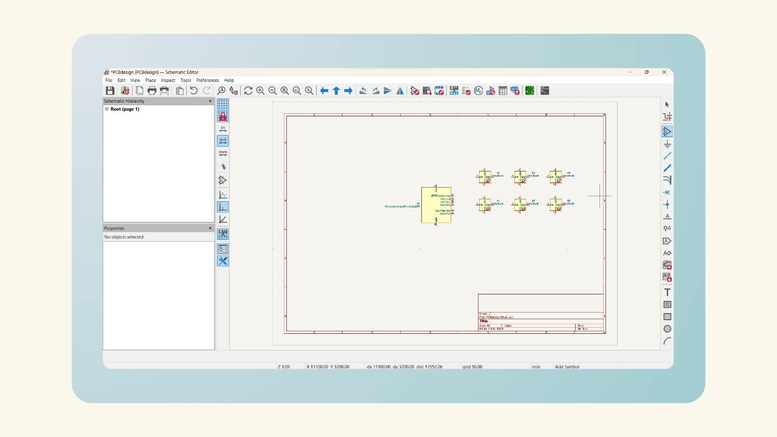
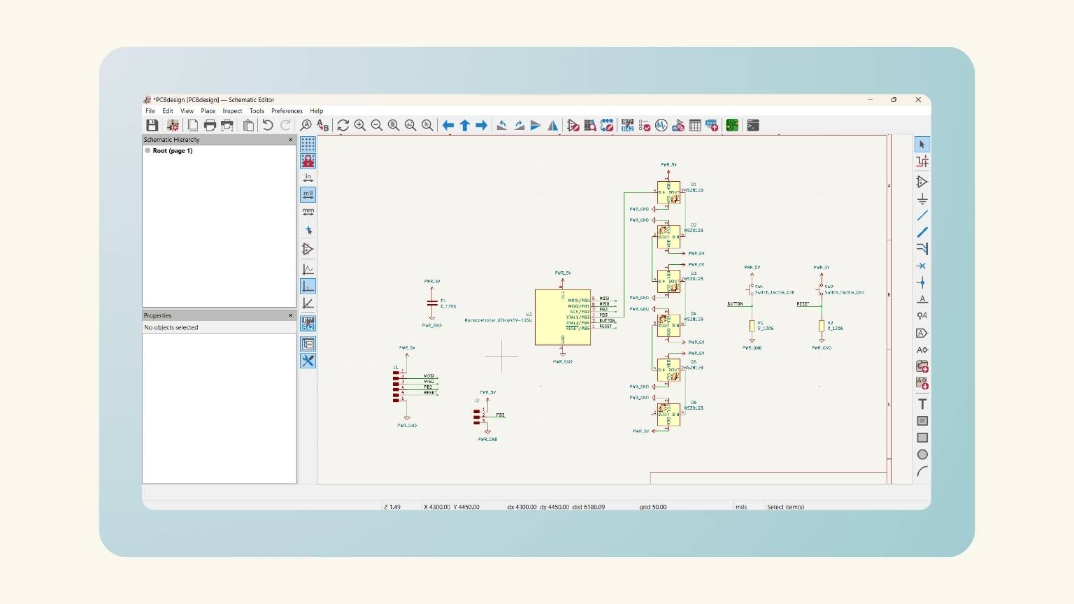
- I put in the schematic the components.
- Note: If you have already placed a component, you can simply copy and paste it into the schematic.
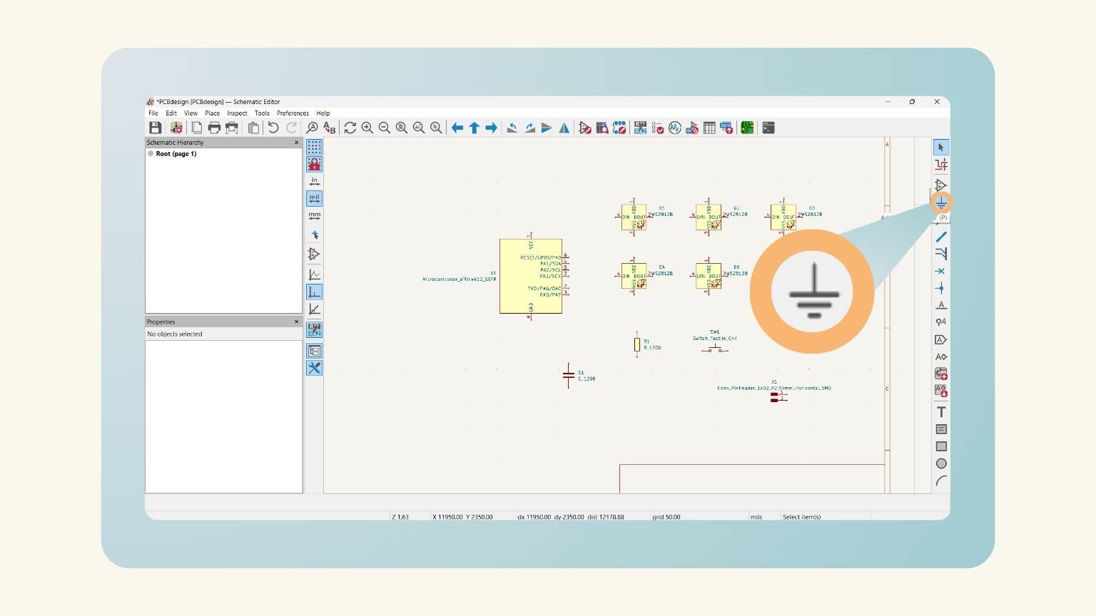
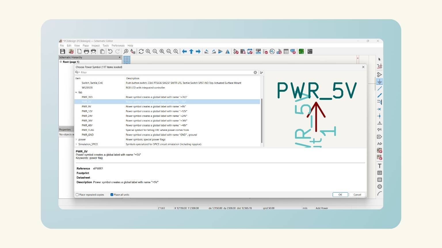
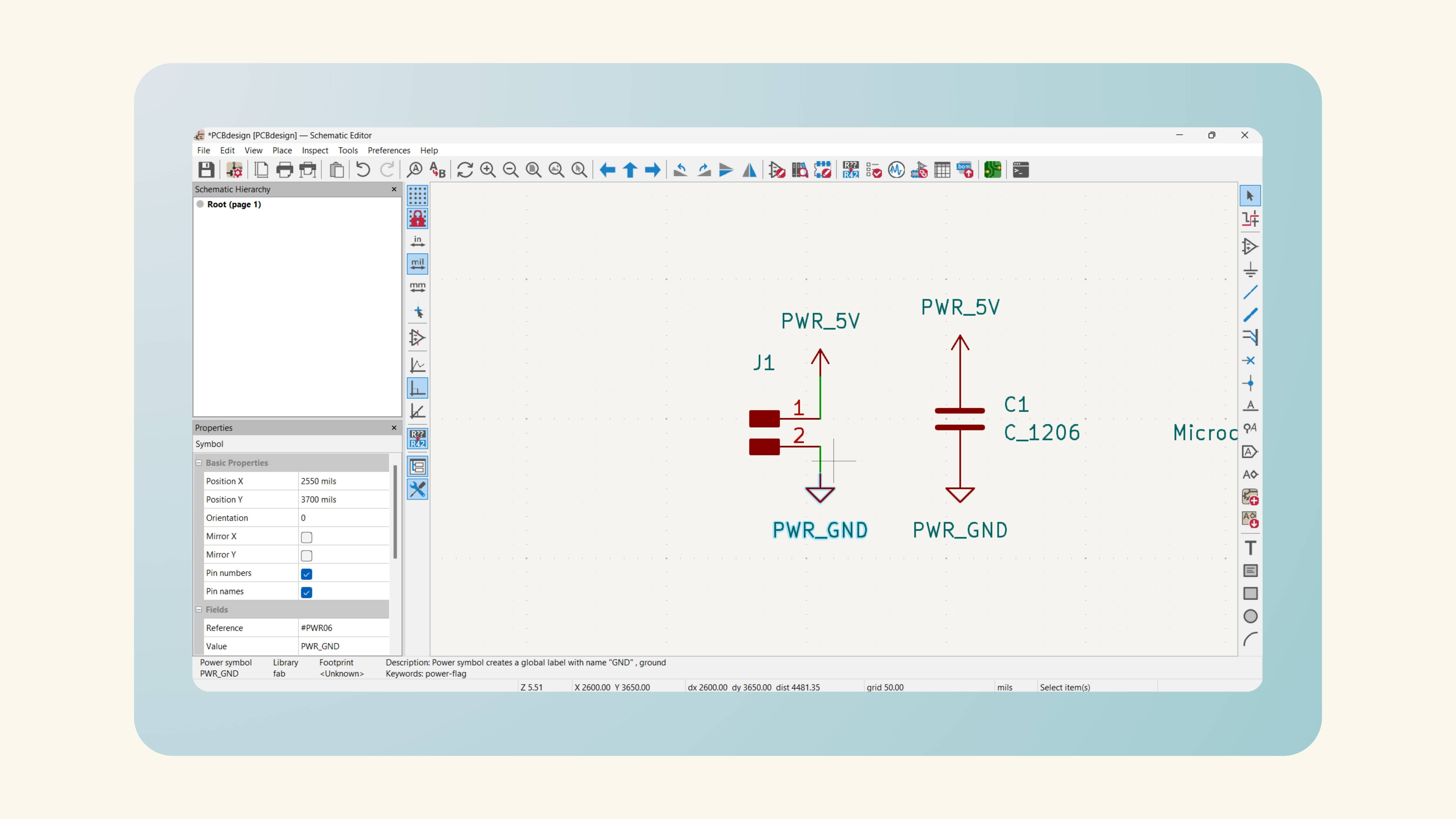
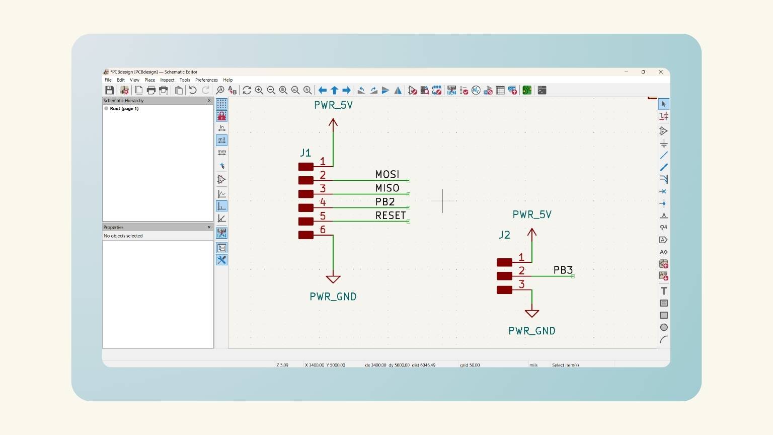
- I repeated the following steps to add the basic components to my PCB. Next, I selected the fourth option in the right menu, ‘Add power symbols’.
- The menu was open, and I selected ‘PWR_5V’.
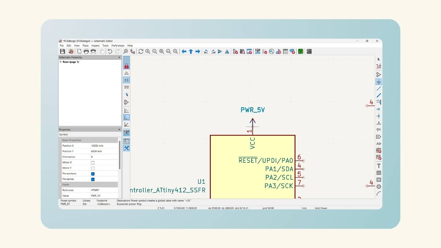
- Then, I put it in the VCC pin.
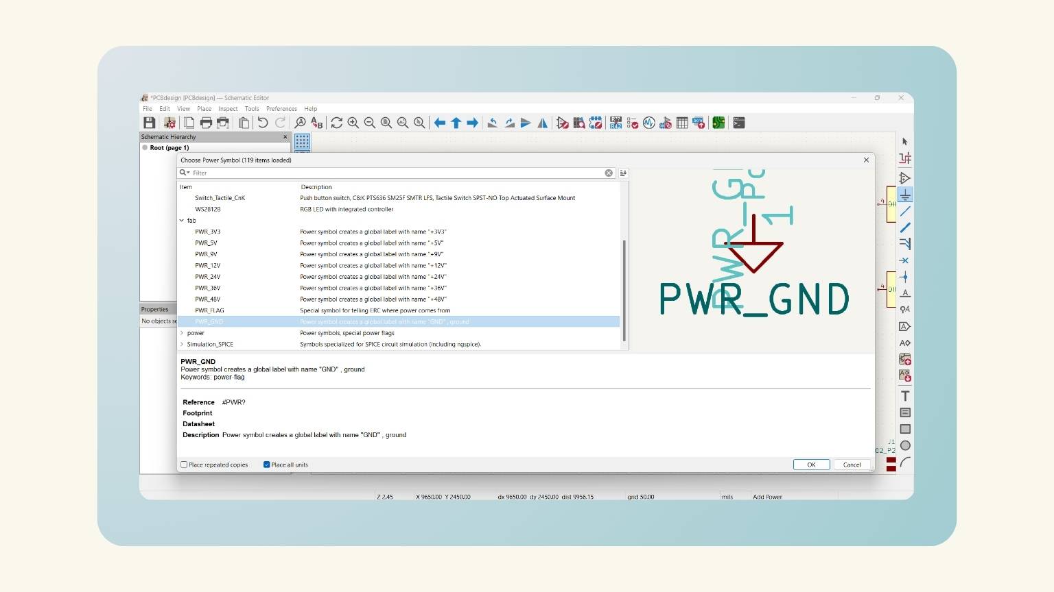
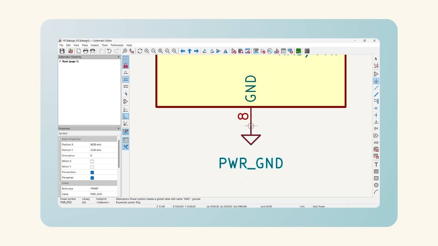
- I back to the ‘Add power symbols’ menu to put the ground.
- I put it in the GND pin.
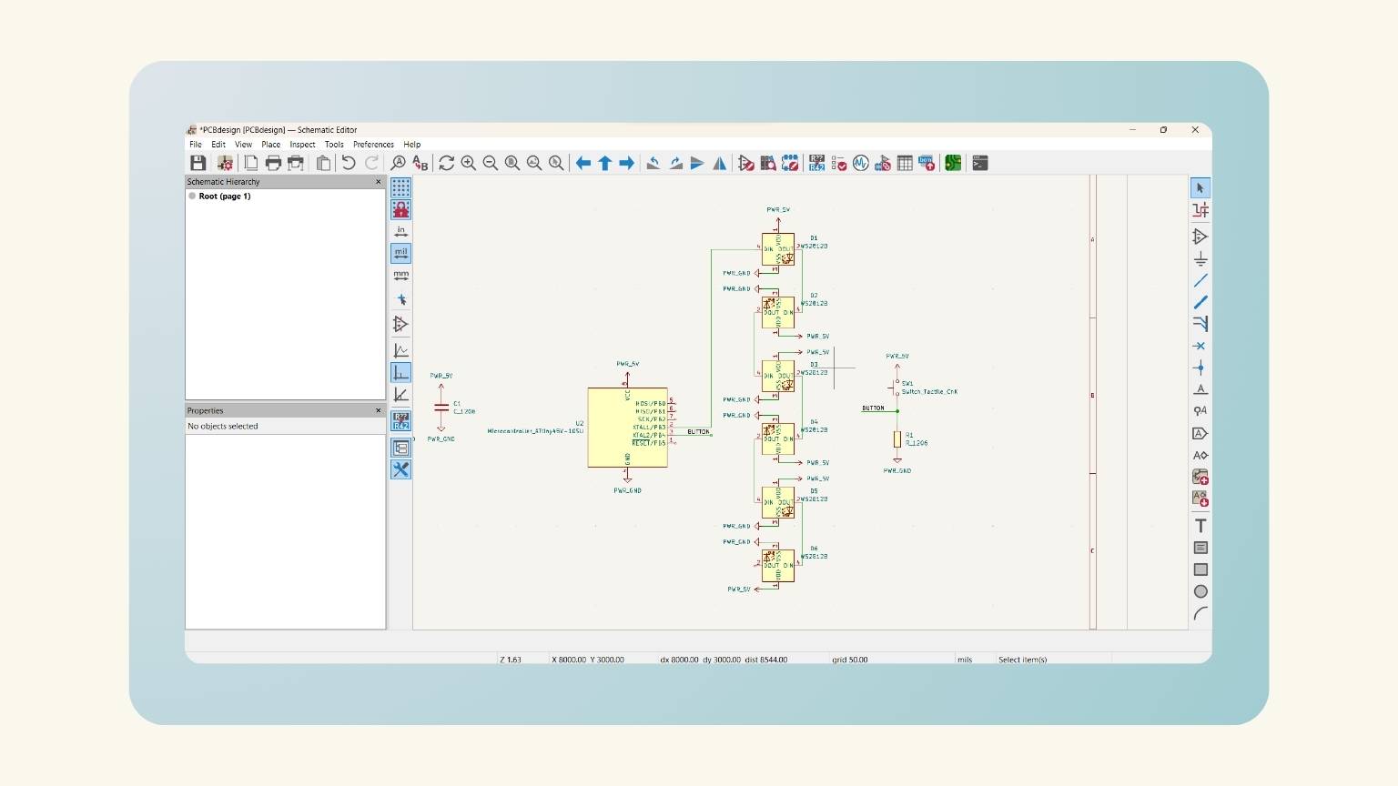
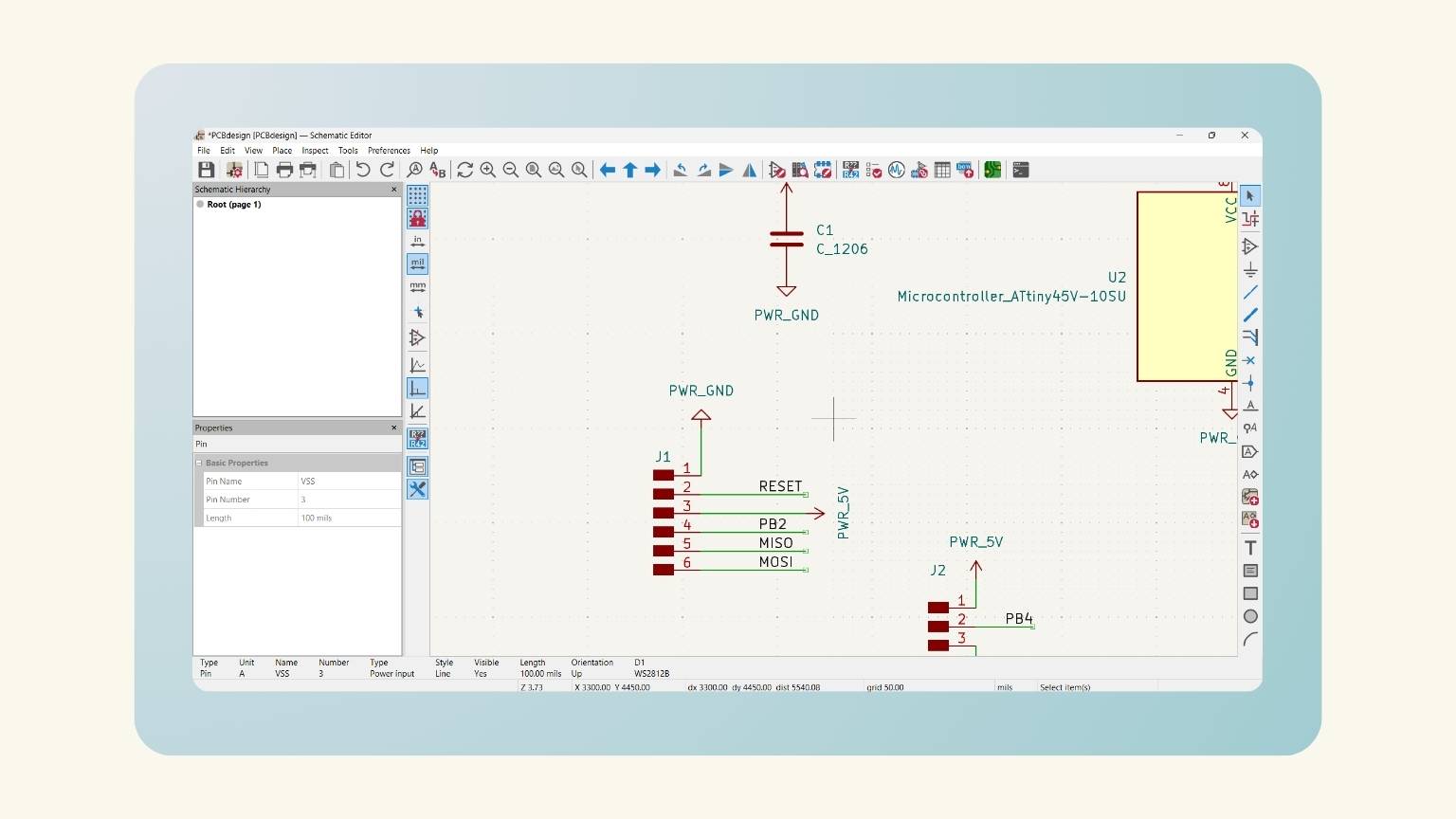
- Once the voltages and grounds had been placed on each component, I began to make the connections between them.
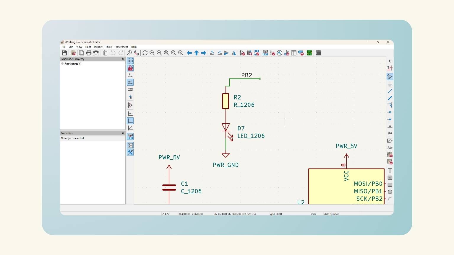
- I connected the Neopixels to the PB3 pin and the button to the PB4 pin
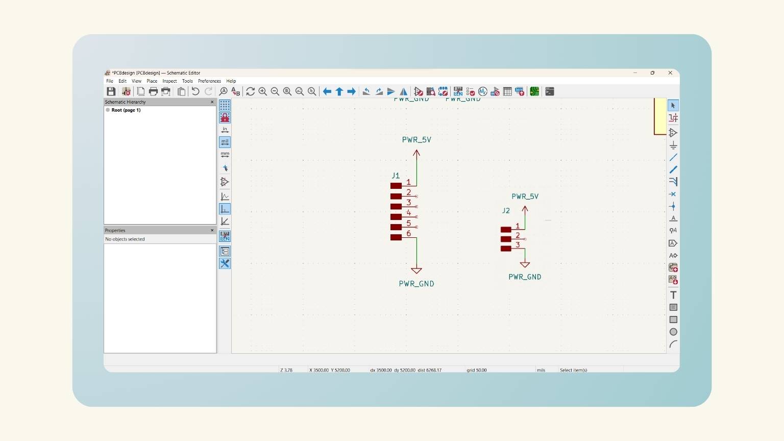
- After that, I added two sections of pins, one for five and the other for three.
- Then I realized the connections between the pins.
- In the microcontroller, I put the connections with ‘net labels’.
- Note: You can make a net label with the ‘Draw net labels’ option (the tenth option in the right menu).
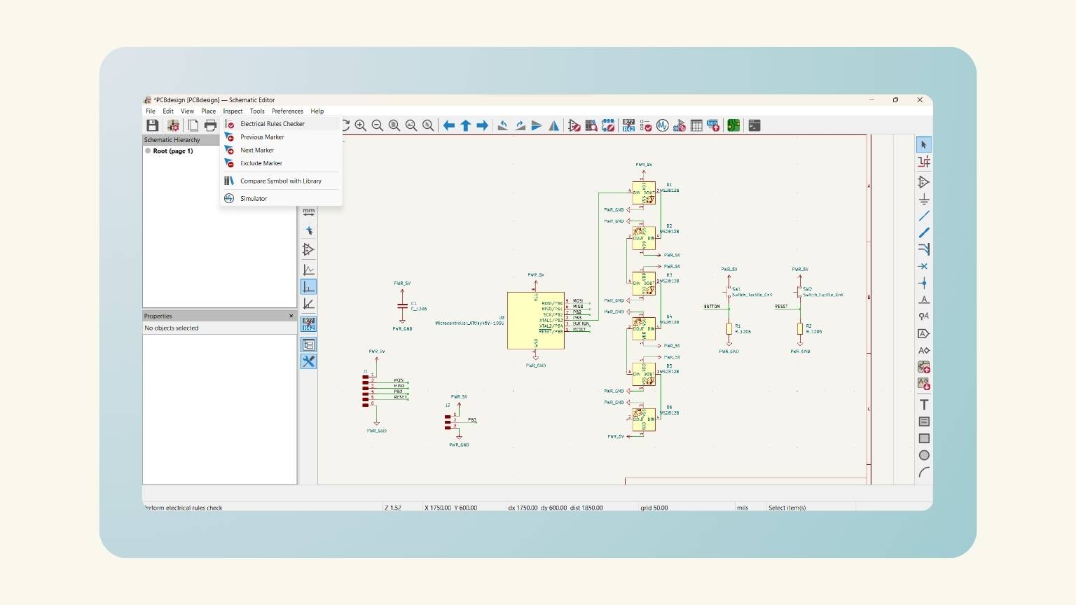
- And I finished my schematic!
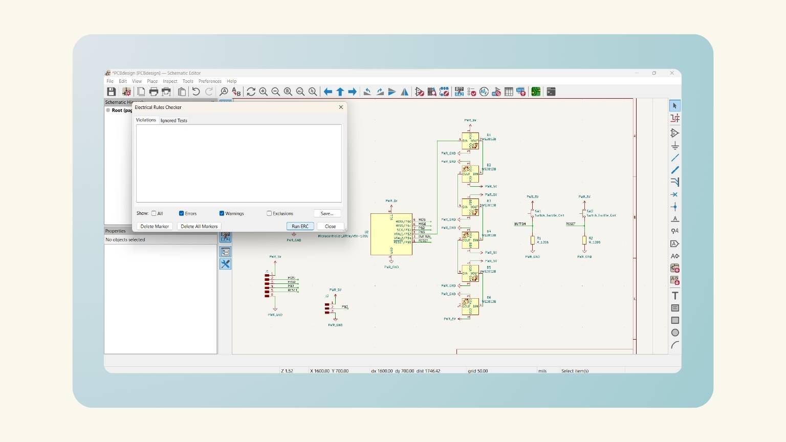
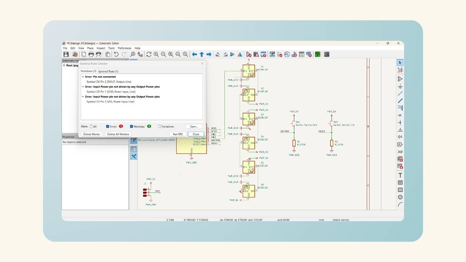
- To verify, I went to the ‘Inspect’ menu, specifically the ‘Electric Rules Checker’ option.
- A window opened, and I pressed the bottom next to close, ‘Run ERC’, to see the errors.
- And I visualized the errors to correct them and verify if everything was okay.
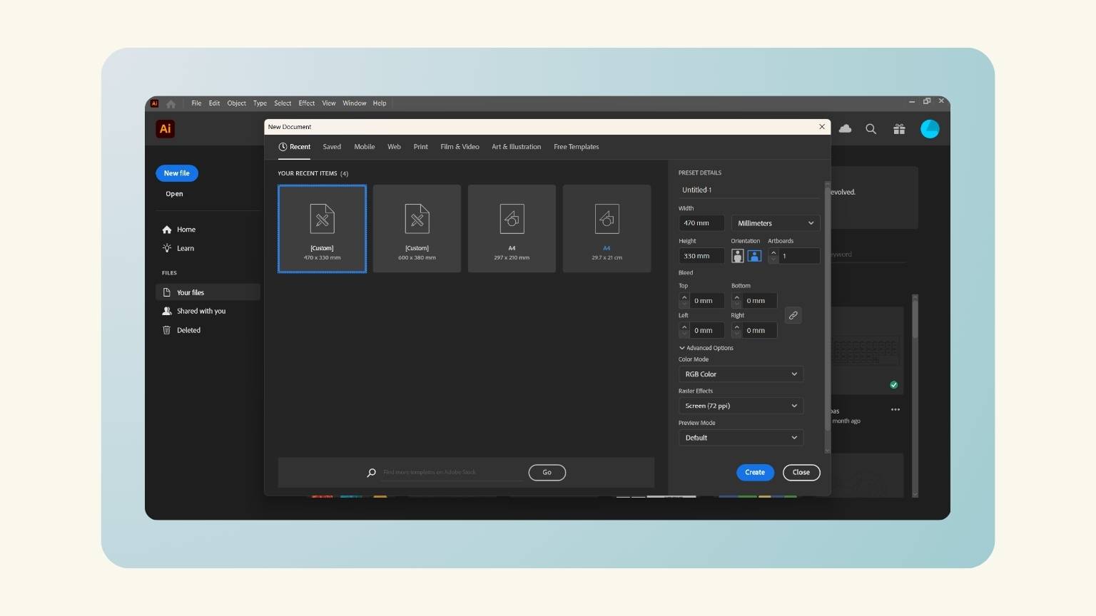
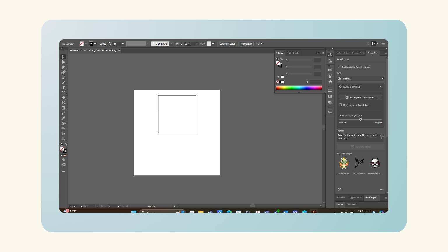
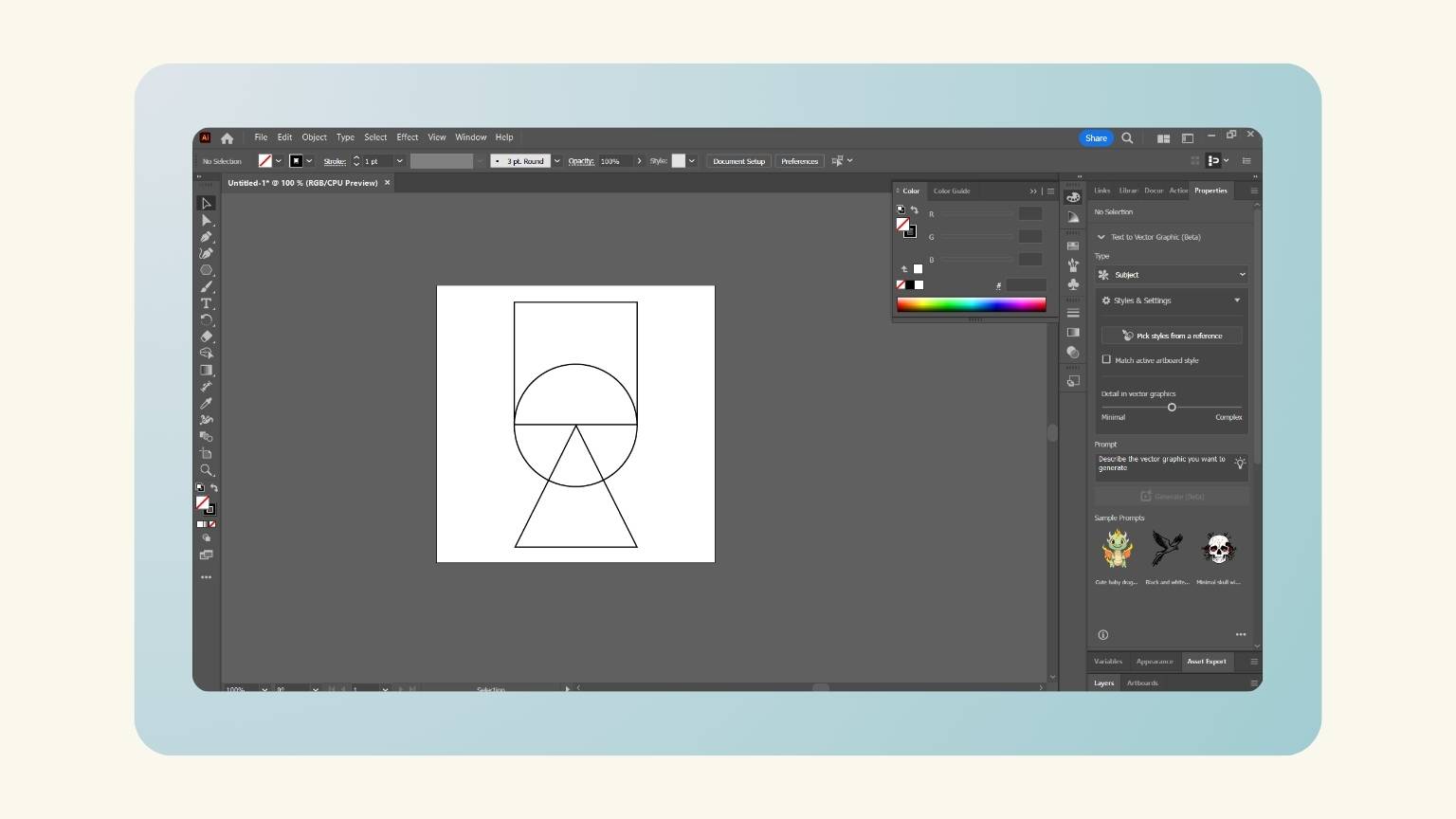
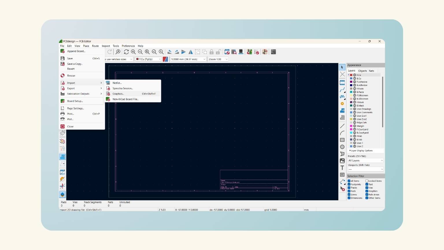
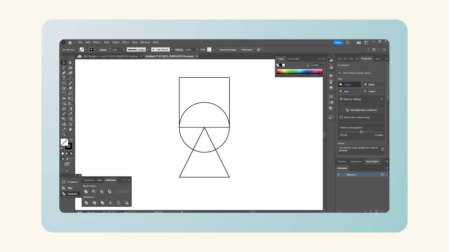
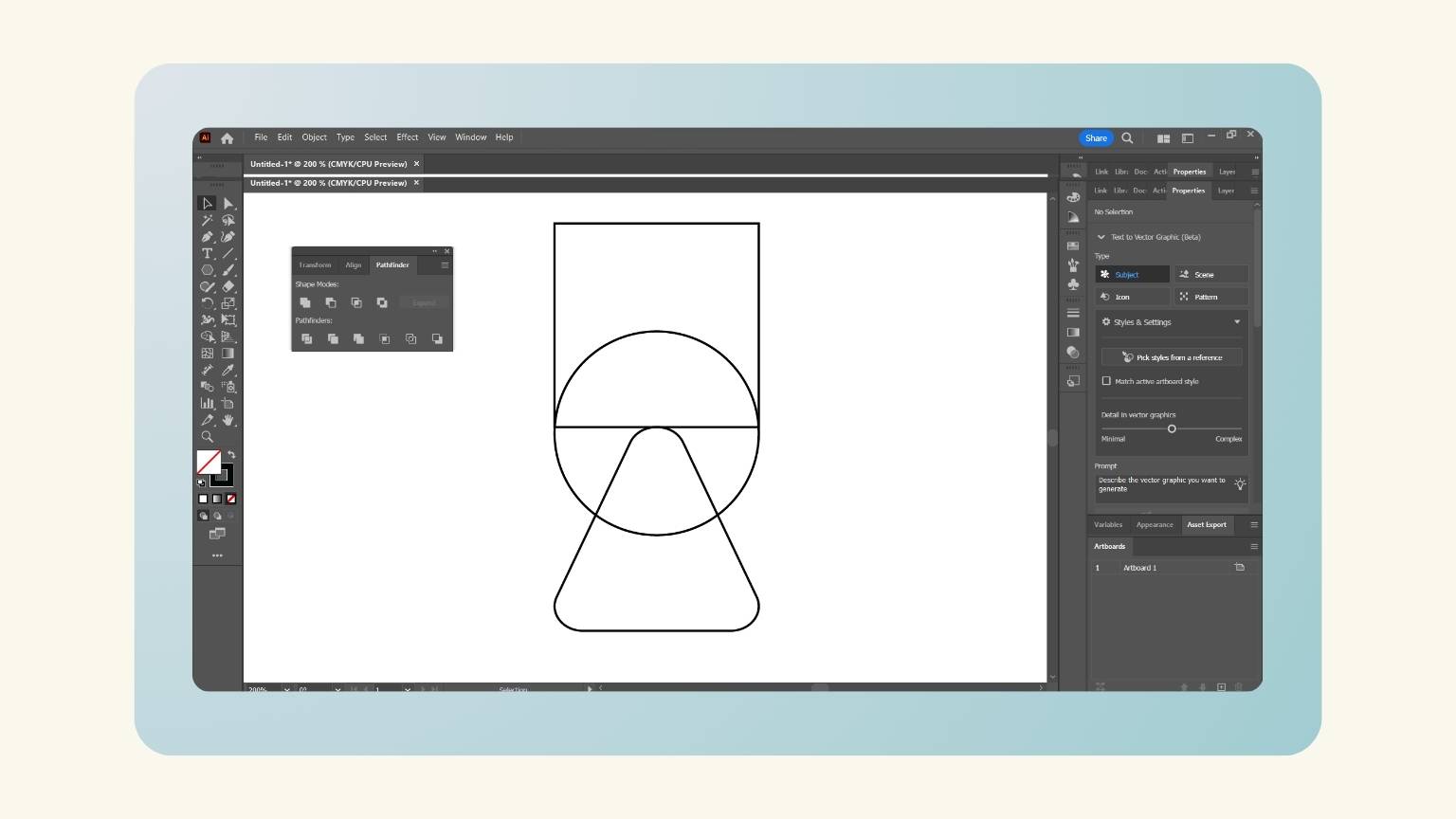
- I didn't want to make my PCB with a basic rectangular shape, so I used ‘Adobe Illustrator’ to make the shape I wanted.
- I created a new document.
- I started to create a square.
- Then, I made a circle and a triangle. And I accommodated one below the other.
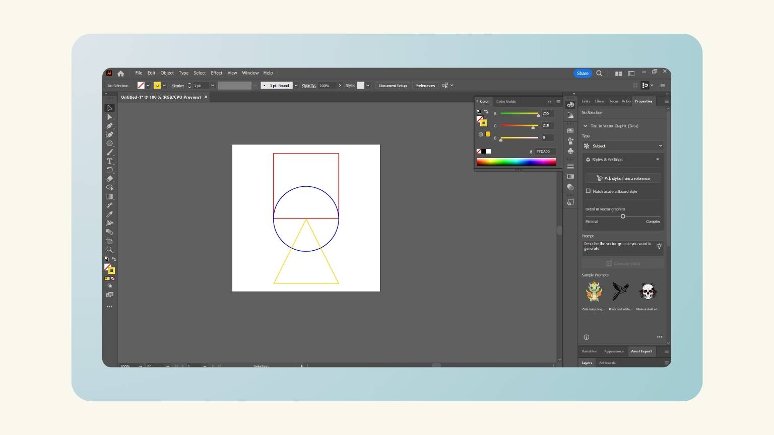
- I changed the colors of each figure, just to use it as a reference later.
- I saved the file as a dxf.
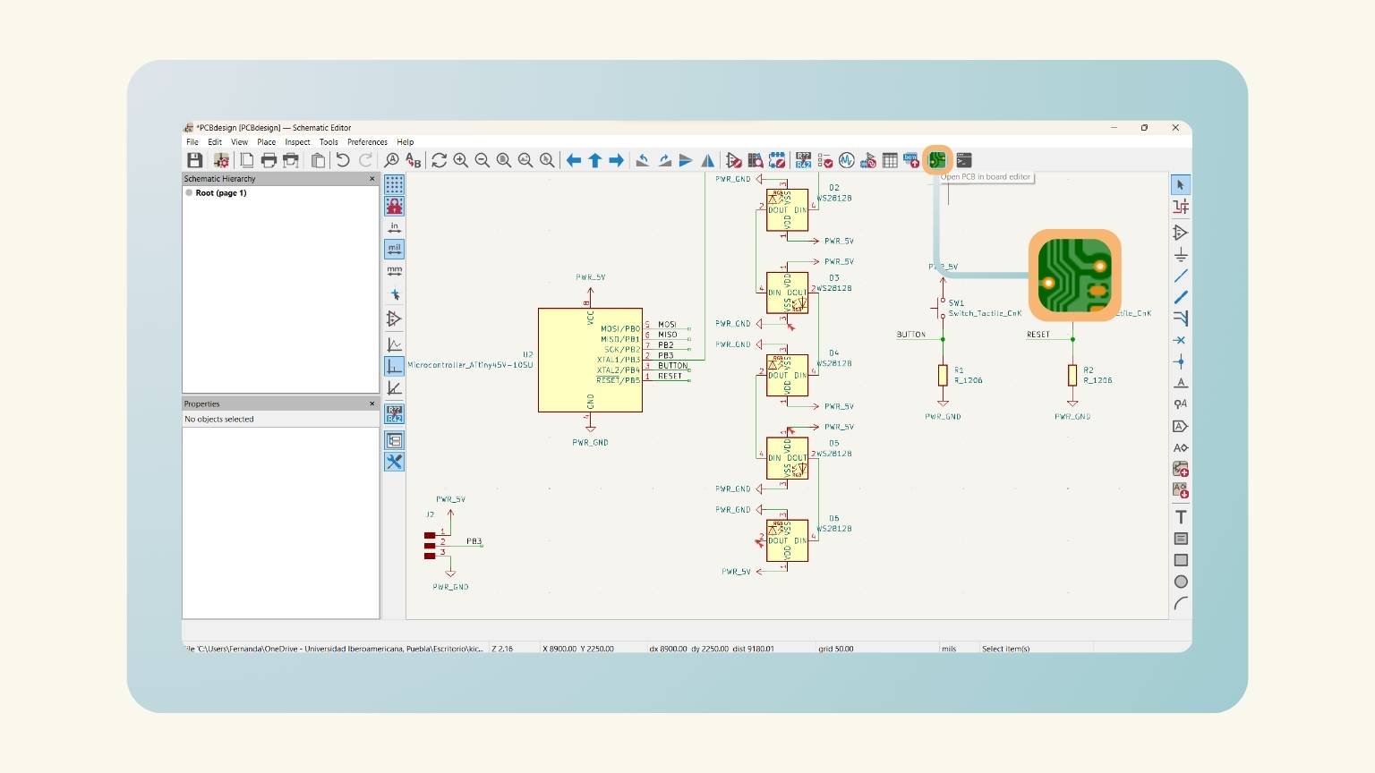
- Next, I returned to KiCad and pressed the option of ‘Open PCB in board editor’.
- The PCB Editor was open
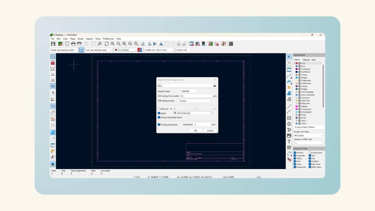
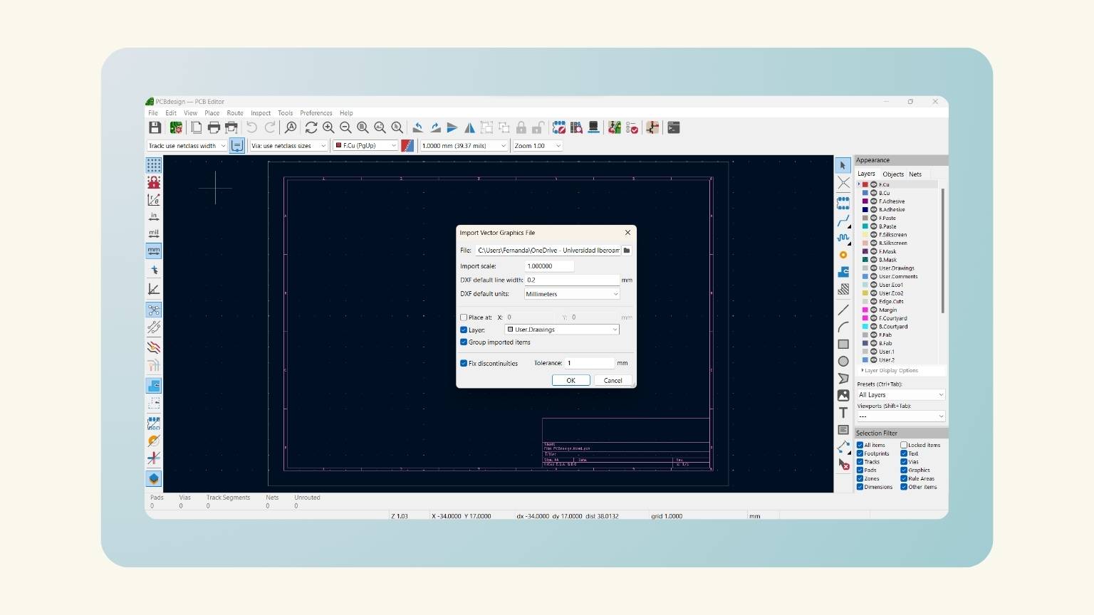
- I opened the ‘File’ and found the ‘Import’ option to add a graphic with the ‘Graphics…’ option.
- First, I selected the file.
- Then, I verified the predetermined parameters and pressed ‘OK’.
- I colocated the graphic in the workspace.
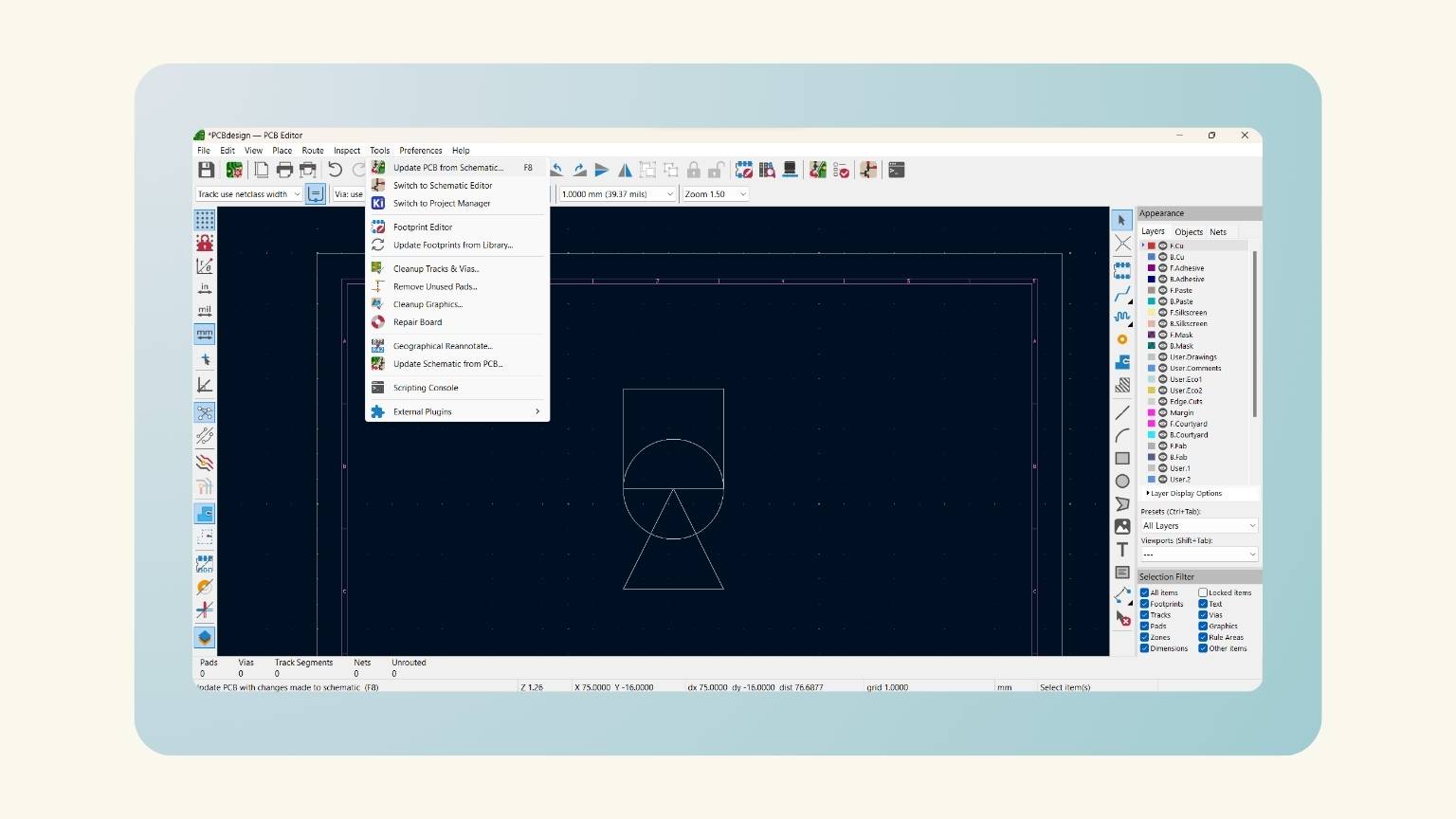
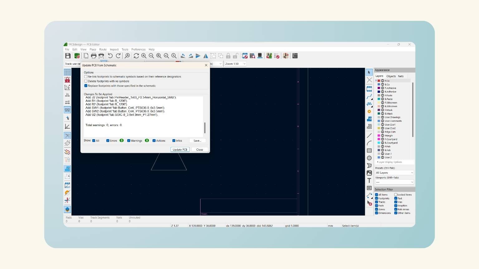
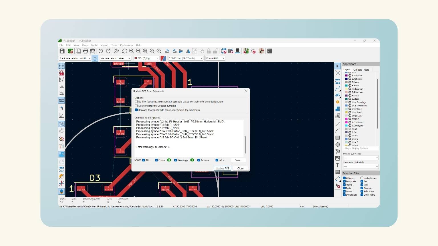
- After I pressed the ‘Tools’ menu and selected the ‘Update PCB from Schematic…’
- A window appeared where you could view the changes made to the schematic to be added to the PCB editor.
- I pressed the ‘Update PCB’ option.
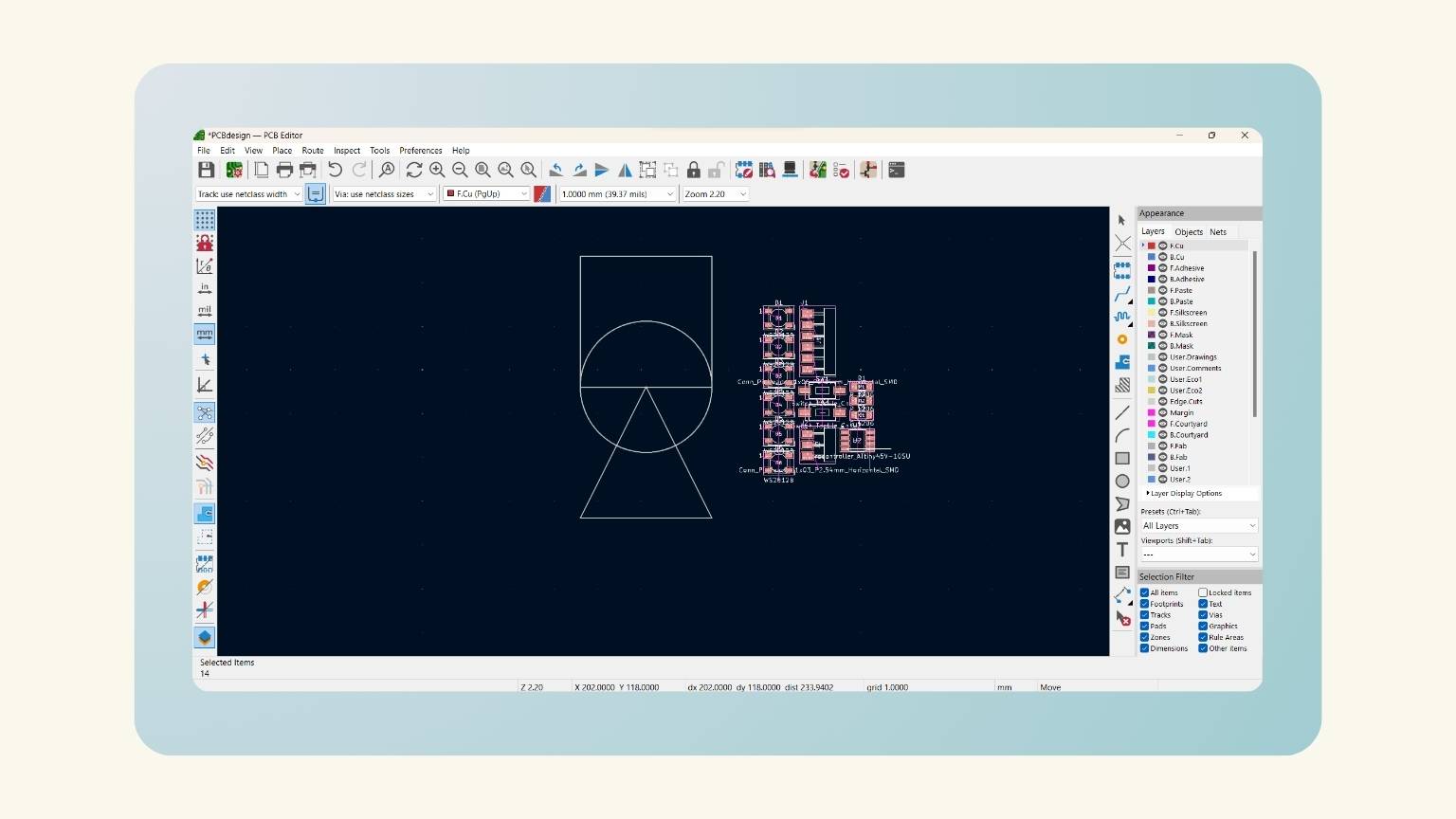
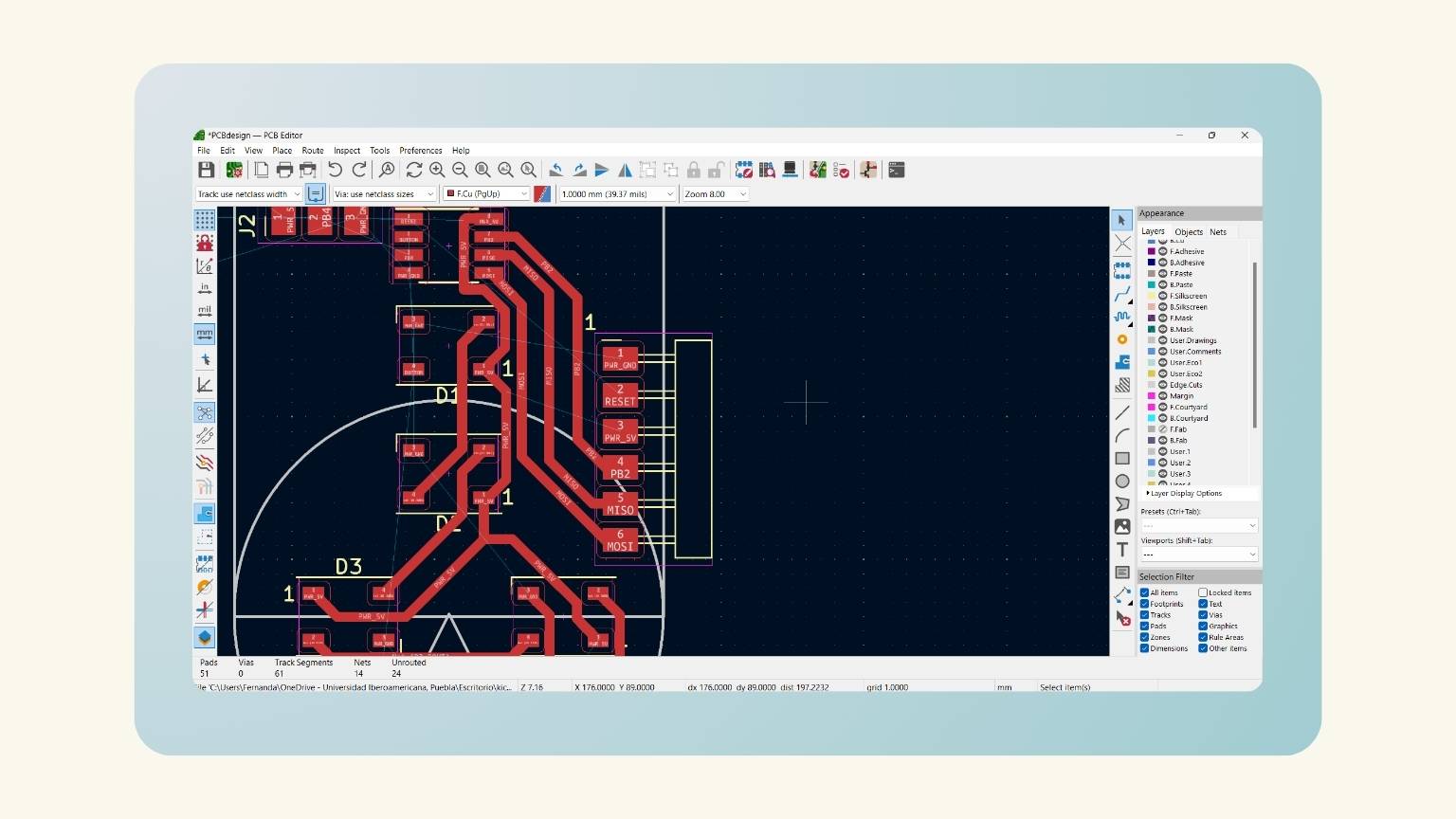
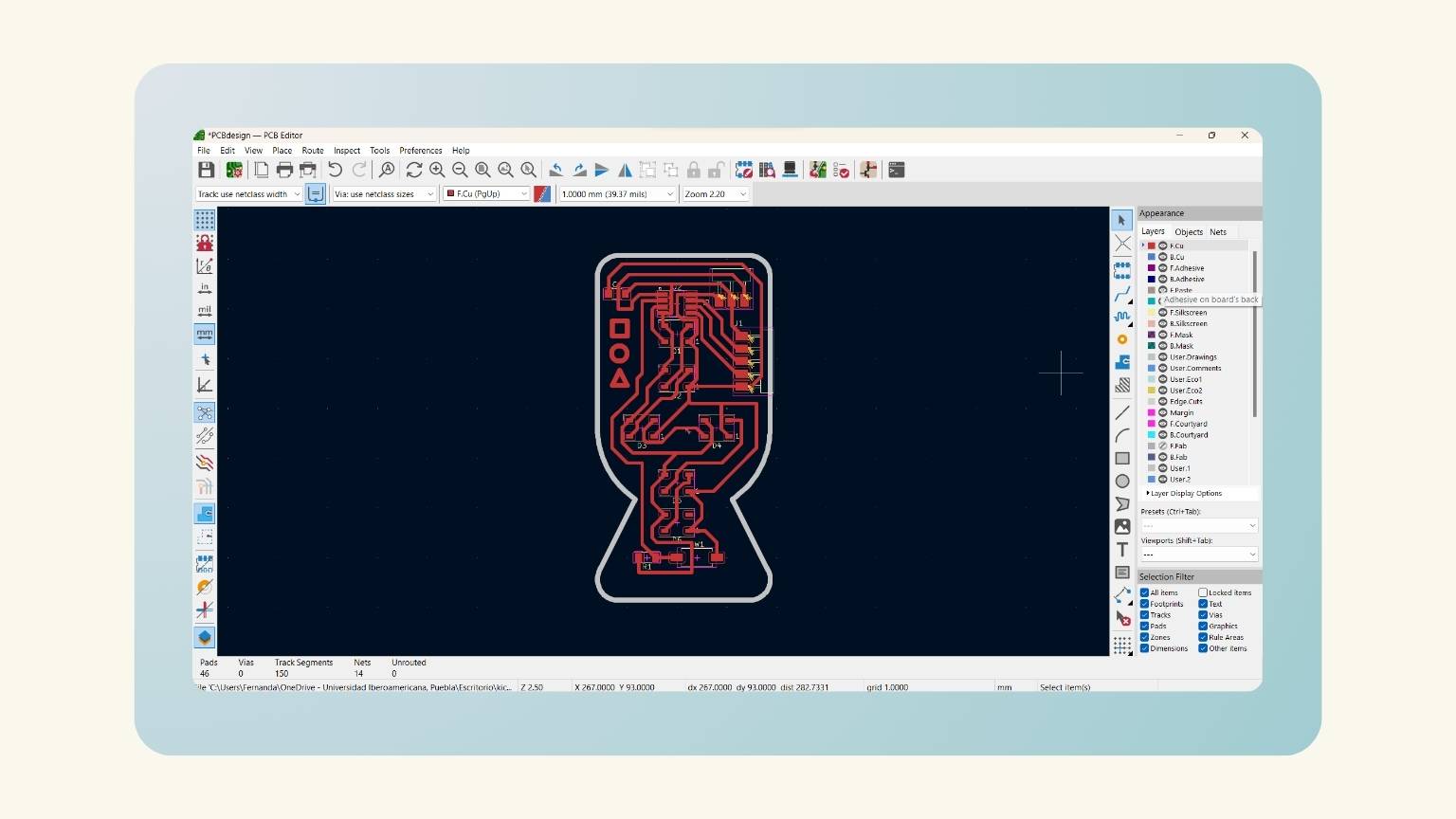
- I collocated the components in the workplace.
- I started to accommodate the components, taking as a reference the dxf file.
- As I was arranging, I was realizing that some connections could go differently to make the arrangement efficient and achieve the necessary connections. For this, I went back to the schematic to make the corrections.
- In order for the corrections made in the schematic to be reflected in the ‘PCB editor’, I went back to the ‘Tools’ menu to open the option of ‘Update PCB from Schematic…’ to update the PCB.
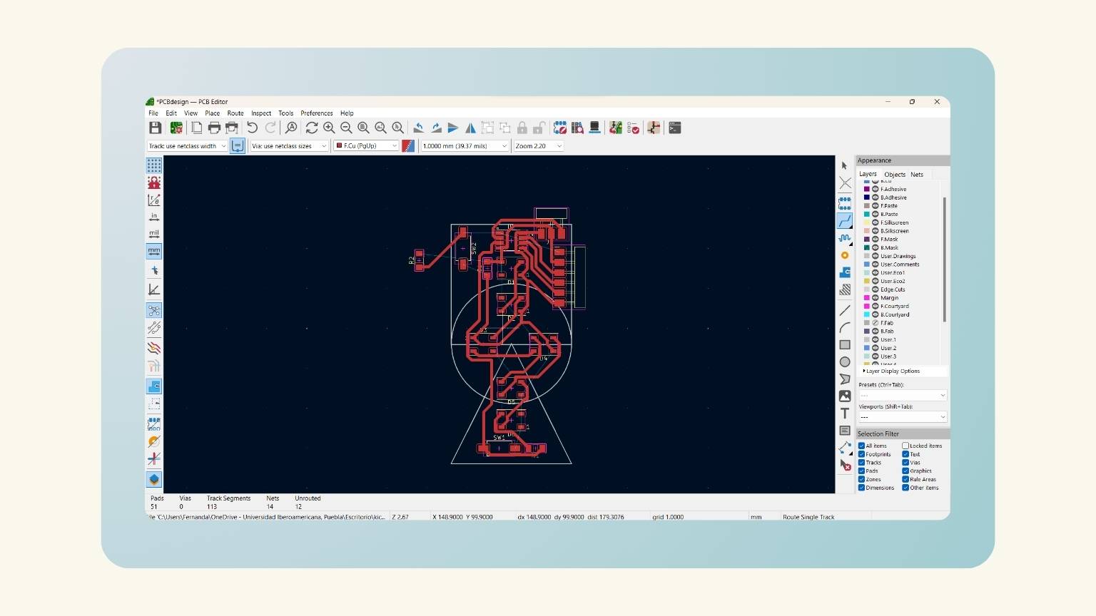
- And the changes were reflected.
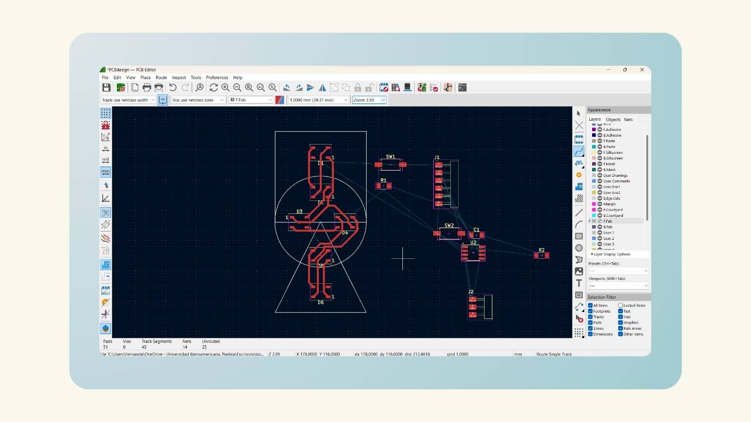
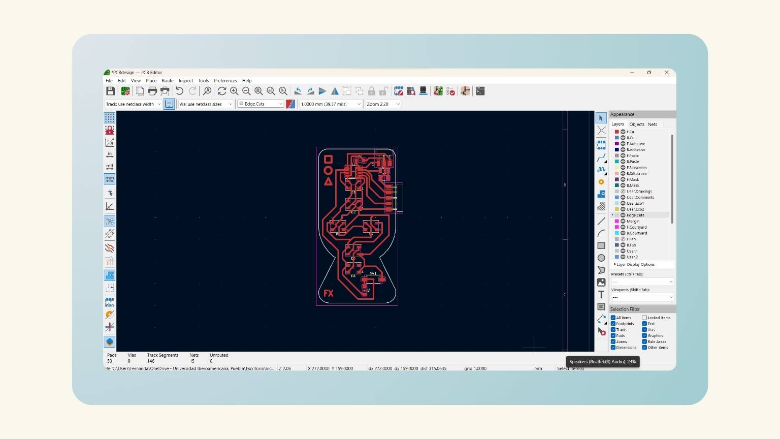
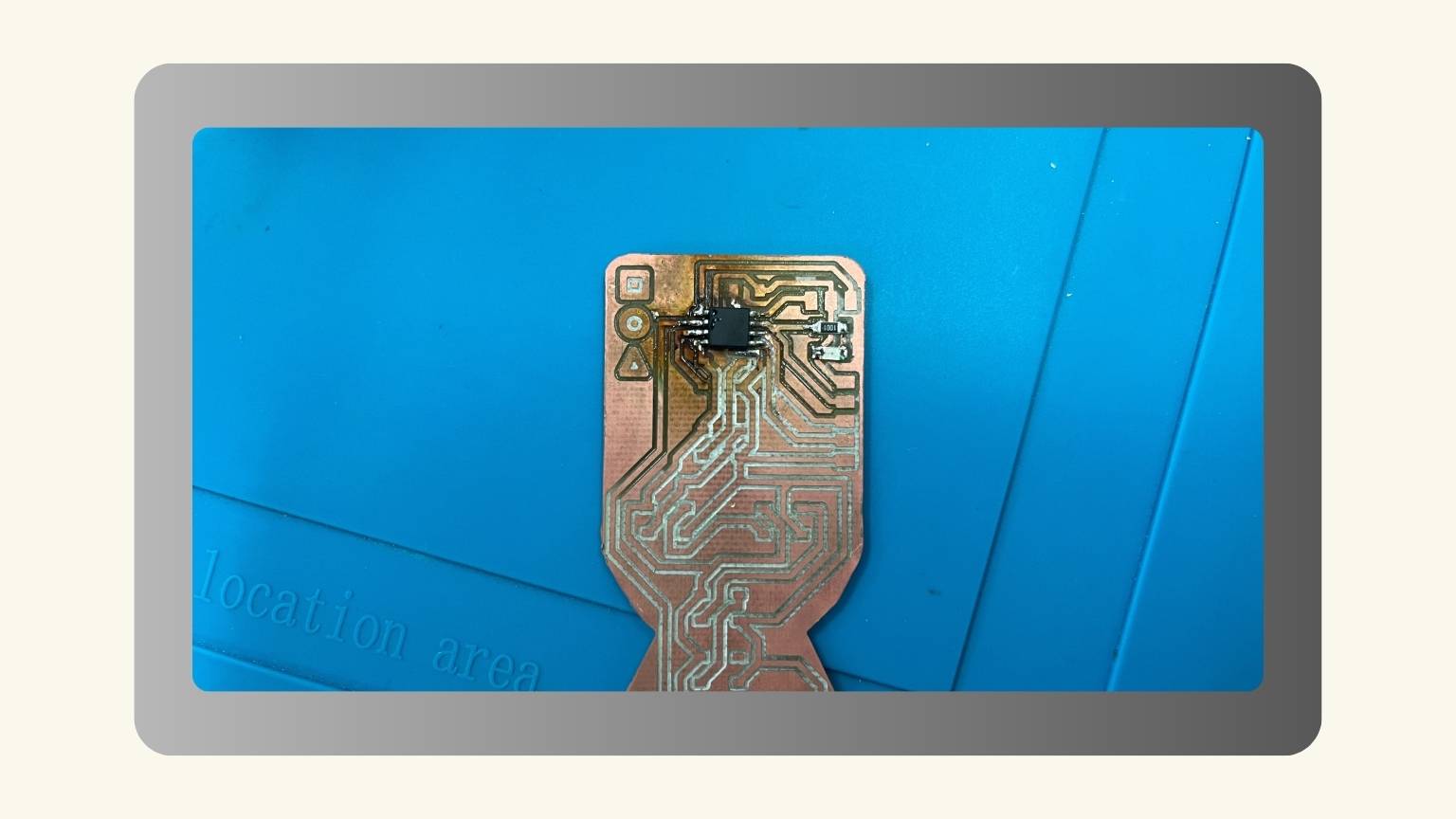
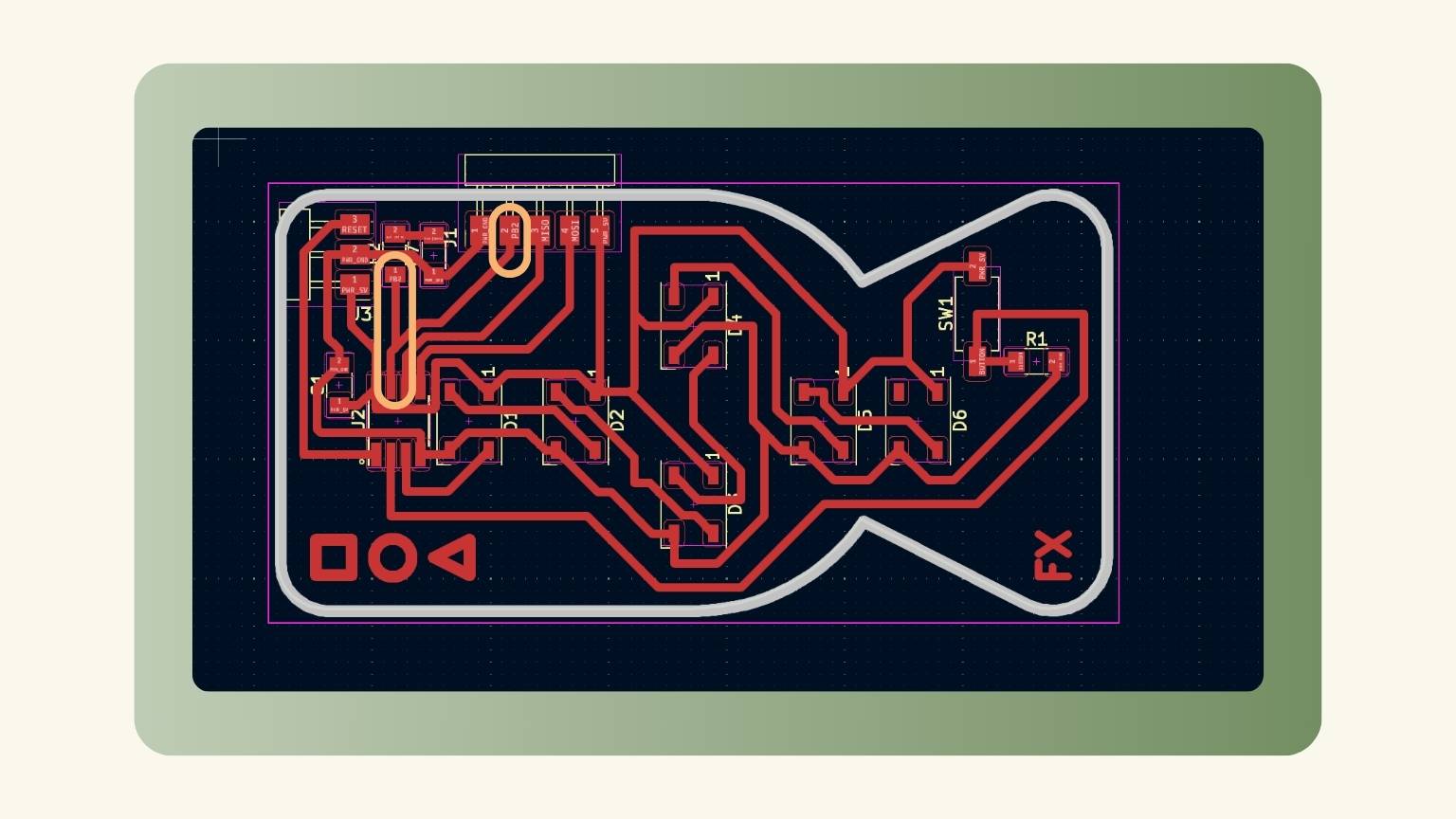
- After a lot of changes… the PCB looked like this and was already finished.
- At this point, I decided to delete the reset button and used a pin to do that.
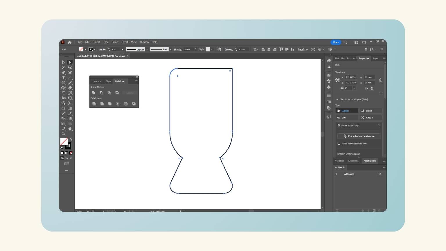
- I designed my frame to cut my PCB; do you remember that I made a square, circle, and triangle for my concept and design?
- So, I made on the triangle some fillets with a radius of 4 mm in the corners.
- Then, I used the ‘Unit’ pathfinder tool to make one shape of the three that I have.
- I made in the upper corners a fillet of 4 mm to make the shape more aesthetic.
- And I have the frame to cut my PCB!
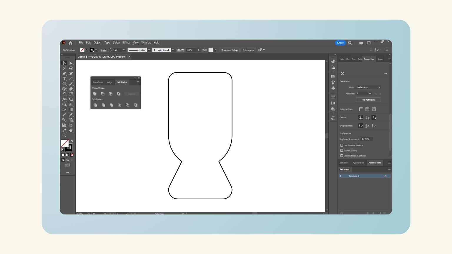
- I realized the last modifications, and I made the tinker contour to verify that it doesn’t interfere with any component.
- I added a LED and its resistor to use it as proof that the PCB is working when programming it.
- And this was the result of the design!
- In this design, I changed the location of the capacitor to have it closer to the components.
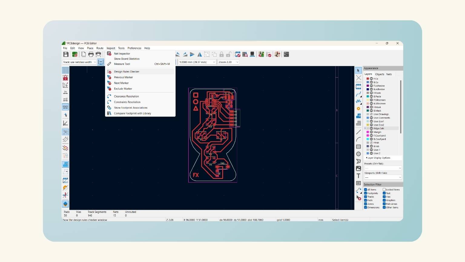
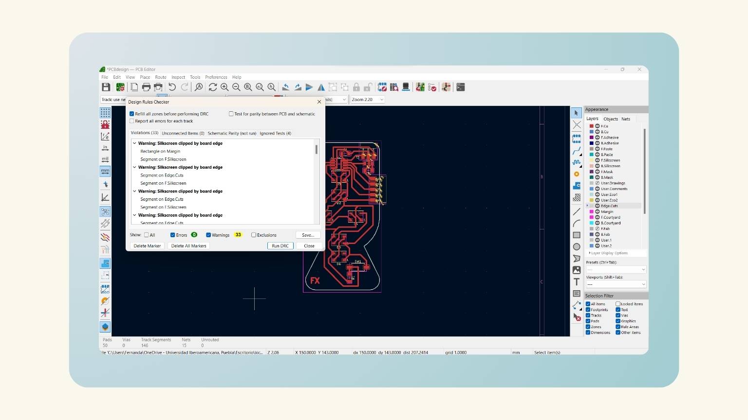
- To verify, I went to the ‘Inspect’ menu, specifically the ‘Design Rules Checker’ option.
- I pressed he bottom next to close, ‘Run ERC’, to see the mistakes, Then, I visualized the errors to correct them and verify if everything was okay.
Fab Libraries
Board Design
Frame Design
Back to KiCad


Cut Frame

The last steps
PCB Production
Lets make a recap of the week 04
The machine used for the creation of the PCB is...
ROLAND SRM-20
This machine can cut a broad range of materials, including chemical wood, acrylic, and ABS. It also supports a wide variety of accuracy settings, from prototype to product design. Furthermore, its tiny size and fully enclosed design allow you to cut with greater safety and confidence.
What tools will we use?
V-Cutter, allows for better engraving for its fine tip.
Flute end Mill, for drilling and plate cutting.
To prepare the control software, I used...
Mods
A program that allows me to extract G-codes or machine codes from images, vectors or 3d models.
So, when I have my PCB design, I have to save it…
but how did you save it?
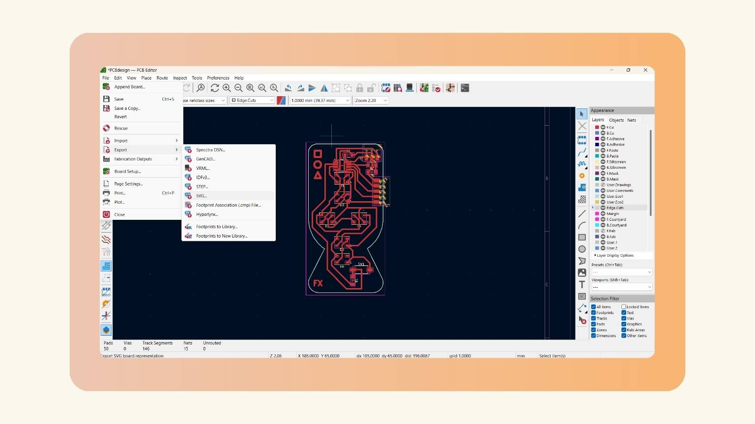
- I went back to the KiCad PCB Editor and went to the ‘File’ menu, subsequently to 'Export', and selected the ‘SVG’ option.
- The ‘Export’ menu was displayed, and I selected the layer I wanted to save. In this case, I first saved the strokes that were inside the
‘Copper layers’, which have the name ‘F.Cu’.
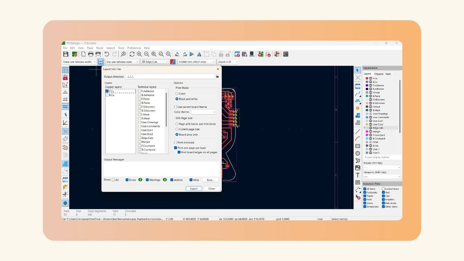
- In the options, I selected the ‘Black and white’ print mode and the ‘Board area only’ SVG Page Size. Then I pressed ‘Export’.
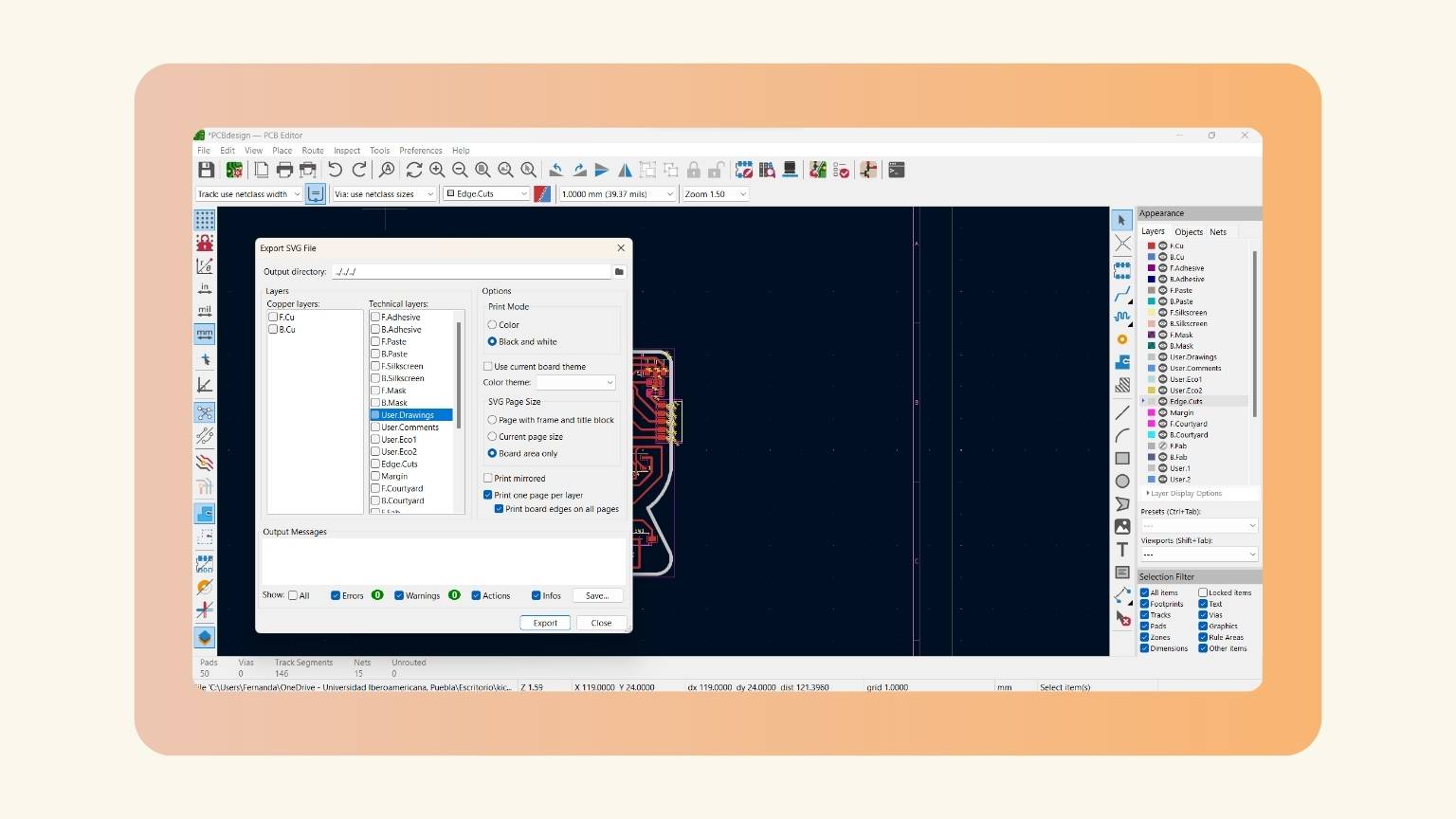
- After, I did the same, but I changed the strokes layer to the cut later; in my case, it was the ‘User.Drawings’ layer.
- And I have the two files to cut!
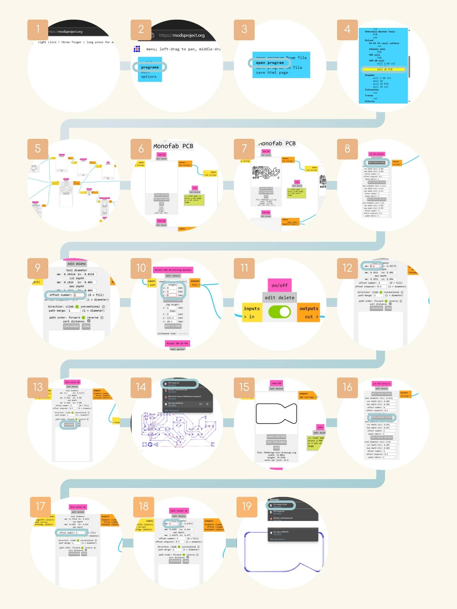
Mods Time
- I opened the MODS web server.
- I right clicked on ‘Programs’
- Next in ‘Open program’
- I searched the program of the SRM-20 mill machine and selected the ‘mill 2D PCB’.
- All the blocks to be worked on are displayed to obtain the corresponding files.
- The first block that I modified is the 'read SVG’ block for selecting a SVG file.
- I saw that the image was uploaded to the server.
- I moved to the ‘set PCB defaults’ block and pressed ‘mill traces’.
- I moved to the ‘mill raster 2D’ block. And I changed the ‘offset number’ to two.
- Then, I went to the ‘Roland SRM-2D milling machine’ block, and I modified the origin of the machine. For this, I changed the numbers on the axes x, y, and z.
- I moved to the right and turned on the ‘outputs’.
- I moved to the ‘mill raster SD’ and changed the tool diameter to 0.4 mm.
- And then I pressed ‘calculate’.
- And I saw a preview. In addition, in my downloads, I found an archive ‘.png.rtl’; this is the file that I opened on the machine.
- Next, I did the same steps with the SVG of the cut. Starting by selecting the cut SVG of my files.
- I moved to the ‘set PCB defaults’ block and pressed ‘mill outline’.
- Then, I went to the ‘mill raster 2D’ block and changed the ‘offset number’ to one.
- I moved to the ‘mill raster SD’ to change the tool diameter to 1 mm.
- And I pressed calculate to see the preview of the cut and downloaded the file for the machine.
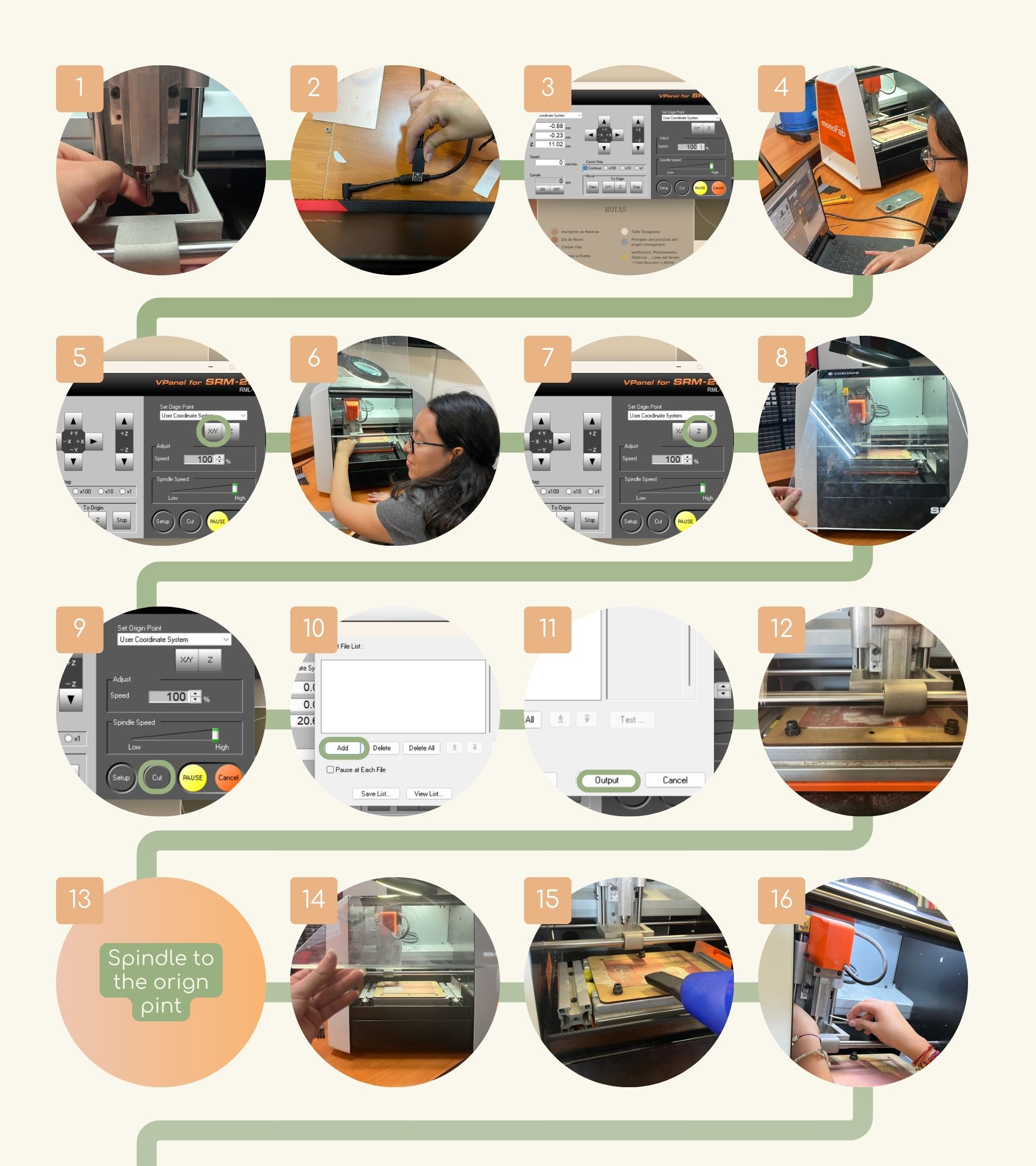
Cut Time
- I placed the tool, a 15 degree V-bit, to make the engraving.
- To do this, I used a wrench to tighten the tool.
- Note:Make sure that only the conical part of the tool protrudes.
- I connected the machine to my computer.
- I open the ‘VPanel for SRM-20’
- First, I moved the X/Y axis to the lower left of the material.
- And I pressed the ‘X/Y’ bottom to change the origin of this axis’s.
- Then, I moved the Z axis. To do this, I used a piece of paper to make sure I put the axis at the correct height.
- For this special axis, I used a paper to define the distance between the tool and the material. I did this by placing the paper on the material and lowering the tool a little at a time until the point where friction is generated and the paper gets stuck.
- Note: In this axis, before we did the paper check, we had to turn on the spindle and lower the z-axis, giving only one click to selecting ‘x10’ in the cursor step.
- I save the origin of the axis by pressing ‘Z’.
- When I defined the axis of origin, I closed the door of the machine.
- Then, I pressed the 'Cut' button at the bottom of the panel.
- I added the file to be engraved.
- I pressed ‘Outpt’ to send the file to be engraved.
- And the machine started to engrave.
- When the engraving was finished, the spindle went to the origin point.
- I opened the door of the machine.
- I used a hand vacuum cleaner to remove the dust produced by the engraving.
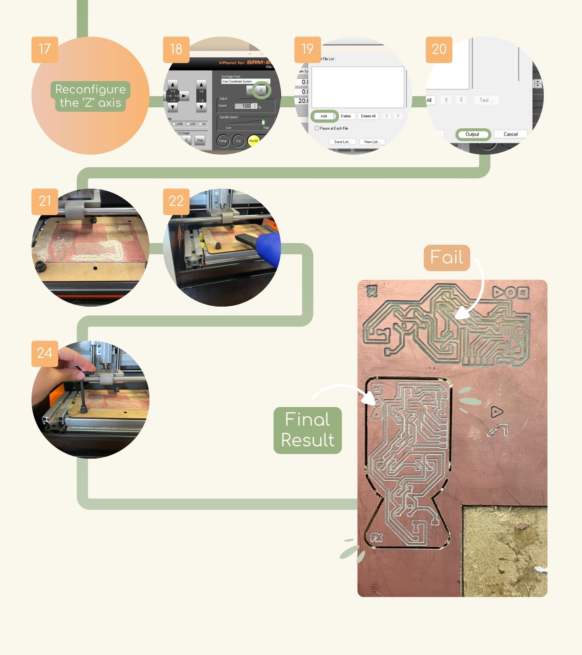
- I removed the tool that the machine had because it wasn’t the right one.So, I changed the previous tool to do the cut.
- For this, I used a wrench to tighten the tool.
- Note:Make sure that the conic part protrudes.
- I maintained the ‘X/Y’ origin and only changed the ‘Z axis’ because the tool was different and it was necessary to reconfigure that axis due to the height of the tool.
- I save the new origin of the axis by pressing ‘Z’.
- When I closed the door of the machine, I pressed the ‘Cut’ button to delete the previous file that I added.
- I added the new file of cut. And I pressed ‘Output’ for the machine to execute the cut.
- The machine started the cut.
- I used a hand vacuum cleaner to remove the dust produced by the cut.
- I removed the screws fixing the material with the help of a screwdriver.
- Finally, I had my card burned and cut.
Note:To move the axis fist, I used the ‘Continue’ cursor step, after the ‘x100’ (1 mm), then the ‘x10’ (0.1mm), and finally the ‘x1’ (0.01mm) until the paper generated friction and didn’t come off.
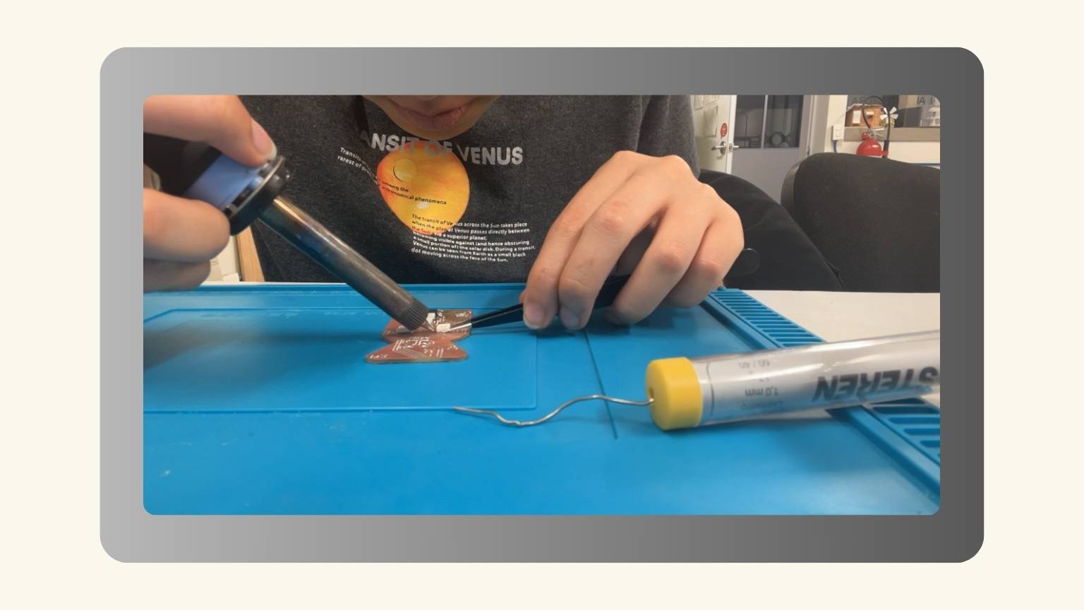
Soldering... my old friend
In this part, chaos started.
So, what happened?
First, I did a little practice with the tracks that went wrong. This was my practice:
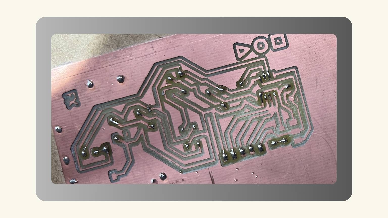 And I think that it was beautiful... and I was there to solder my PCB.
I started to solder the microcontroller, in this case the Attiny 85. And I ruined one of the tracks and burned some areas. So, I panicked because I’m new to that and don’t know if some things have a resolution or not.
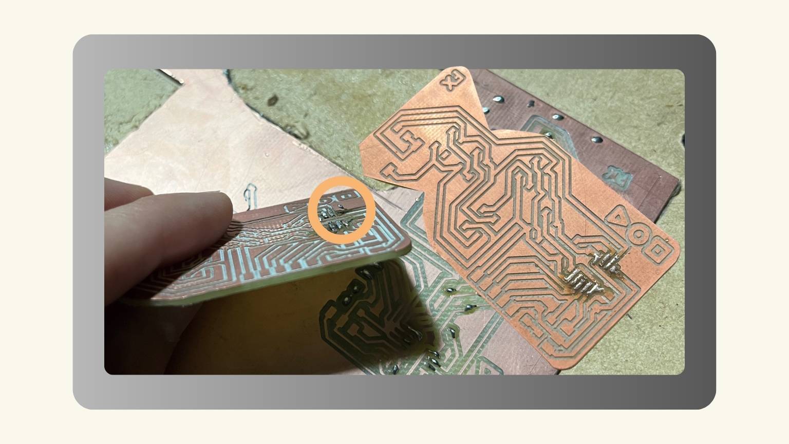
This happened on Sunday, and the next day wasn’t going to be a workday at Fab due to a Mexican holiday... and my panic increased.
So, I thought things over and decided to have an instructor analyze my PCB on Tuesday to tell me if I could fix it or make another one.
Also, analyzing it a bit, this was better, because if I soldered the other components and, in the end, the Attiny didn’t work, it was going to be a waste of work.
Tuesday came, and an instructor was able to check my board. He told me it would be best to redo it, but because of the time constraints, he helped me figure it out with what we had. My PCB was a little burned, but it worked.
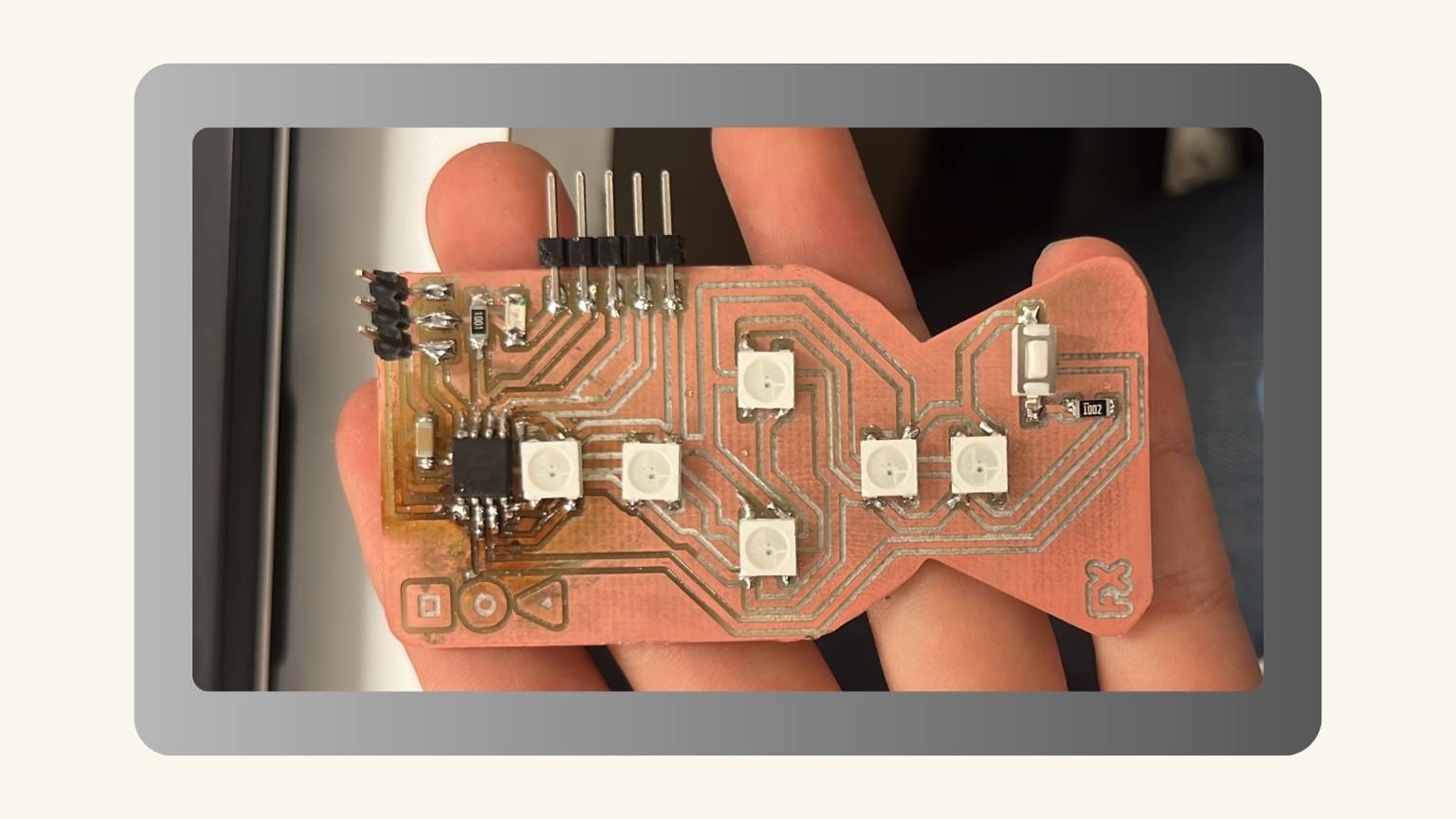
Next, I soldered the rest of the components.
Notes:
- The Neopixels were hard to solder.
- And I don’t know why, but the last three pines were too difficult. It took me about an hour trying to solder them
Finally, all the components were soldered!
Multimeter Test
What is a multimeter?
A digital multimeter (DMM) is a flexible electronic instrument that can test a variety of electrical characteristics such as voltage, current and resistance. The measurements are shown on a digital screen, making them easier to read and comprehend precisely.
So, I used this tool to check that all the connections were good.
Programming
- I opened Arduino.
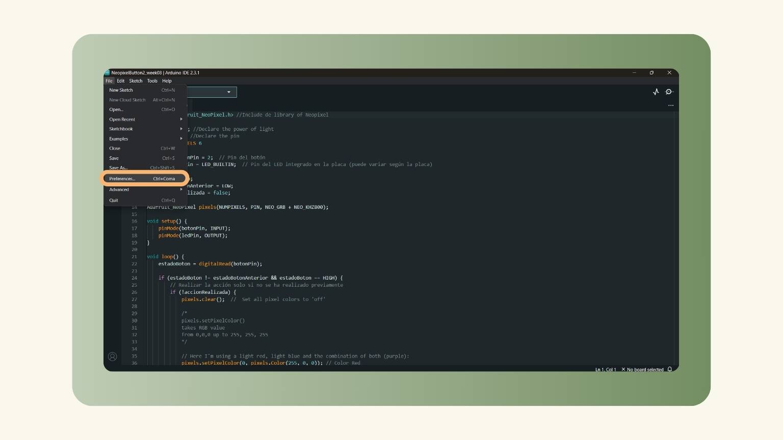
- I selected the ‘File’ menu and clicked on ‘Preferences’.
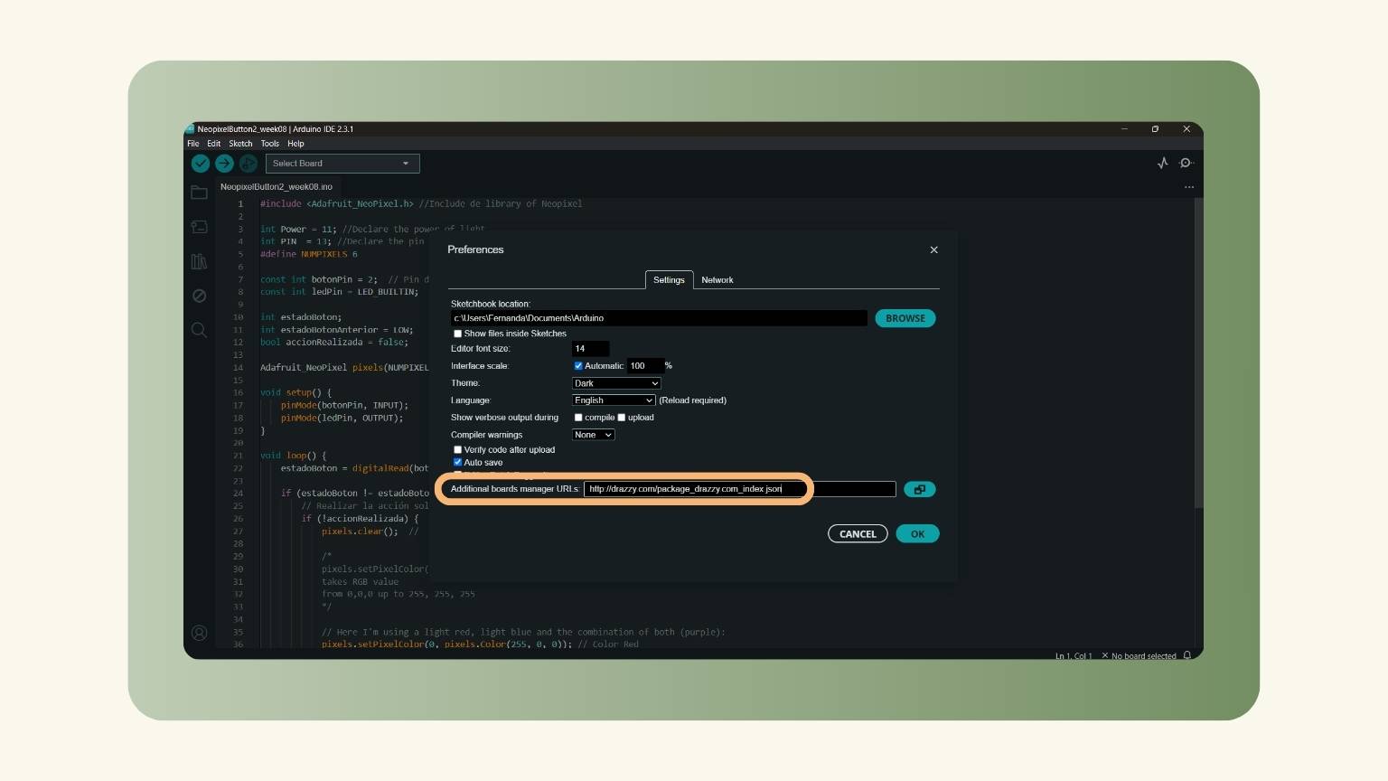
- Then I paste the next link to the section of ‘Additional boards manager URLs’. http://drazzy.com/package_drazzy.com_index.jso
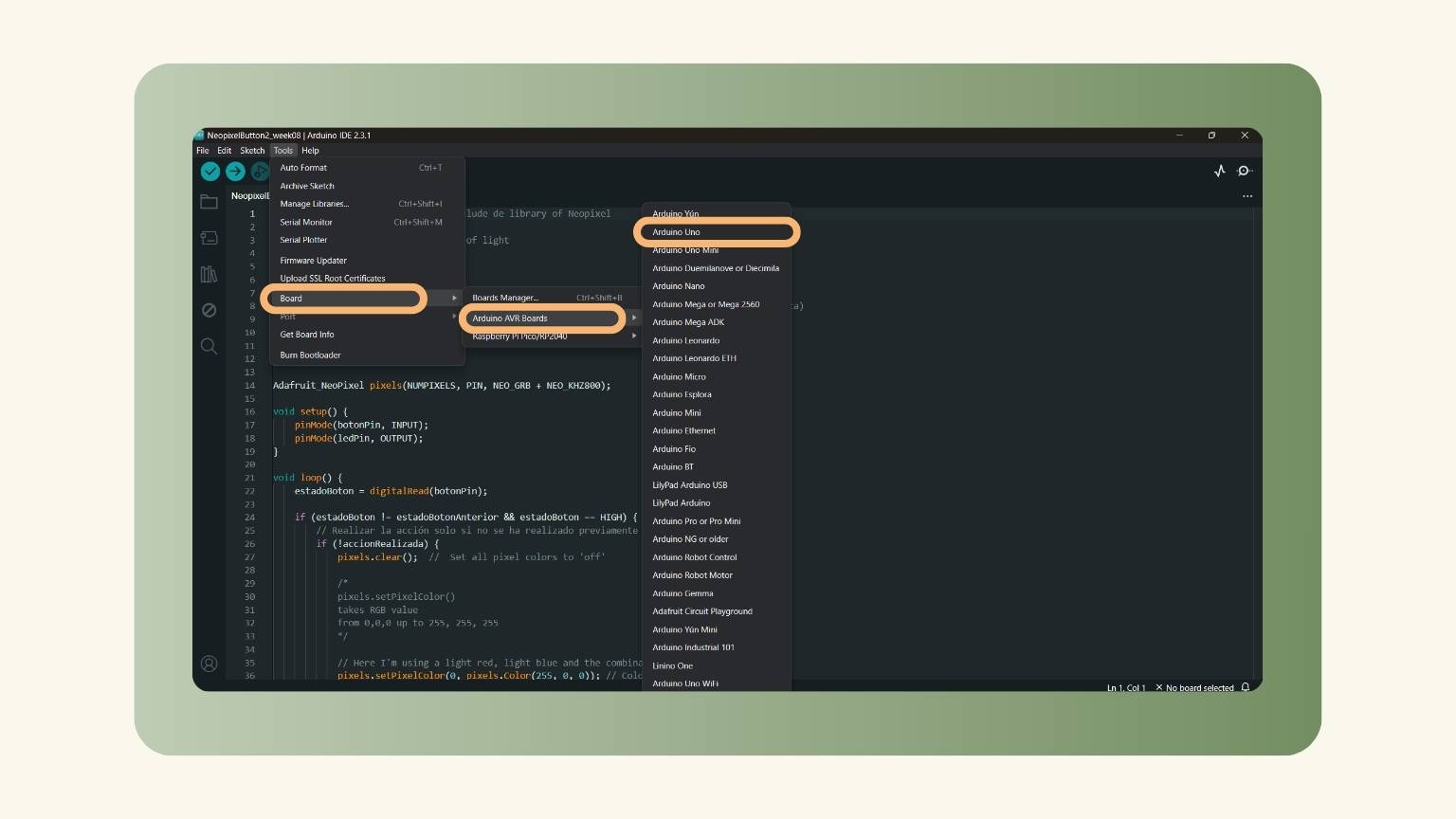
- I pressed 'OK', and then I went to the ‘Tools’ menu to select ‘Board’, after ‘Arduino AVR Boards’ and finally ‘Arduino Uno’.
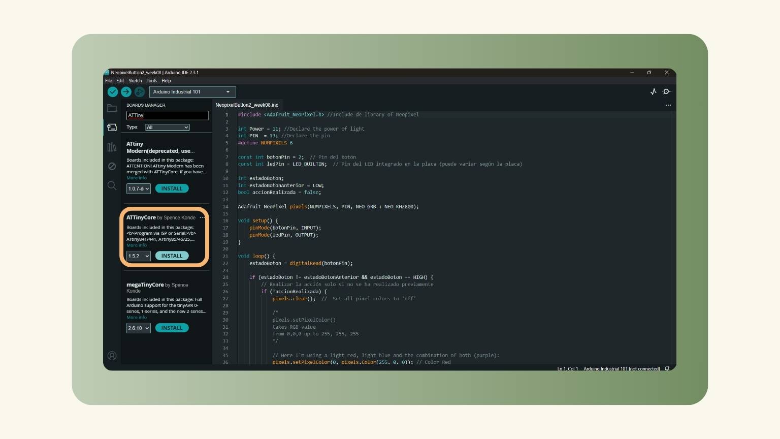
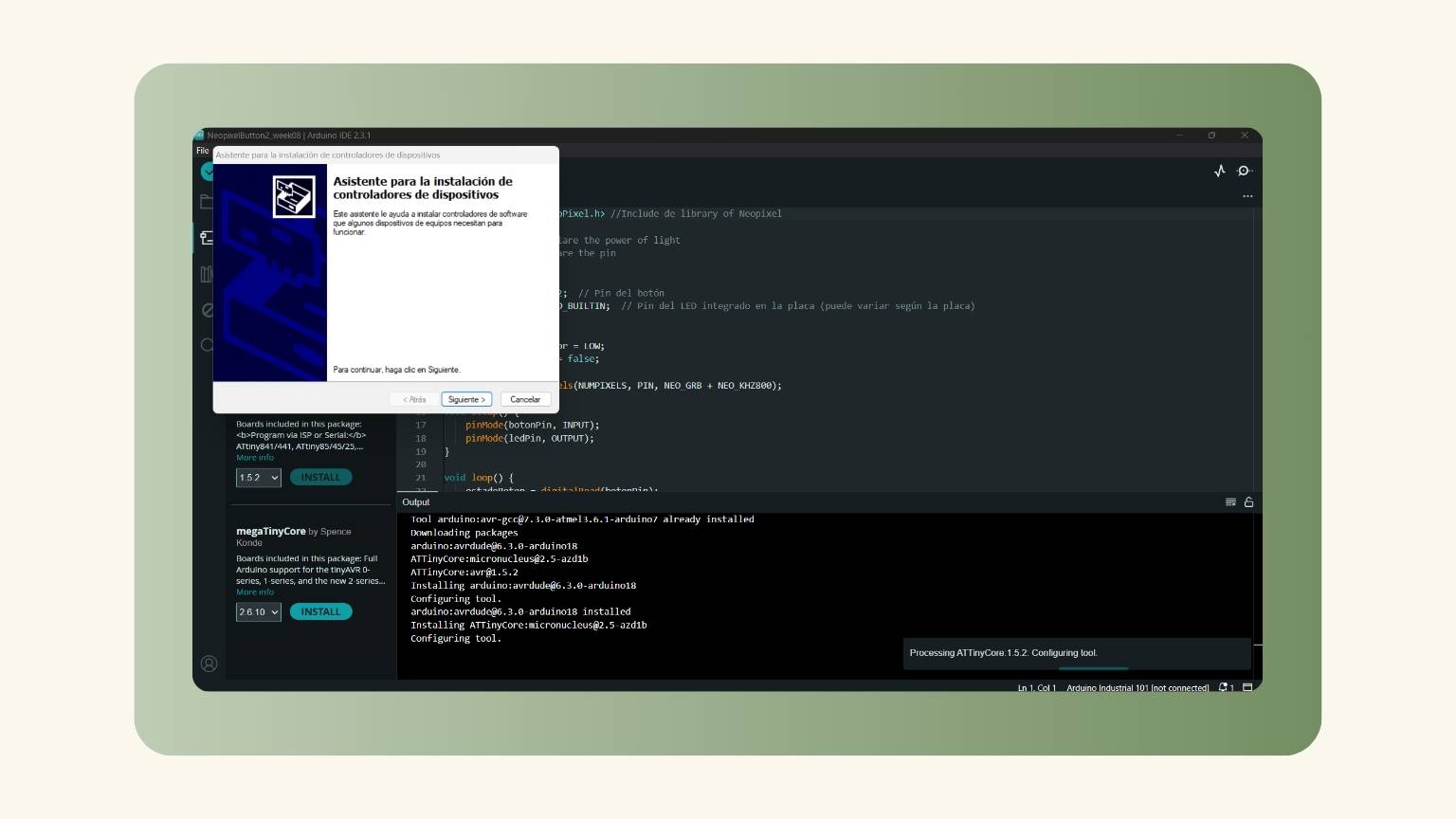
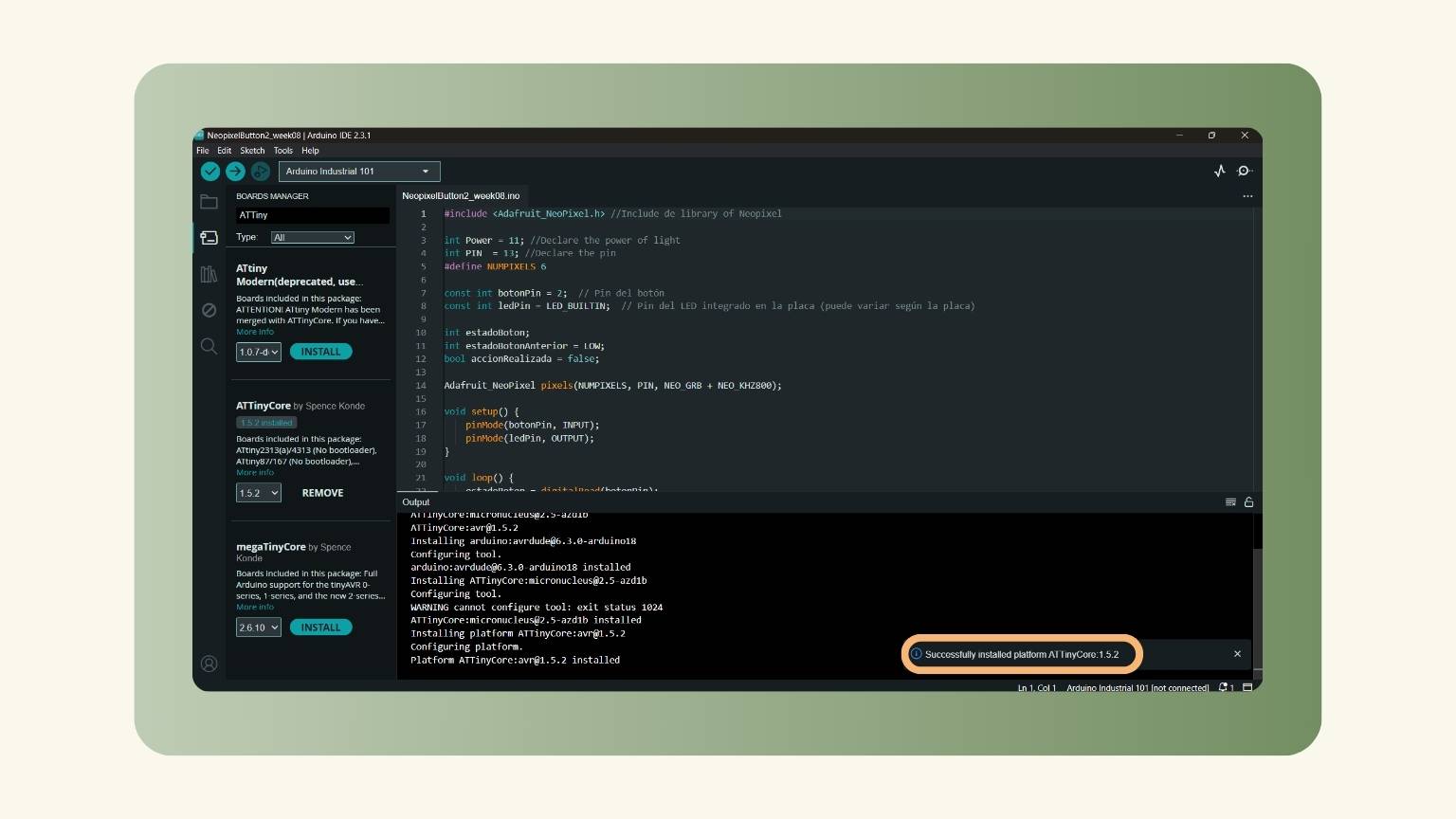
- I installed the ‘ATTinyCore’ library.
- I followed the steps to install.
- The installation was done.
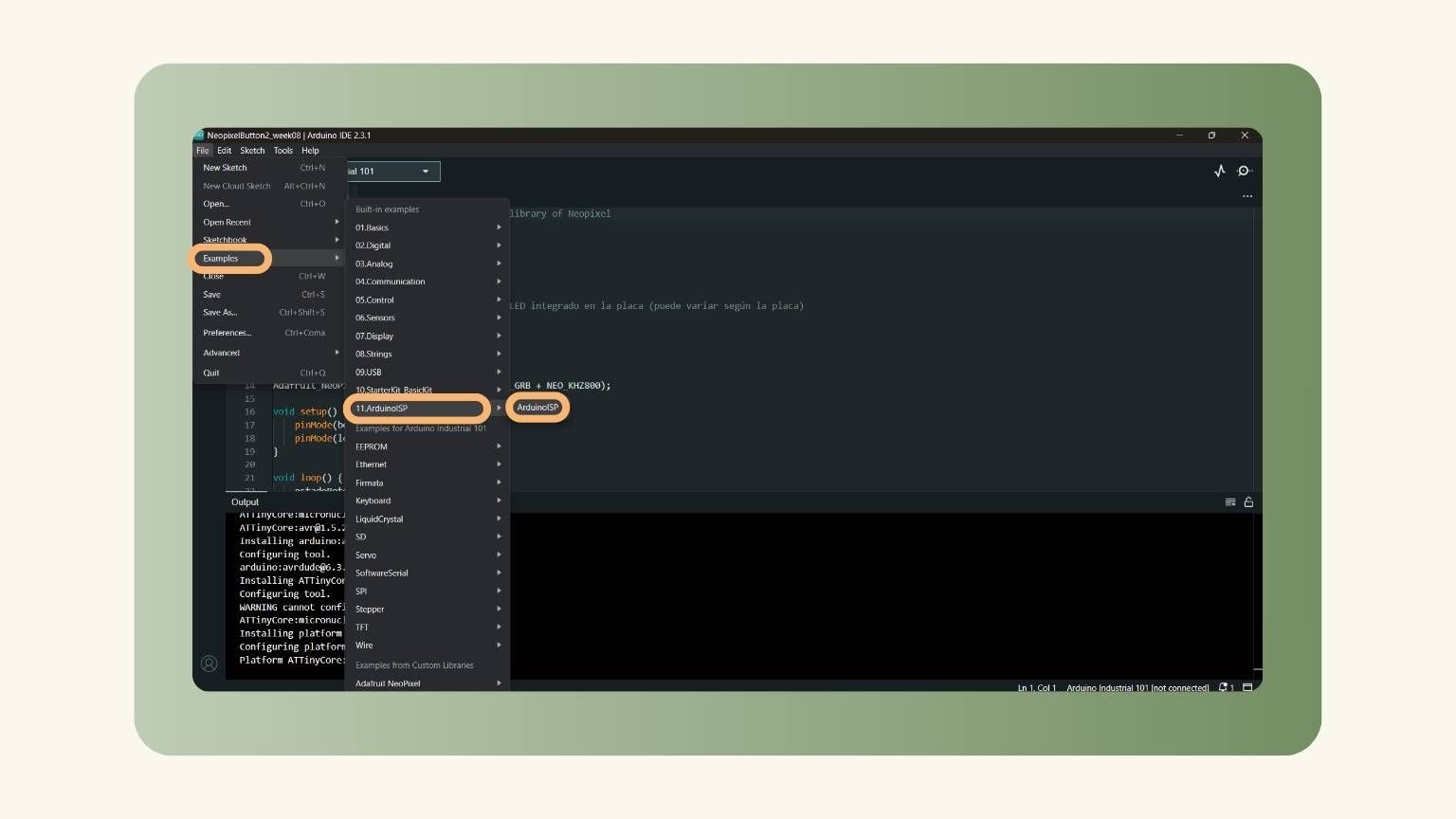
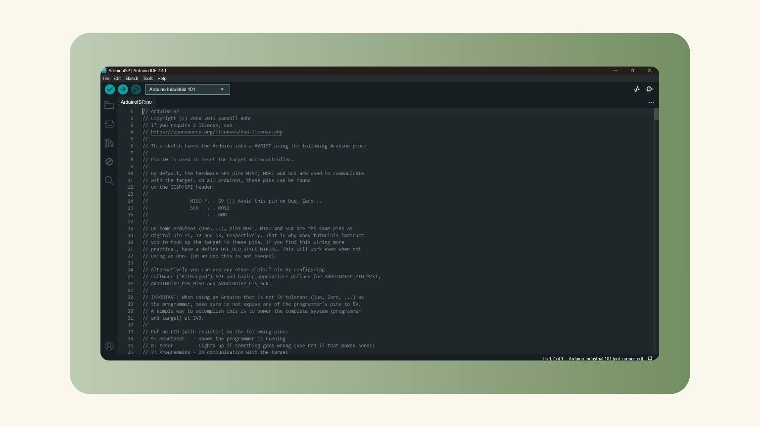
- Next, I went to the ‘File’ menu to open the example of ‘ArduinoISP’.
- The example was open.
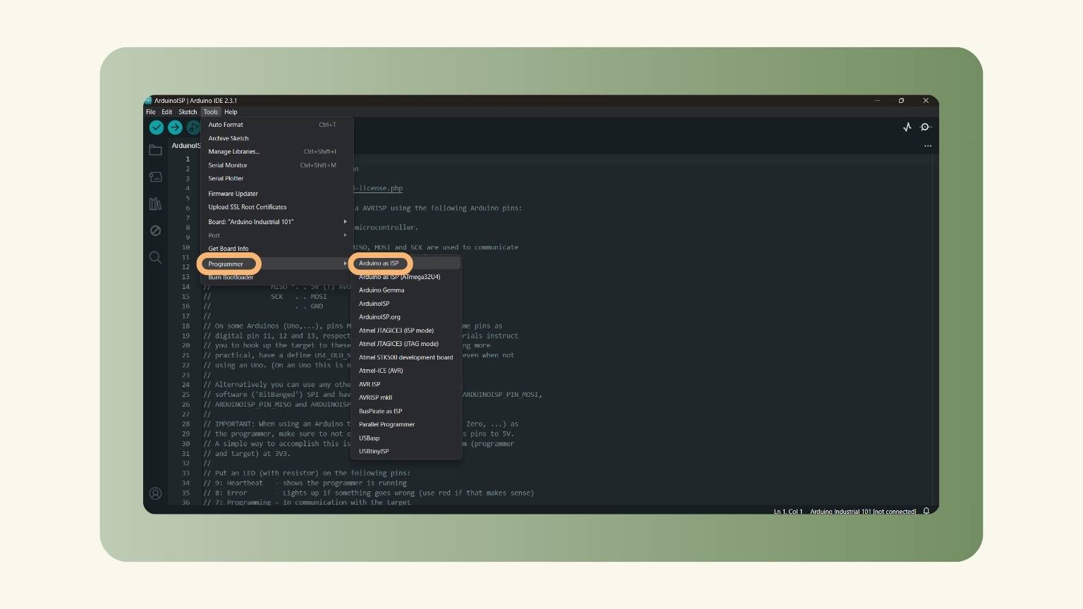
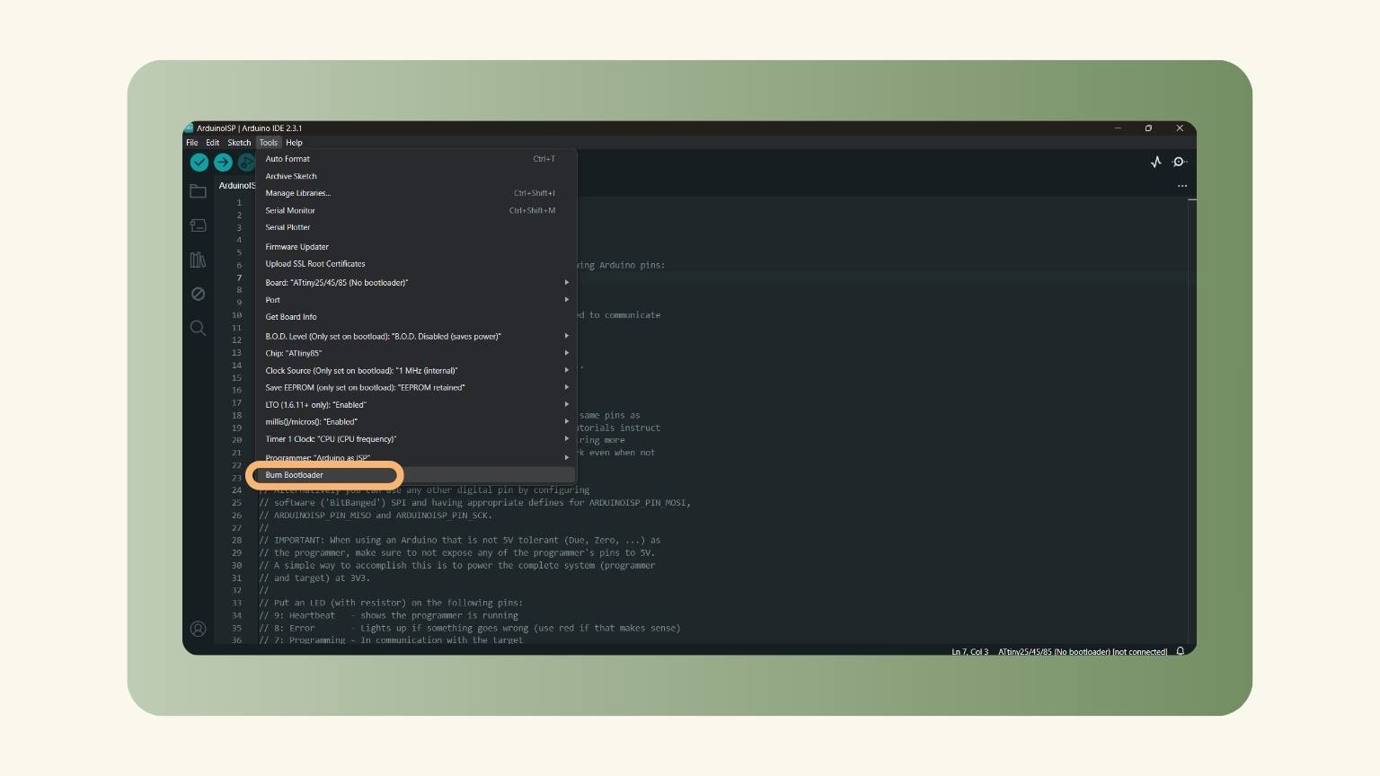
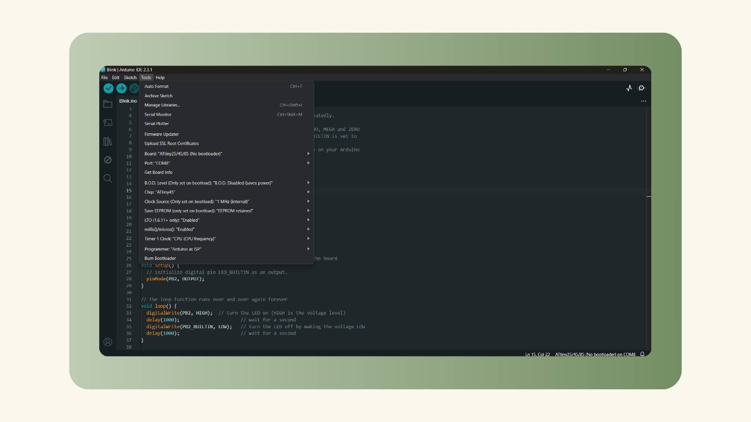
- I selected the ‘Tools’ menu to select the ‘Programmer’ option and pressed the ‘Arduino as ISP’.
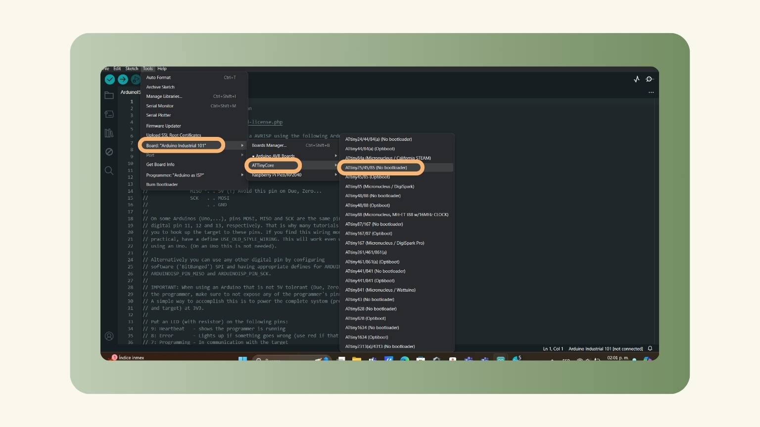
- Then, in the same menu, I selected the ‘Board: “Arduino Industrial 101”’ and chose the ‘ATTinyCore’ to specify the ‘ATtiny25/45.85 (No bootloader)'.
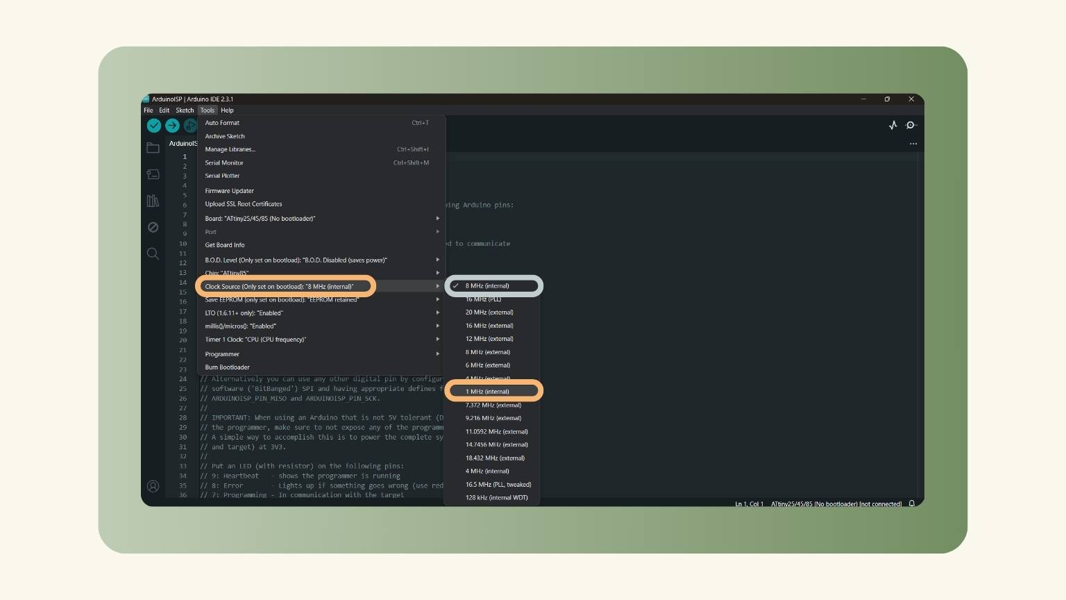
- I selected the ‘Clock Source’ option to select the ‘1 MHz (internal)’ option.
- Note: If you use Neopixel, you will change to ‘8MHz(internal)’.
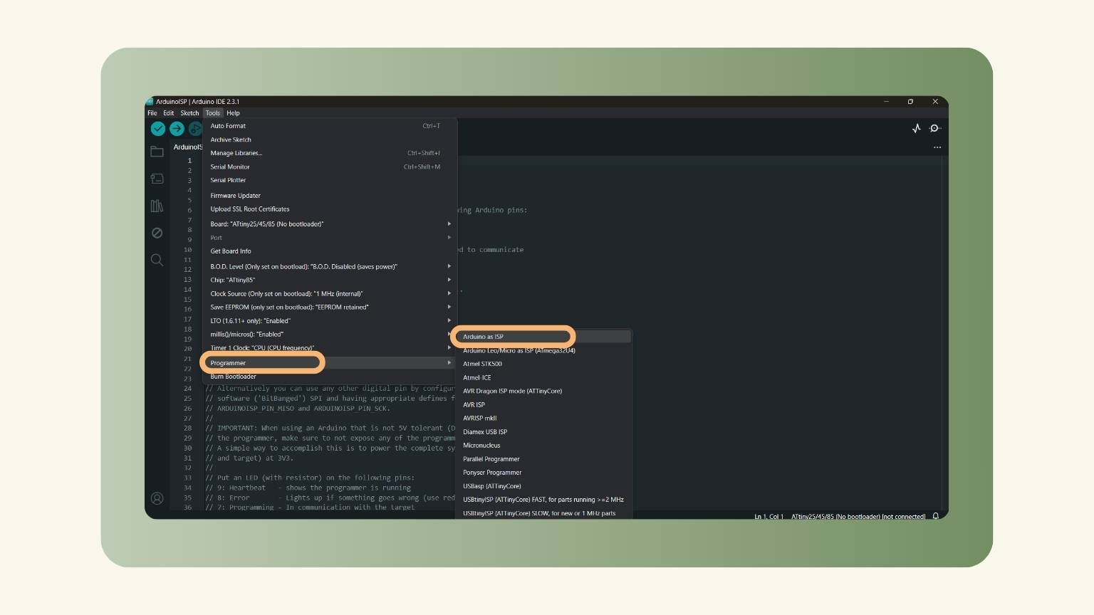
- I selected the ‘Arduino as ISP’ programmer in the ‘Tools’ menu.
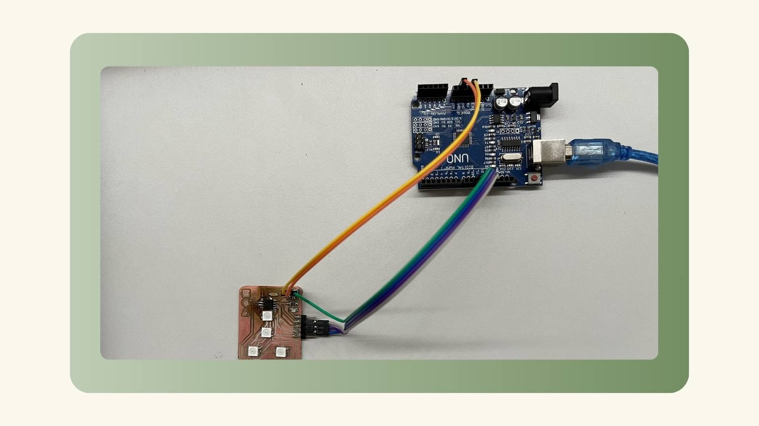
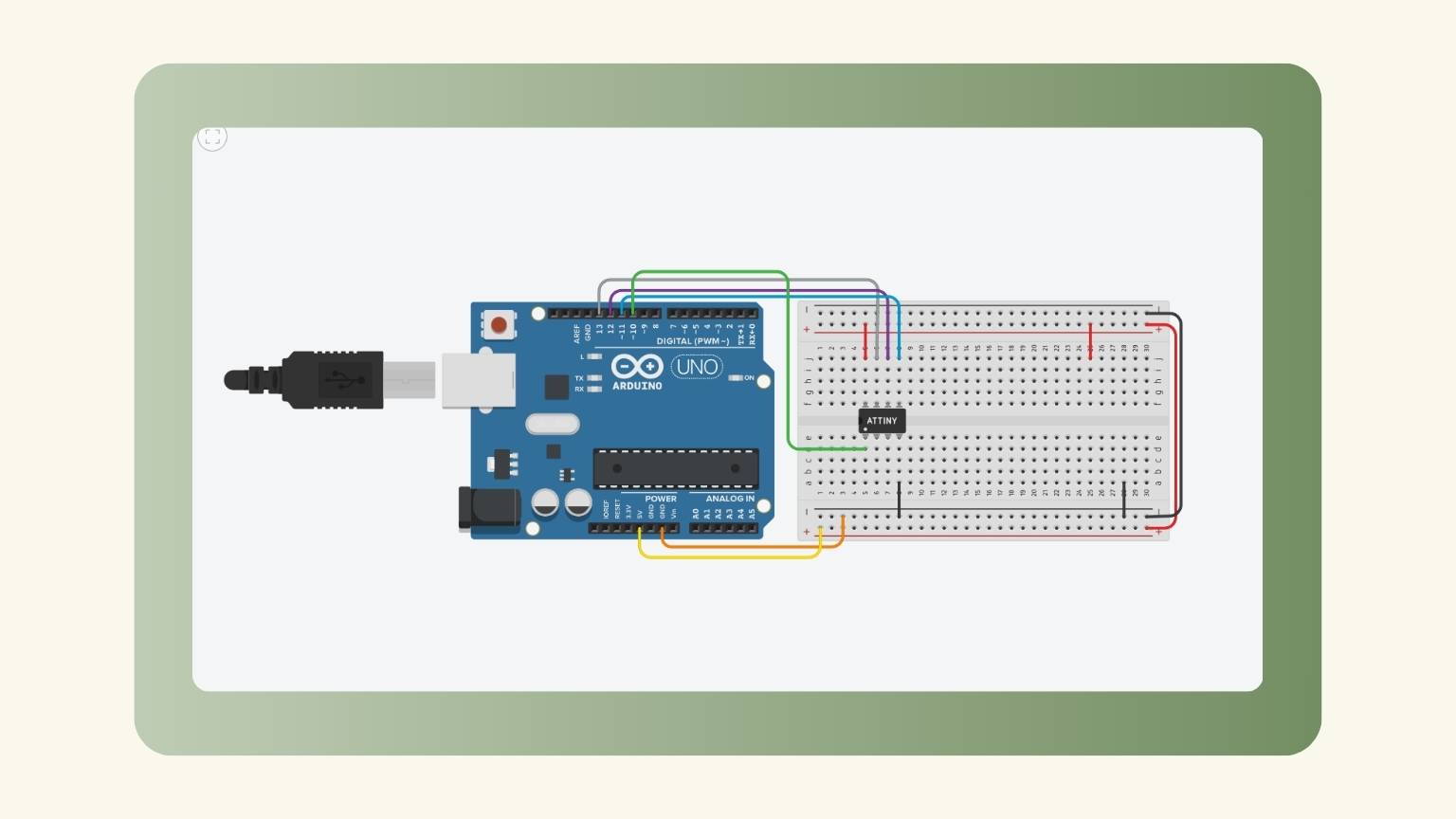
- I connected the Arduino to my PCB.
- I used this diagram to understand how to connect them.
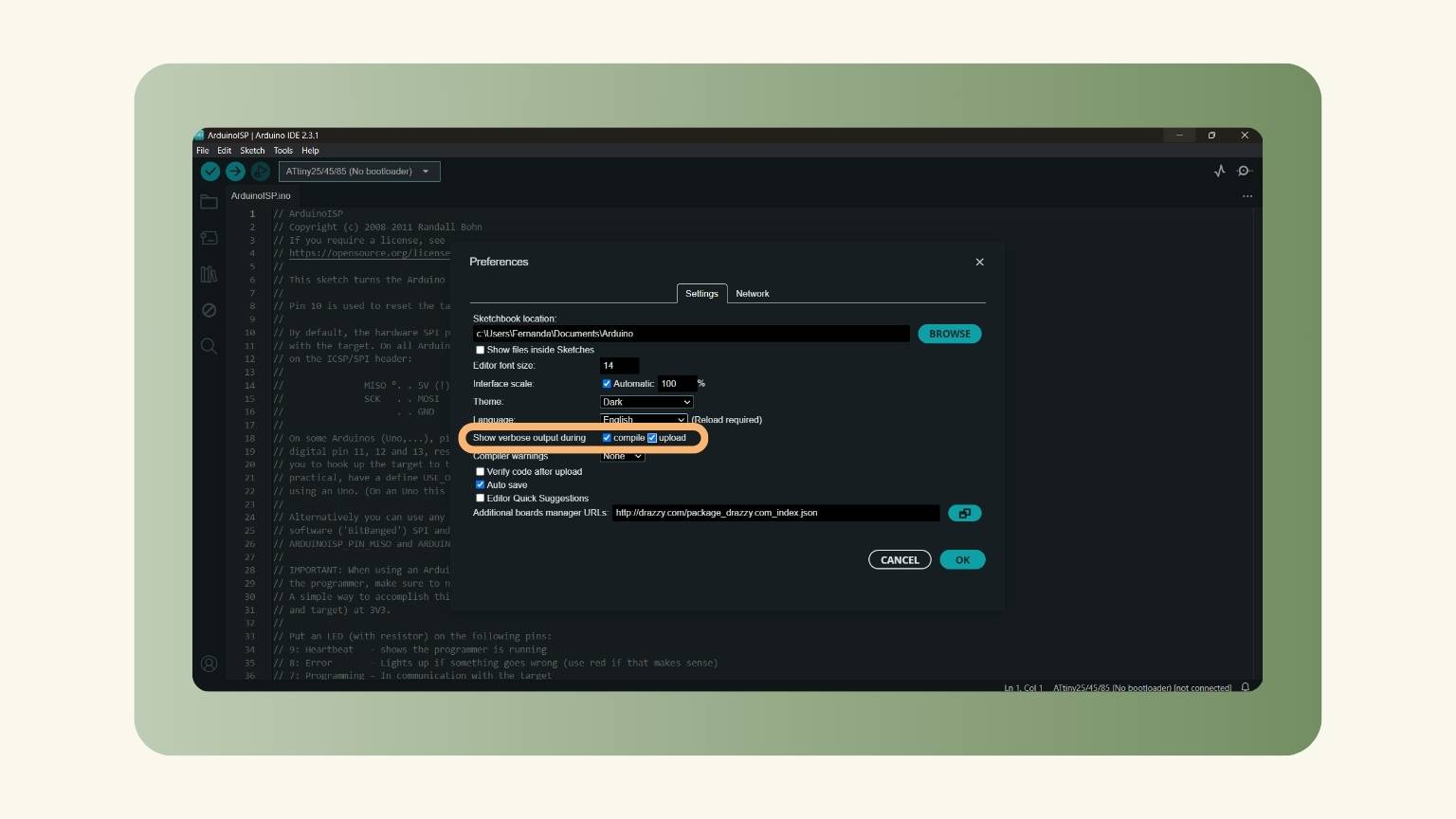
- Then I opened the ‘Preferences’ menu to select the two options in the ‘Show verbose output during’.
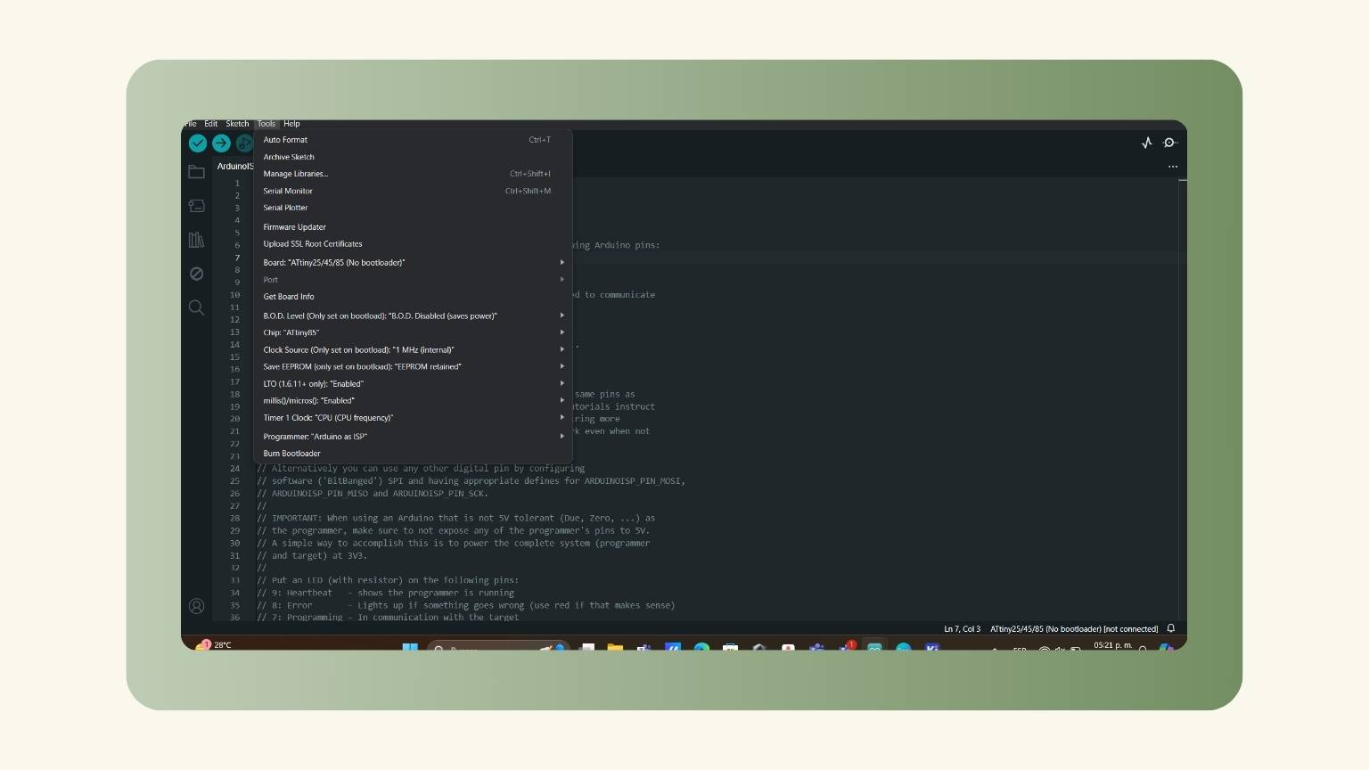
- In the ‘Tools’ menu, I checked that the options were good.
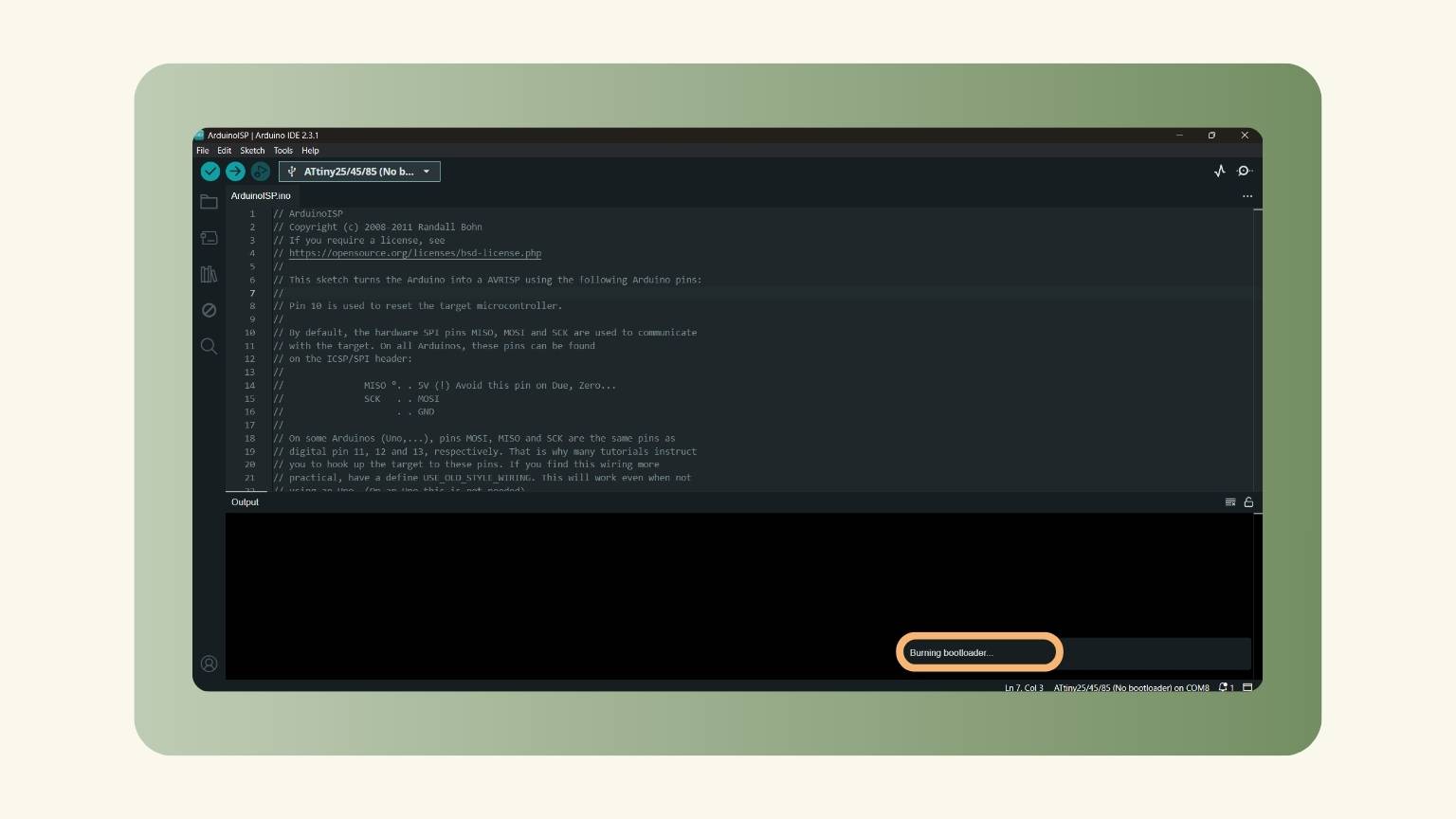
- I selected the ‘Burn Bootloader’.
- The action was executed.
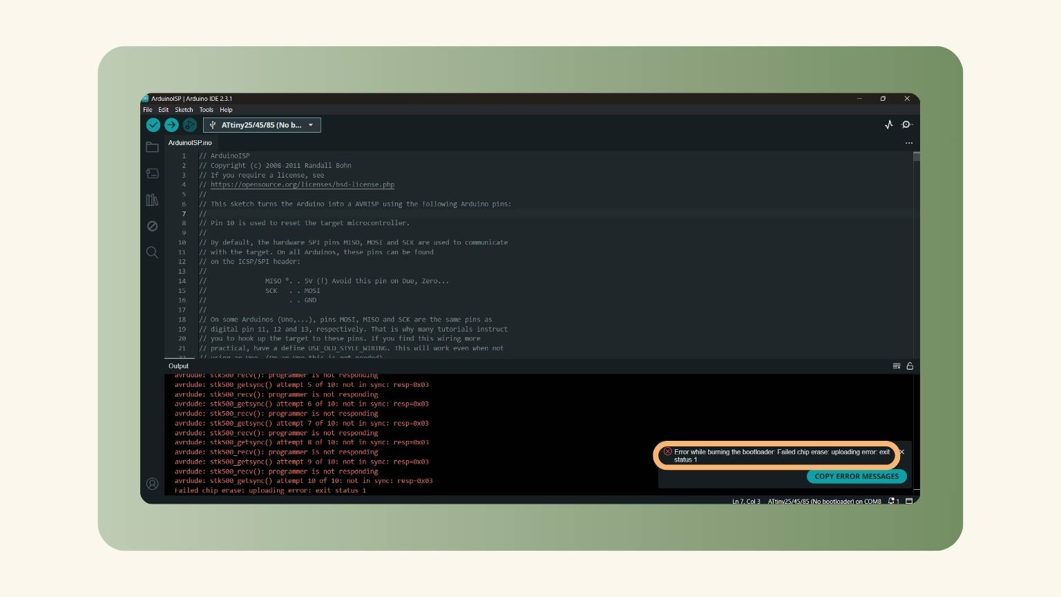
- But the actions failed.
- The mistake was in the selection of the chip. I selected the 'ATtiny85', and it must have been the ‘ATtiny45’.
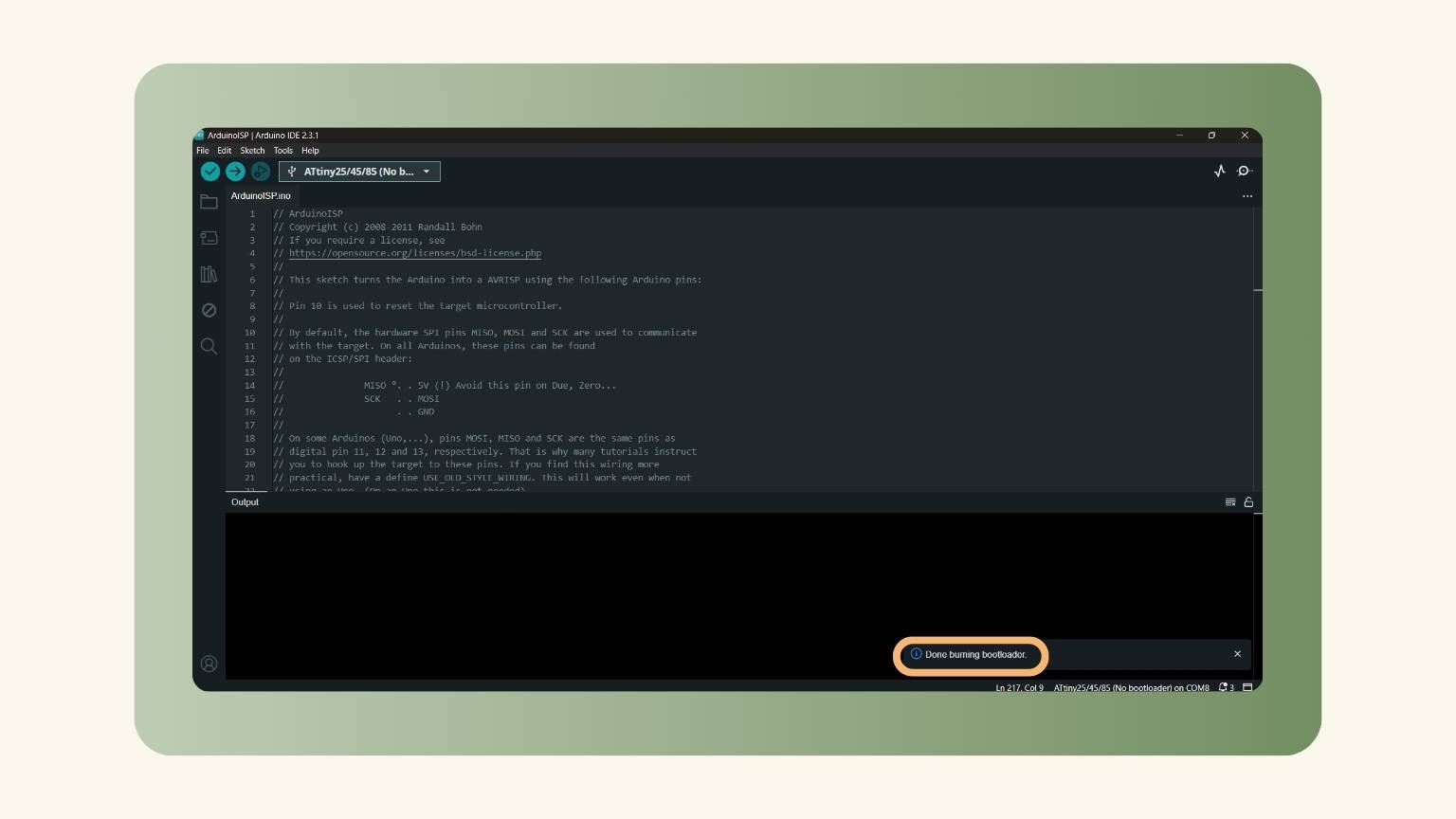
- I corrected the mistake, and the burning bootloader was done.
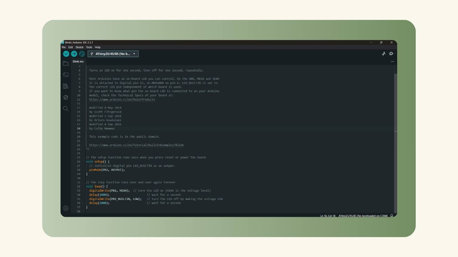
- Then I used the ‘ Blink Example’ to check the function of the PCB. And I changed the number of the pin.
- I verified the characteristics in the 'Tools’ menu.
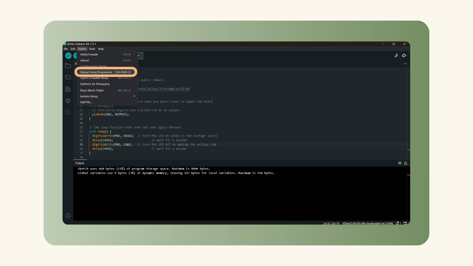
- I uploaded the file with the ‘Upload Using Programmer’ option in the ‘Sketch’ menu.
- The result wasn’t as expected because the track of my LED is the same as a pin. Both were connected to the PB4 pin of the ATtiny.
- So, in this example, the LED that lit up was the one on the Arduino, the one on the pin that was connected.
- Then I made a code to use the Neopixels on my PCB.
- This was the code:
- And this is the result:
NEOPIXELS
Conclusion
In one week, I accomplished a complex task. Despite the chaos, I persevered and hope to continue doing so.