4. Electronics Production
During this week, we had the opportunity to design and test a microcontroller development board. Originally, we planned to base it on the quentorres design. However, we encountered a challenge when we discovered that one of the components, the SWD, was not readily available in Mexico and cost 5 US$ dollars. As a result, we had to create a modified version of the board that better suited our needs.
but for that I had to understand more about the subject...
What is a circuit?
Did you know that a circuit is basically an electronic network that has at least one closed path? It's made up of a bunch of different components like resistors, inductors, capacitors, sources, switches, and semiconductors.
Basic components:
- LED.
- Capacitador.
- Regulator
- Resistor
- Diode
What is a PCB?
A printed circuit board (PCB) is made up of an electrically insulating base on which conducting metal tracks are etched to make electrical connections for electronic components positioned on the top and, in some cases, bottom.
PCB Fabrication
PCBs are made from drawn lines instead of using wires.
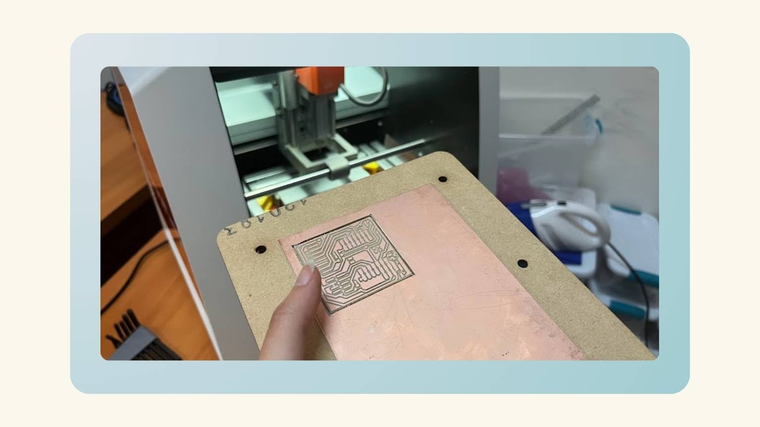
The manufacturing process involves two steps: first, the copper is engraved and the circuit is drawn with a milling machine, and second, the PCB is cut by drilling and contouring with the same machine.
What machine will we use?
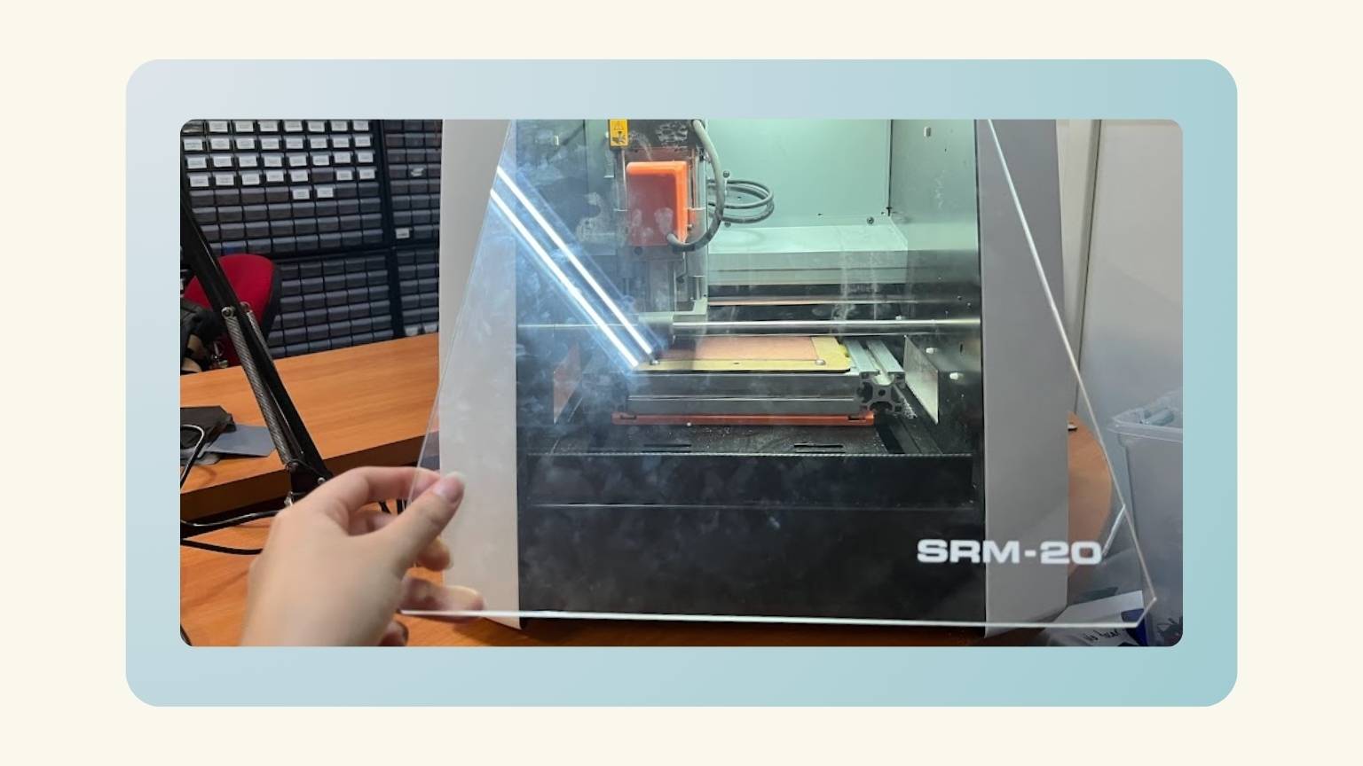
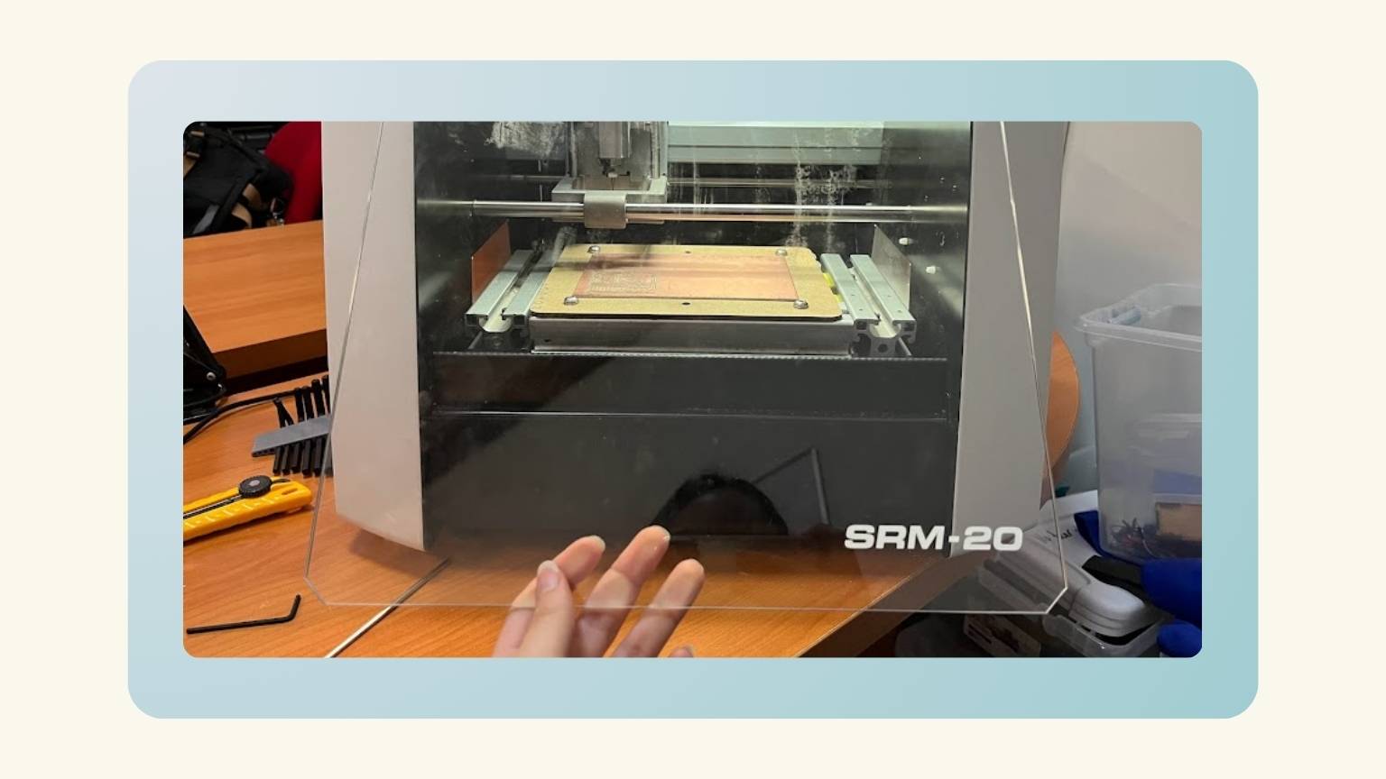
ROLAND SRM-20
This machine can cut a broad range of materials, including chemical wood, acrylic, and ABS. It also supports a wide variety of accuracy settings, from prototype to product design. Furthermore, its tiny size and fully enclosed design allow you to cut with greater safety and confidence.
What tools will we use?
V-Cutter, allows for better engraving for its fine tip.
Flute end Mill, for drilling and plate cutting.
Parameters importants
When PCB milling, there are only a few aspects that we can control and test. These include:
- Drill Hole Size: This parameter is important because it affects the ability to precisely put vias and mount components. The dimensions must be accurate to ensure that the components fit correctly without tension or misalignment. Incorrect hole diameters can cause poor electrical connections or even damage to components during installation
- Substrate: The material used for the substrate influences the PCB's thermal, electrical, and mechanical qualities. Different materials have varying levels of conductivity, durability, and heat resistance, which impact the effectiveness of the PCB in certain applications. For example, FR4 is often used because of its low cost/performance ratio, although more specialized applications may demand materials like Rogers due to their higher high frequency performance.
- Minimum Clearance: This value specifies the shortest possible distance between any two conducting elements (e.g., traces, pads) on the PCB. Ensuring proper clearance is critical to avoiding electrical shorts and ensuring dependable functioning. It is impacted by the voltage levels that the board is exposed to, with higher voltages necessitating larger clearances.
- Minimum trace width: This specifies the smallest width for each conductive trace on the PCB. It is critical to verify that traces can handle the needed current without overheating or breaking. The minimum trace width is determined by the maximum current that the trace must carry, while taking into account the material's conductivity and the PCB's operating temperature.
- Number of layers: : This value defines how many conductive layers the PCB contains. Multilayer. Multilayer boards are used to enhance component density and routing complexity while maintaining board size. The number of layers influences the PCB's electrical performance, manufacturing complexity, and cost. It is critical to weigh the requirement for additional layers against the economic implications and production capability.
What are mods?
Mods is a program that allows me to extract G-codes or machine codes from images, vectors or 3d models.
Advantages:
- For all machines.
- Open source.
- Web server, so that on any computer you can use.
More information
This is a summary of the key aspects to consider in electronic production. For more information, please refer to the Fab Lab Puebla group page.
What did I do with all this information?
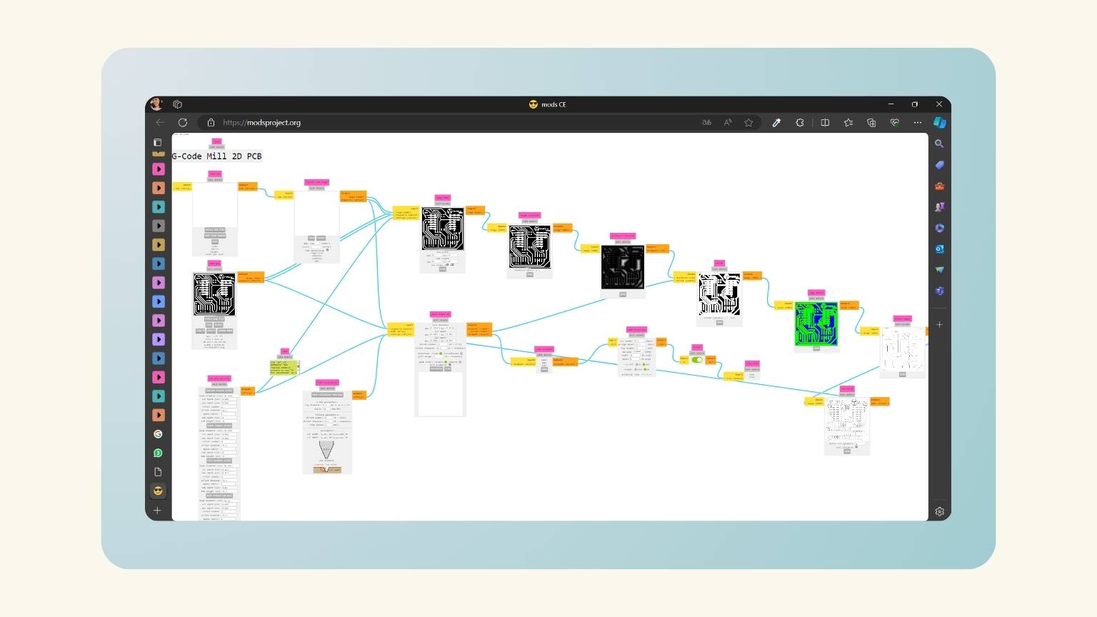
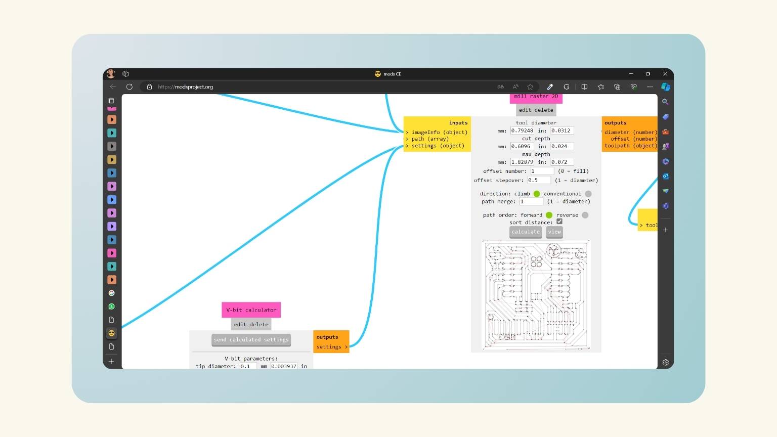
How does it work MODS?
First, how do we transfer the files to the machine?
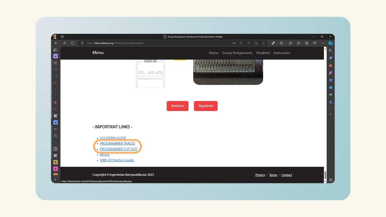
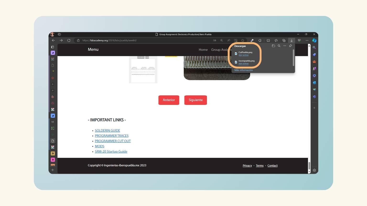
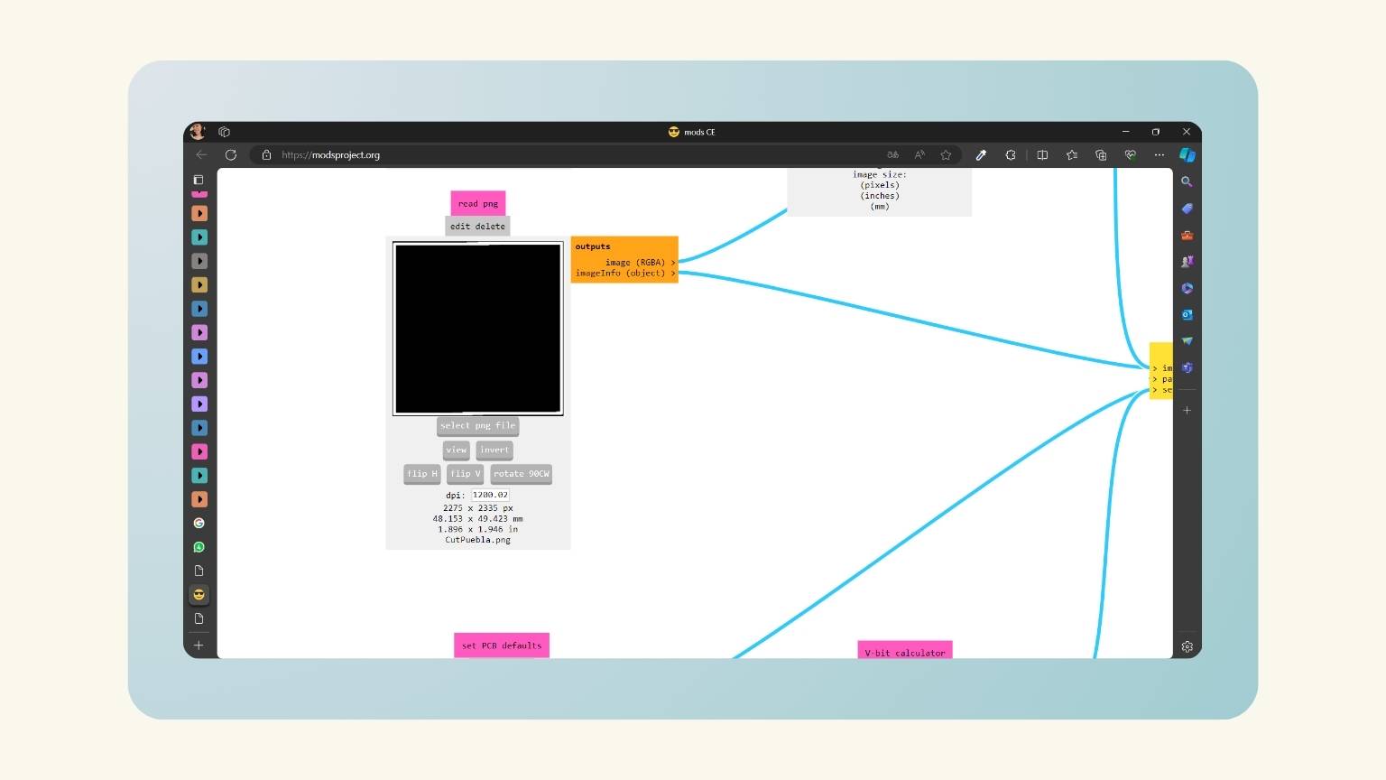
- I searched the png images that they provided us on the FabLab Puebla website.
- I downloaded two png images.
- The images have a size of 4.8.
- They are black and white.
- Note: Don’t modify the image because the image can scale. And if we change the scale, the components won’t fit.
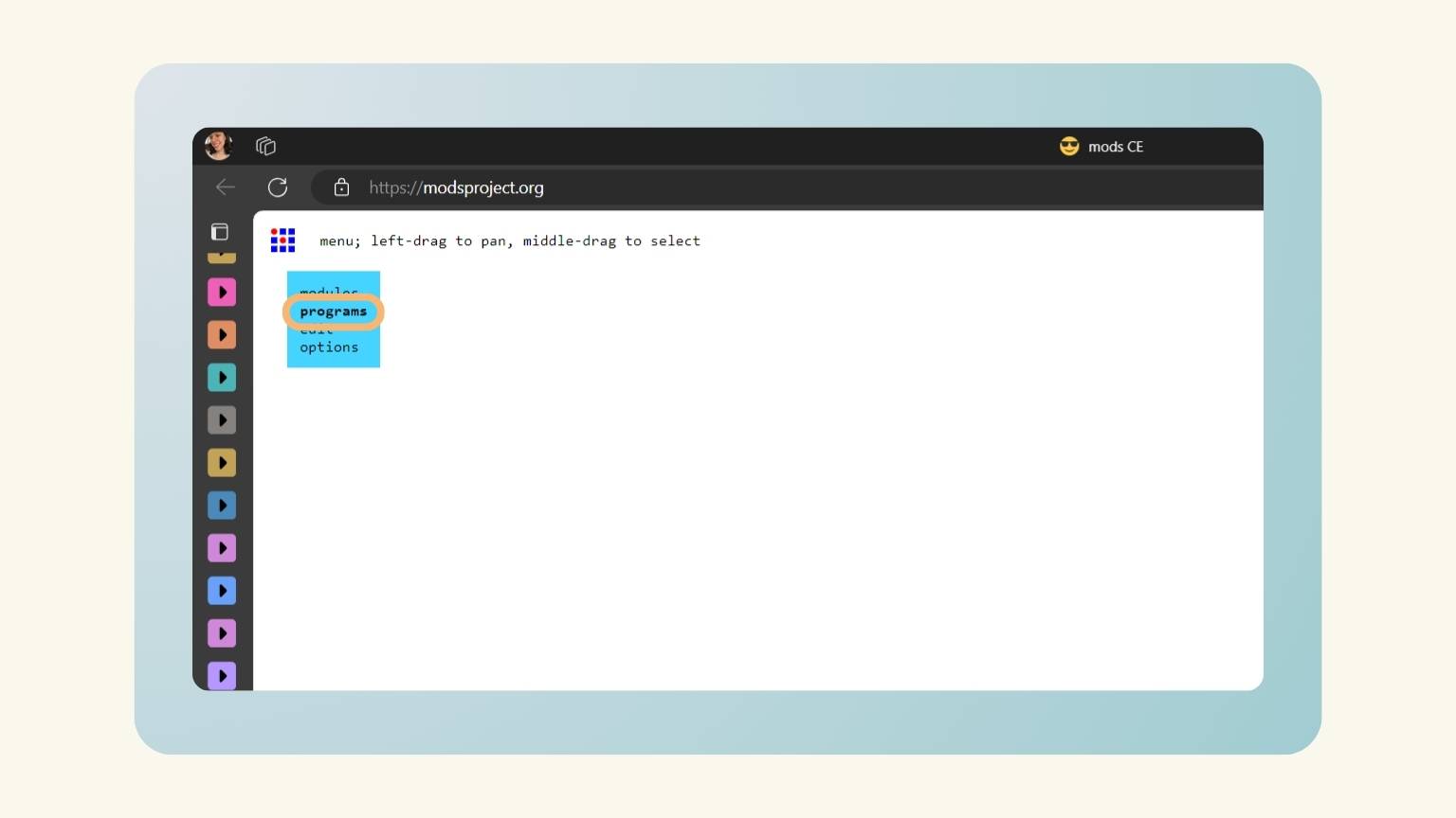
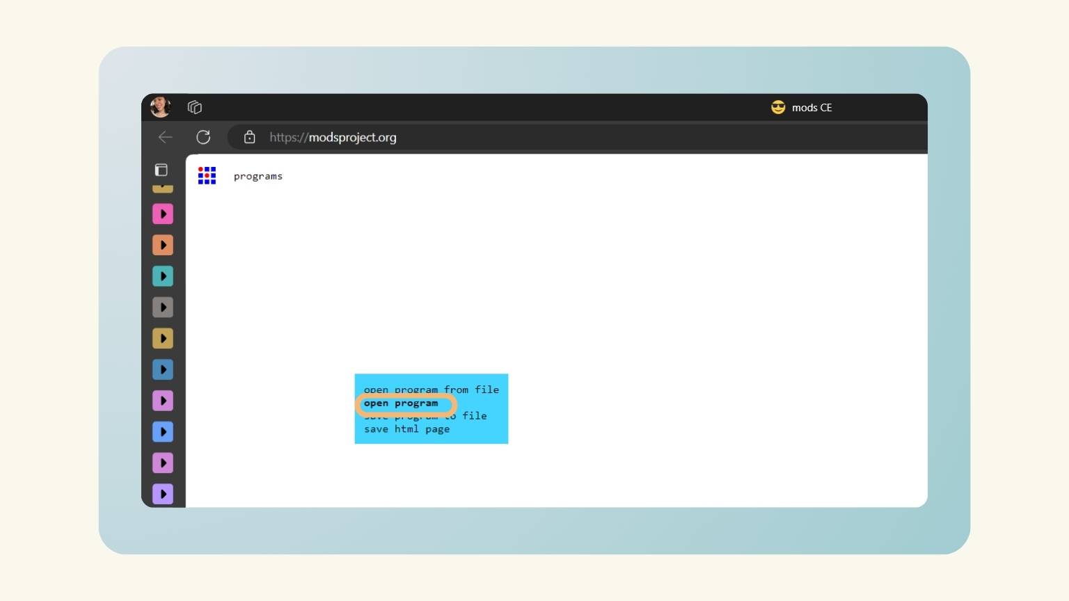
- I opened the MODS web server.
- I right clicked on ‘Programs’
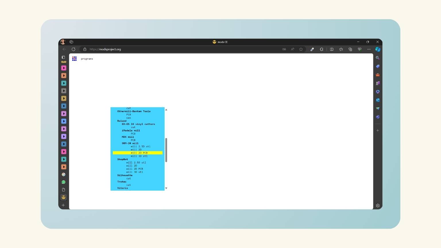
- Next in ‘Open program’
- I searched the program of the SRM-20 mill machine and selected the ‘mill 2D PCB’.
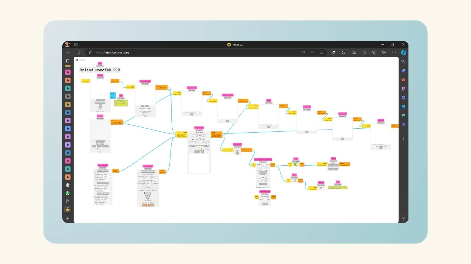
- All the blocks to be worked on are displayed to obtain the corresponding files.
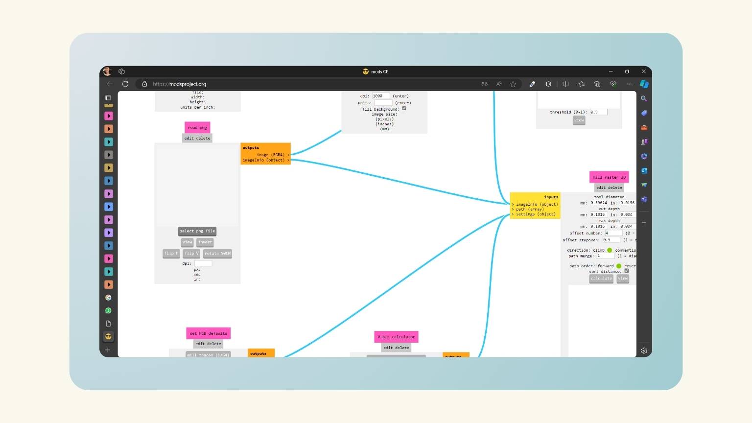
- The first block that I modified is the 'read png’ block for selecting a png file.
- I saw that the image was uploaded to the server.
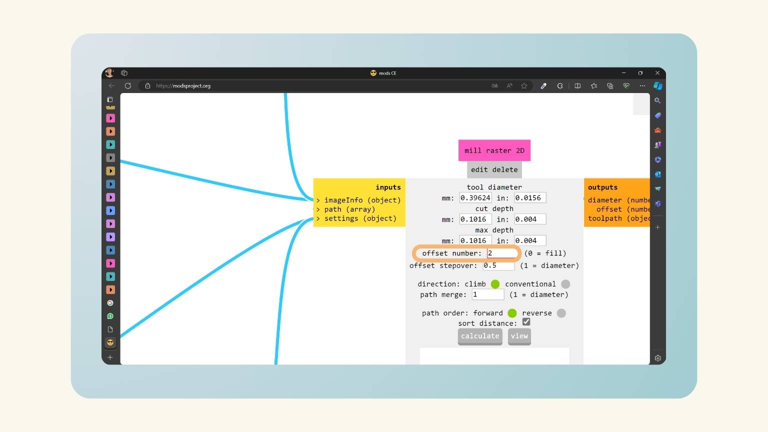
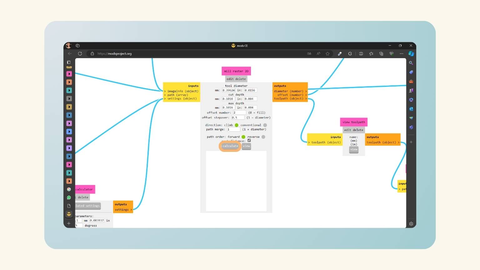
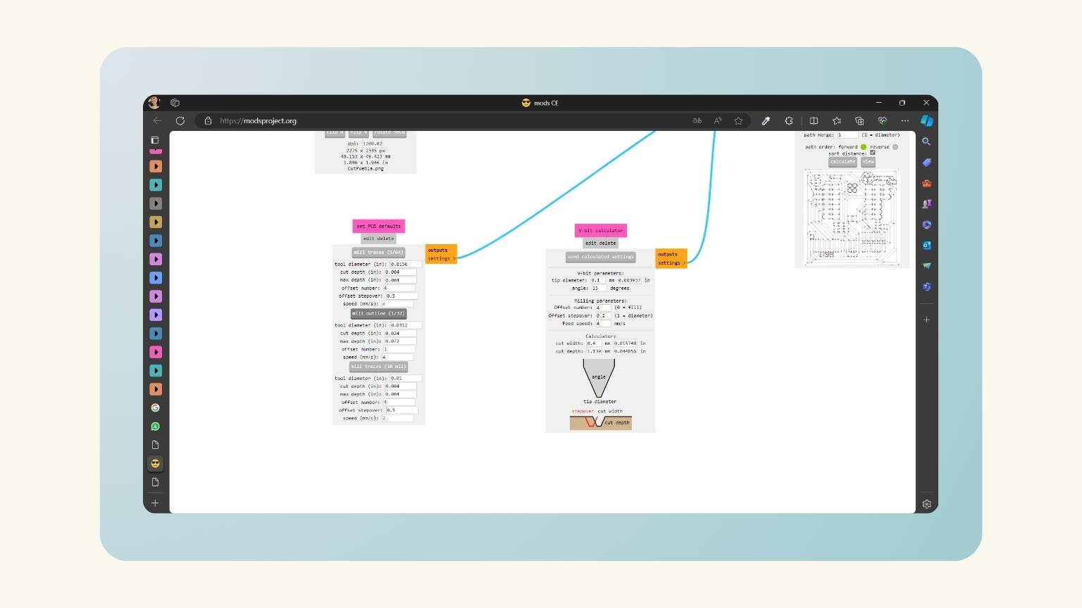
- I moved to the ‘mill raster 2D’ block. And I changed the ‘offset number’ to two.
- This determines the number of times it will be passed to be cut. It was engraving, so this number is fine to have this result.
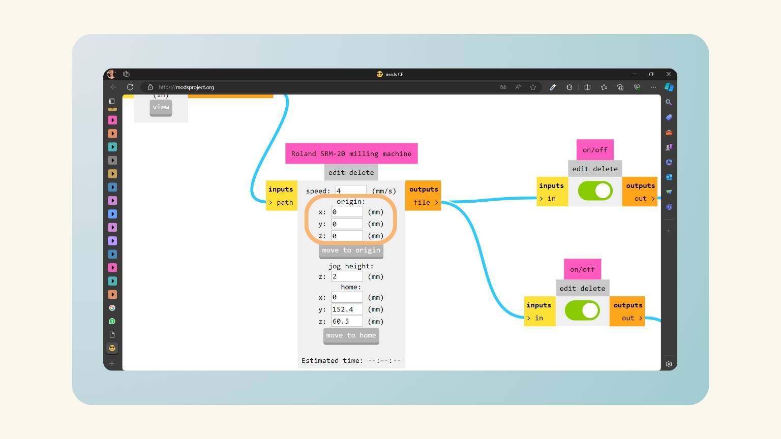
- Then, I went to the ‘Roland SRM-2D milling machine’ block, and I modified the origin of the machine. For this, I changed the numbers on the axes x, y, and z.
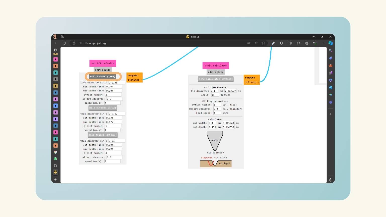
- After, I went to ‘set PCB defaults’ and pressed on ‘mill traces (1/64)’ to make the changes in the machine parameters.
- I moved to the ‘mill raster SD’ to see if the changes were realized. And then I pressed ‘calculate’.
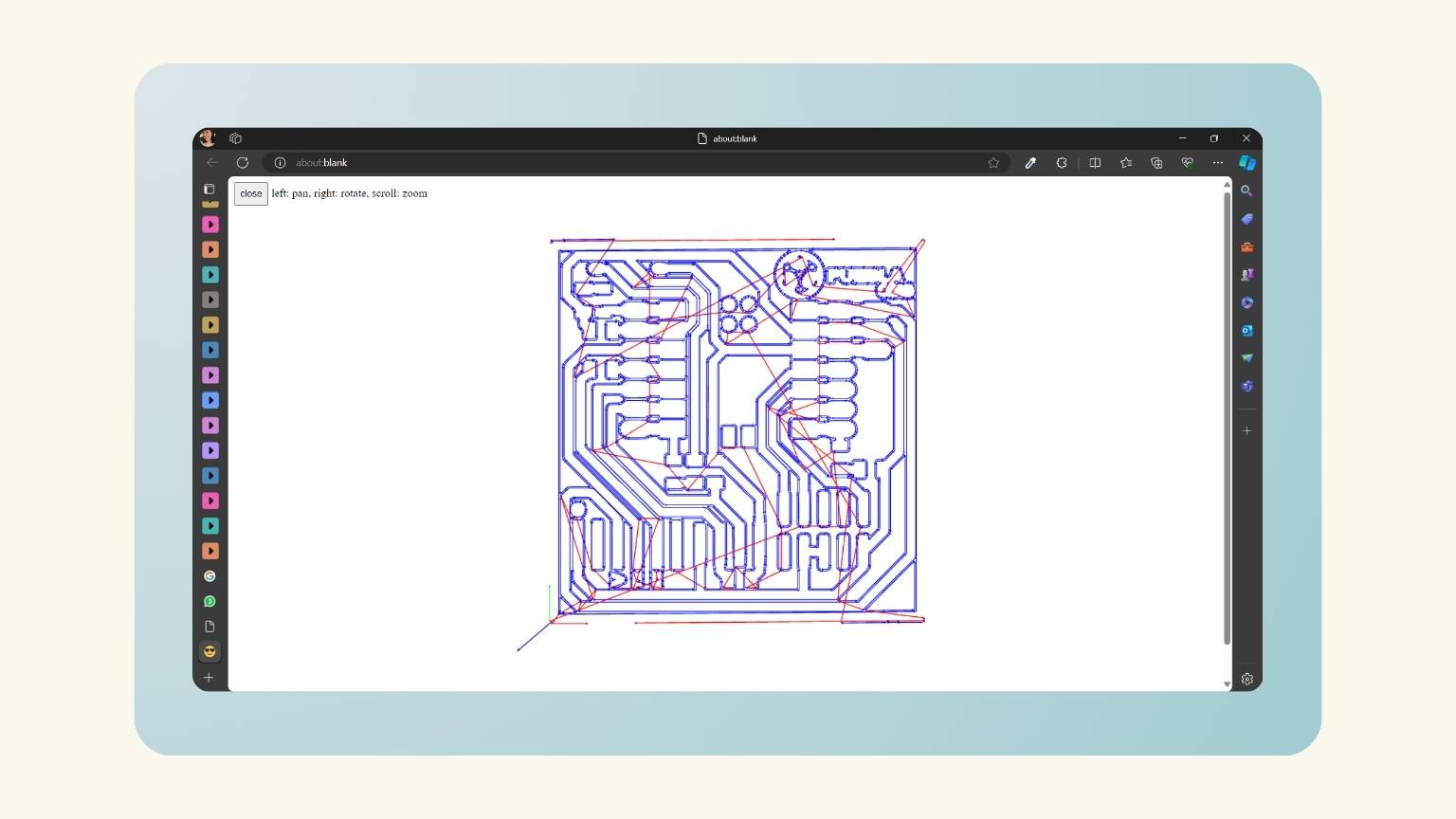
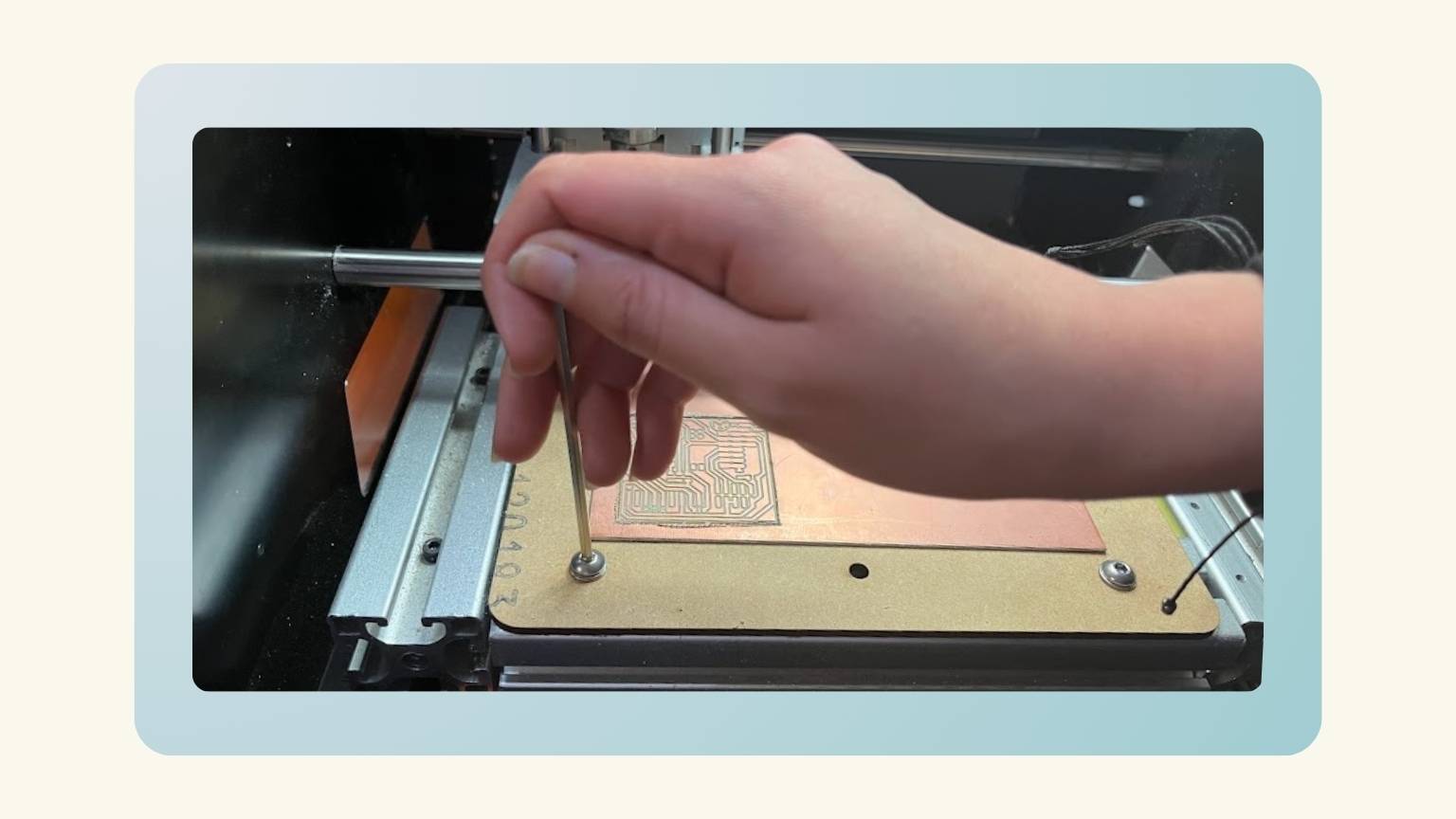
- From my image, what to do is trace the route that the machine will follow for the engraving.
- And I saw a preview. In addition, in my downloads, I found an archive ‘.png.rtl’; this is the file that I opened on the machine.
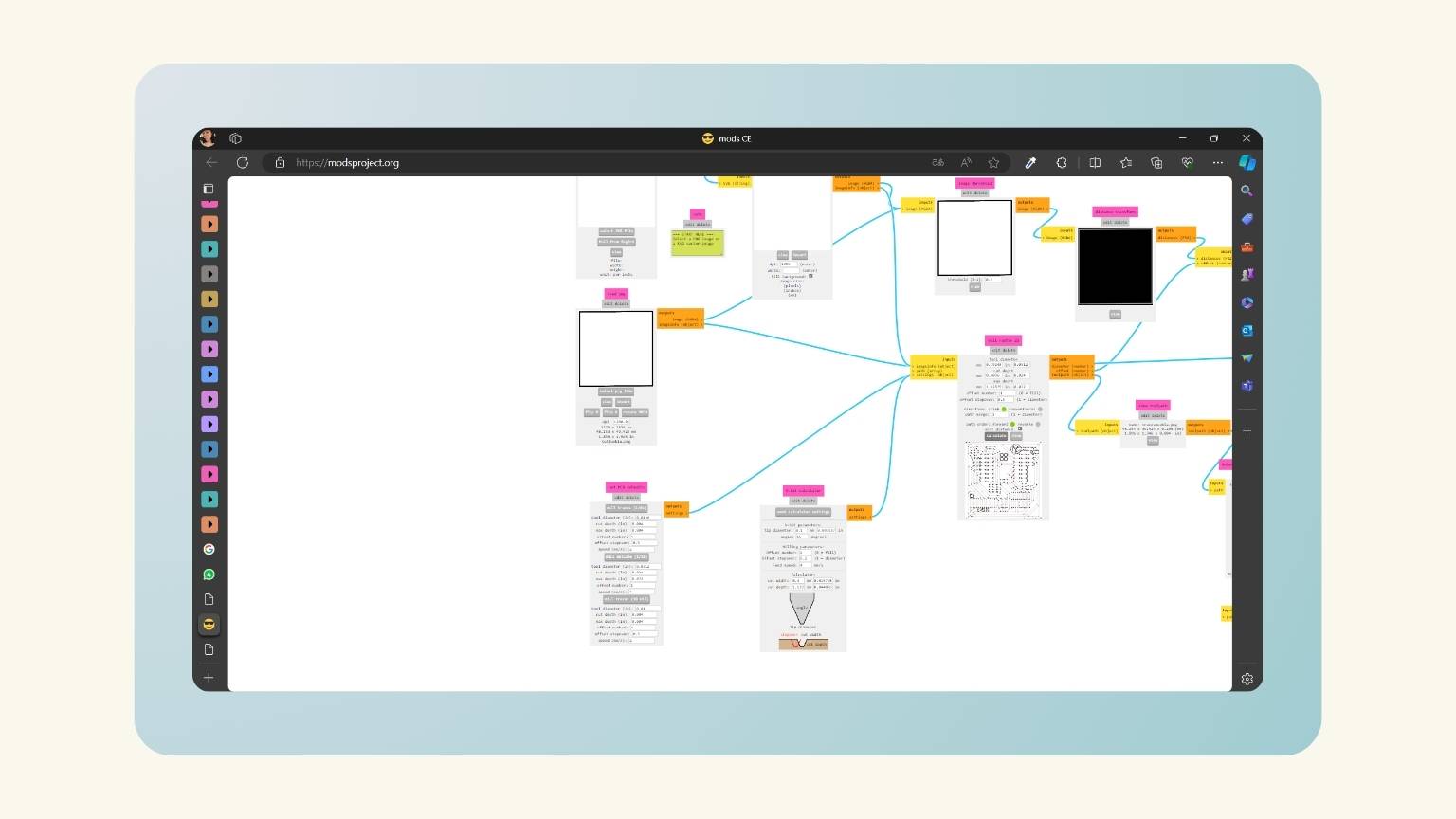
- Next, I did the same steps with the image of the cut. Starting by selecting the cut image of my files.
- I moved to the ‘set PCB defaults’ block and pressed ‘mill outline’.
- Then, I went to the ‘mill raster 2D’ block and changed the ‘offset number’ to one.
- And I pressed calculate to see the preview of the cut and downloaded the file for the machine.
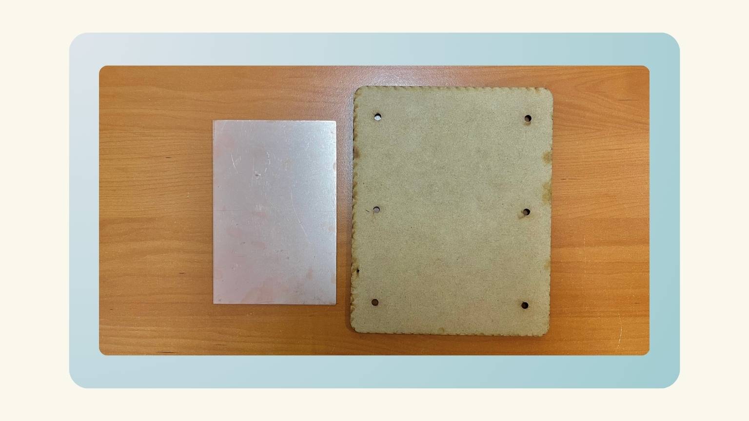
Things I should have before cutting
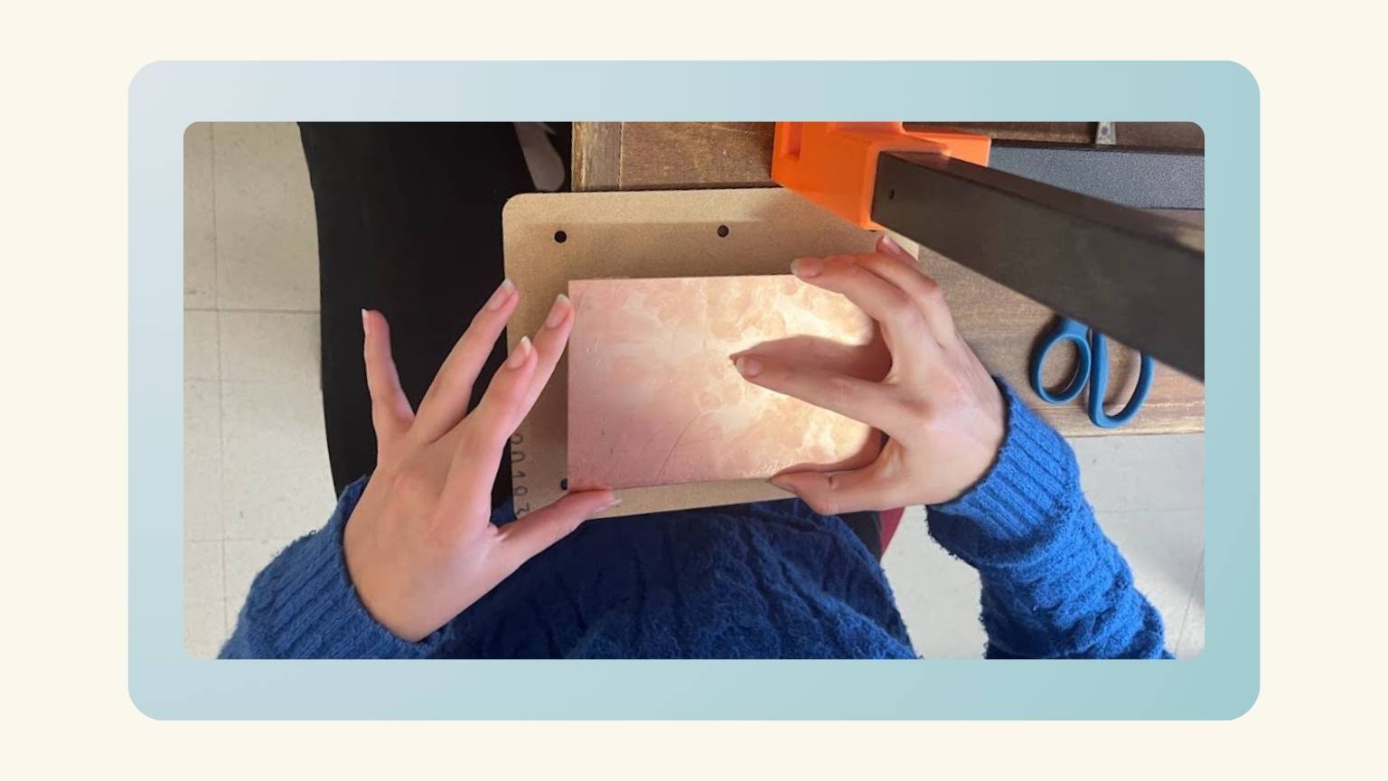
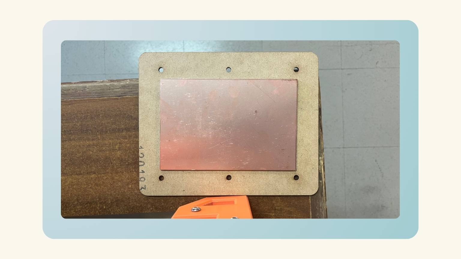
- First, I cut in the laser a sacrificial piece to put the copper plate on top to avoid damaging the machine table when cutting.
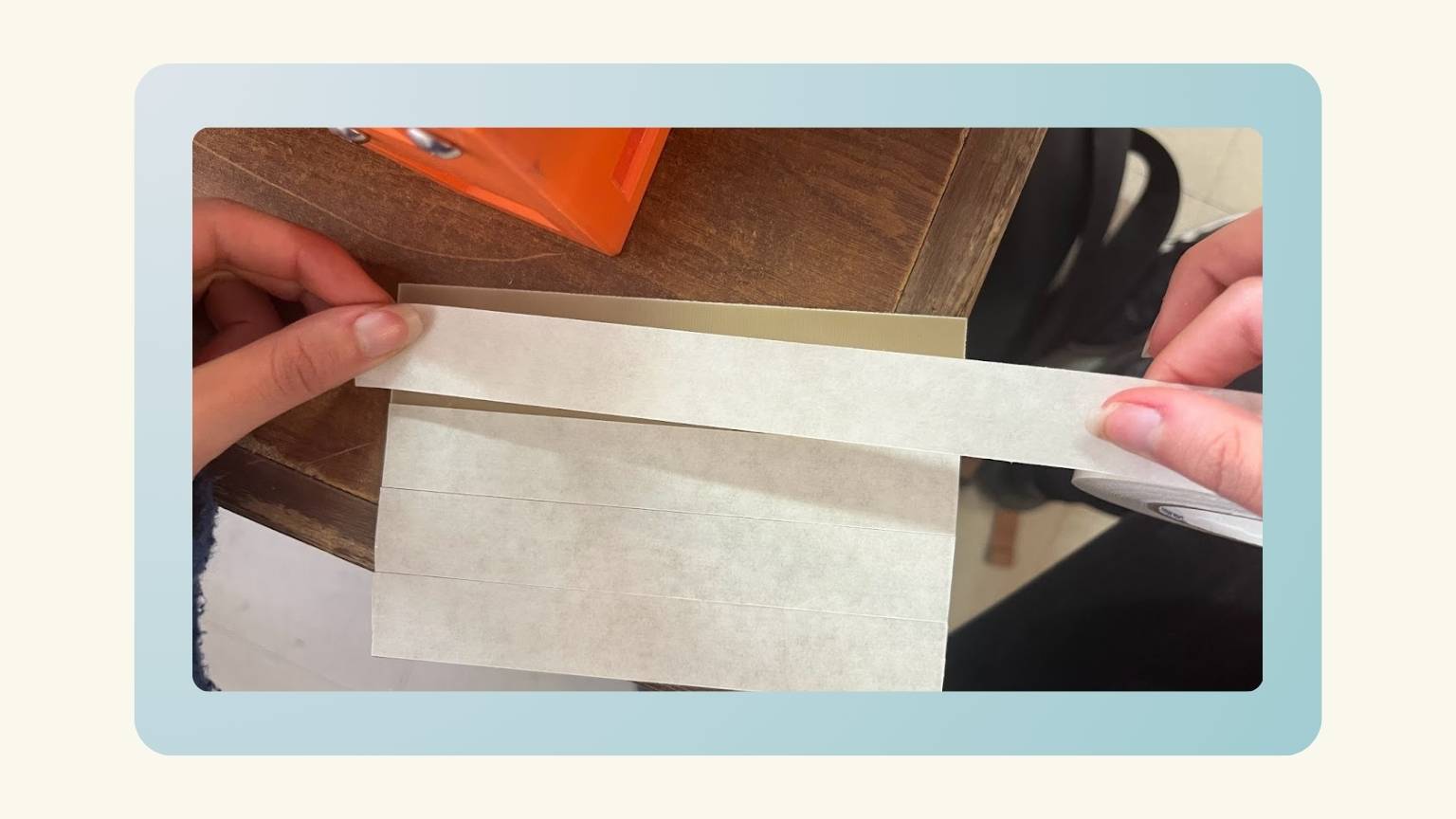
- Then, I put paper insulating tape on the base of the copper plate to paste it on the sacrificial piece.
- Note:Use paper insulating tape because if you use another one, you generate relief.
- When I put the tape in all the base and removed the glue protector, I pasted the cooper plate on the sacrificial piece.
- And I have the material to cut on the machine.
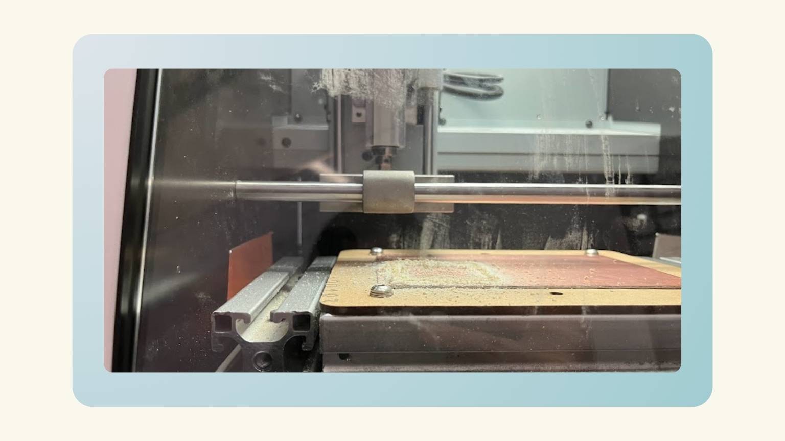
Now, how can I use the machine?
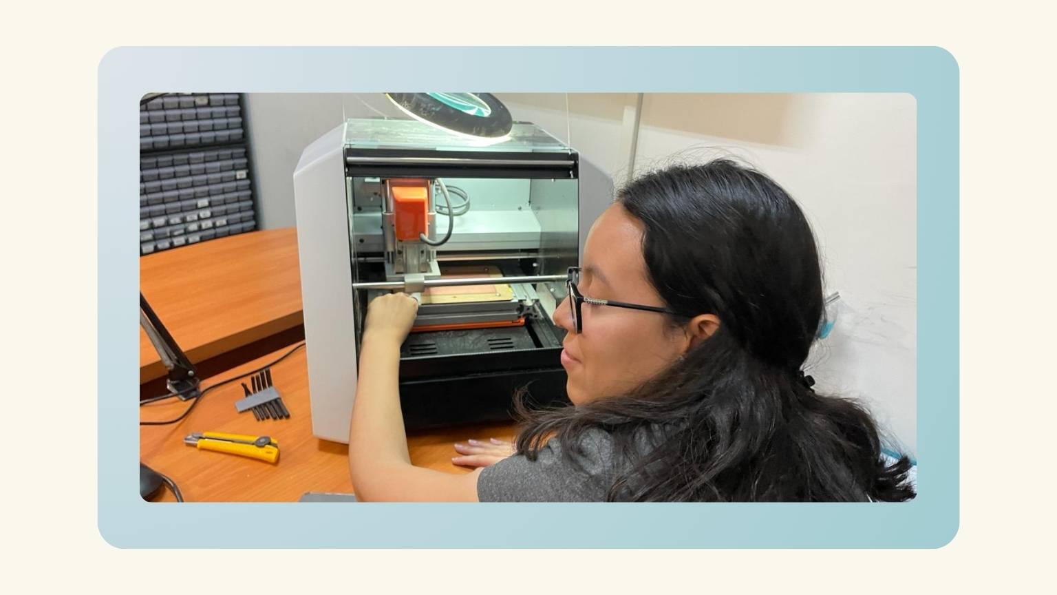
- I put my sacrificial layer with the cooper plate and my card in the base of the machine.
- To this I used screws to fix it. And I used a screwdriver to tighten the screws.
- I placed the tool, a 15 degree V-bit, to make the engraving.
- To do this, I used a wrench to tighten the tool.
- Note:Make sure that only the conical part of the tool protrudes.
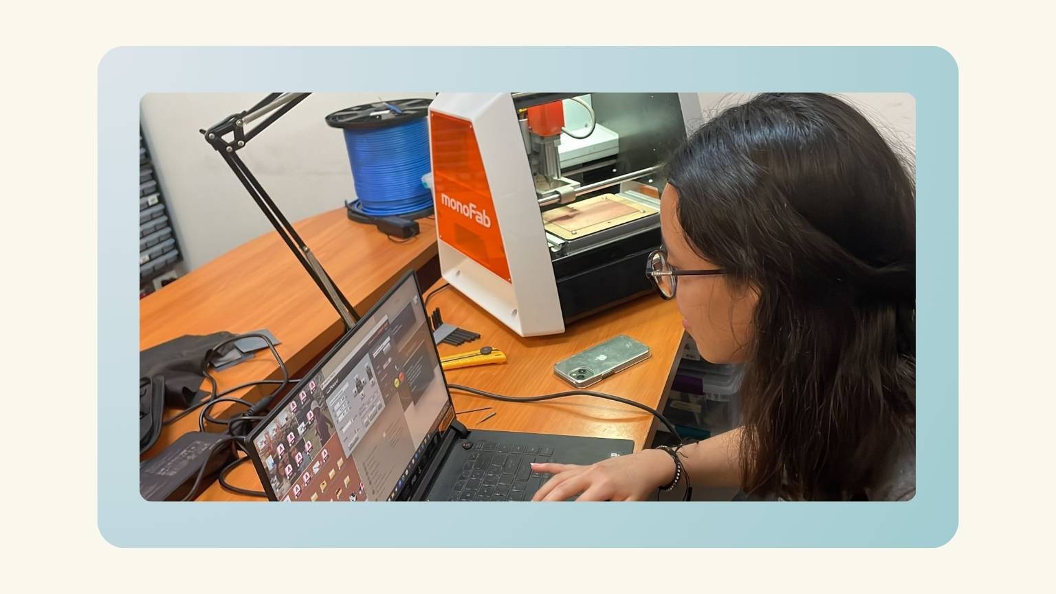
- I connected the machine to my computer.
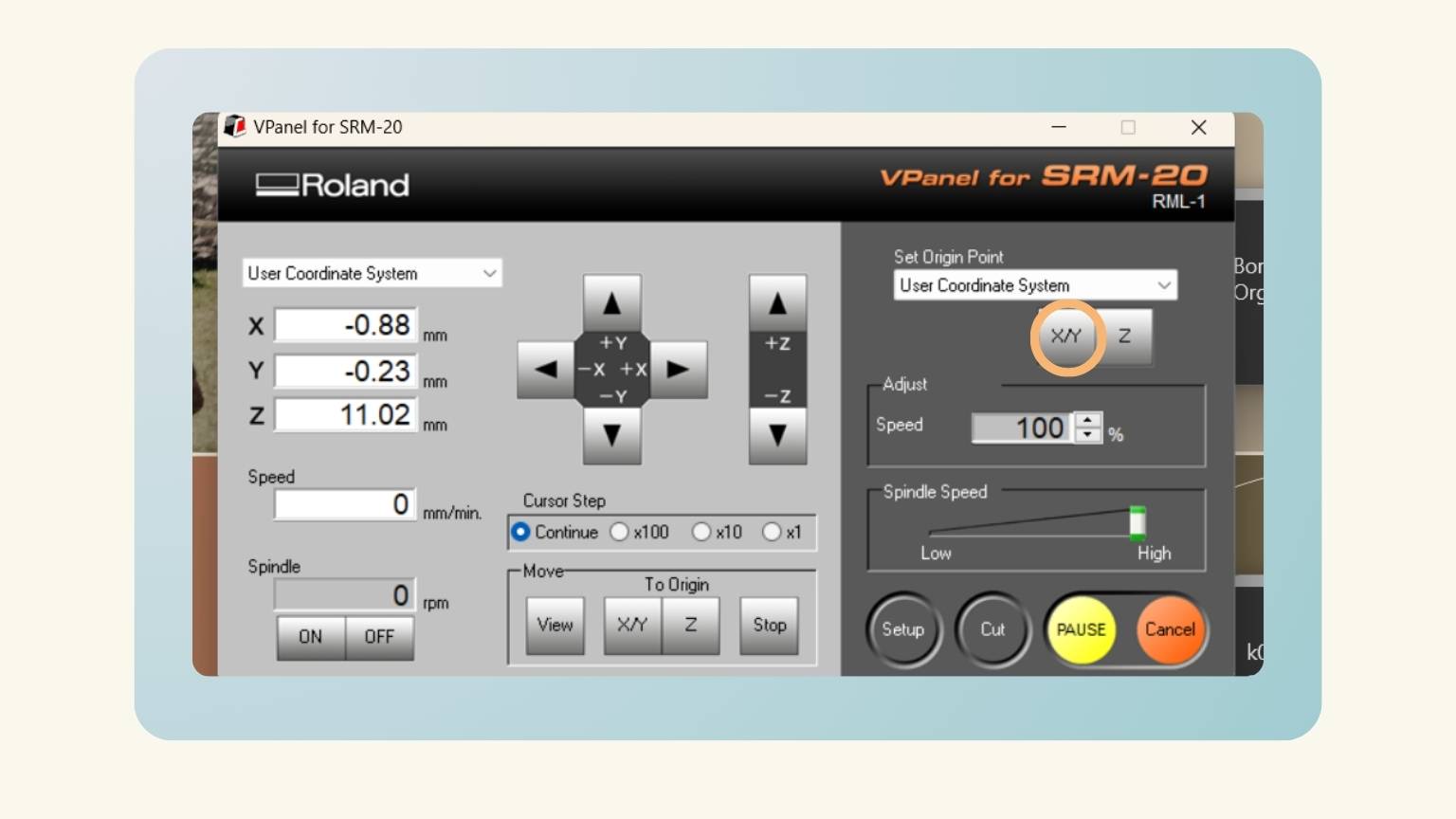
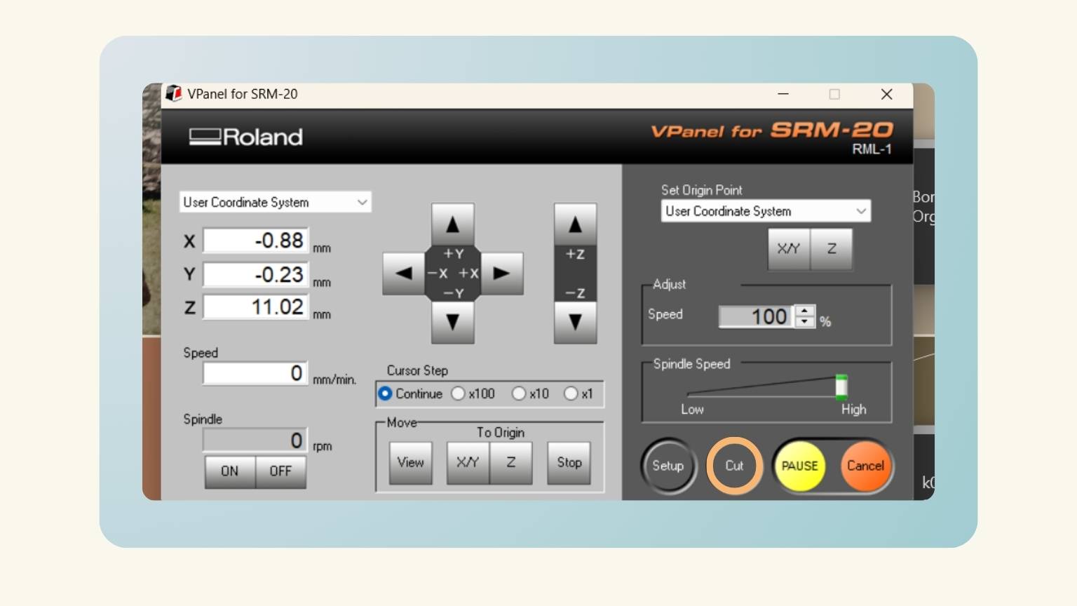
- I open the ‘VPanel for SRM-20’
- Because the operation of this machine is performed on the screen of a computer using [VPanel].
- P.S. As you can see in my wallpaper, I’m still in January hahaha… the Fab Academy gradually takes away your sense of time.
- So, I saw the control panel of the machine.
- View: Moves the spindle head to the center and moves the table to the very front.
- XY / Z: Moves the cutting tool to the XY origin point.
- Stop: Stops the cutting tool at that point when it is moving.
- Ser up: Sets the cutting machine's operating conditions and the correction values for the axes
- Cut: Configures cutting settings.
- Pause: Pauses and resumes cutting.
- Cancel: Cancels cutting.
- First, I moved the X/Y axis to the lower left of the material.
- And I pressed the ‘X/Y’ bottom to change the origin of this axis’s.
- Then, I moved the Z axis. To do this, I used a piece of paper to make sure I put the axis at the correct height.
- For this special axis, I used a paper to define the distance between the tool and the material. I did this by placing the paper on the material and lowering the tool a little at a time until the point where friction is generated and the paper gets stuck.
- Note: In this axis, before we did the paper check, we had to turn on the spindle and lower the z-axis, giving only one click to selecting ‘x10’ in the cursor step.
- I save the origin of the axis by pressing ‘Z’.
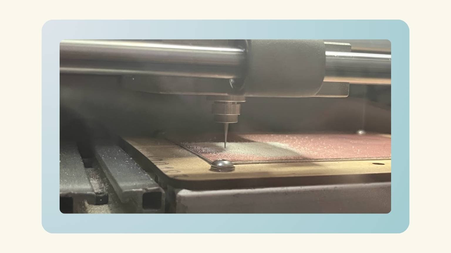
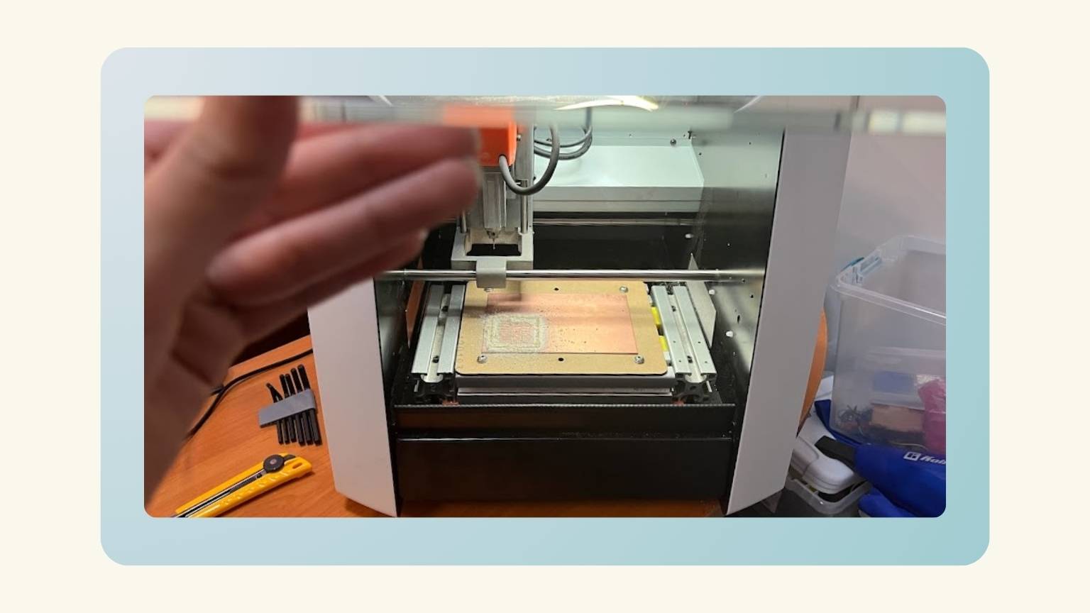
- When I defined the axis of origin, I closed the door of the machine.
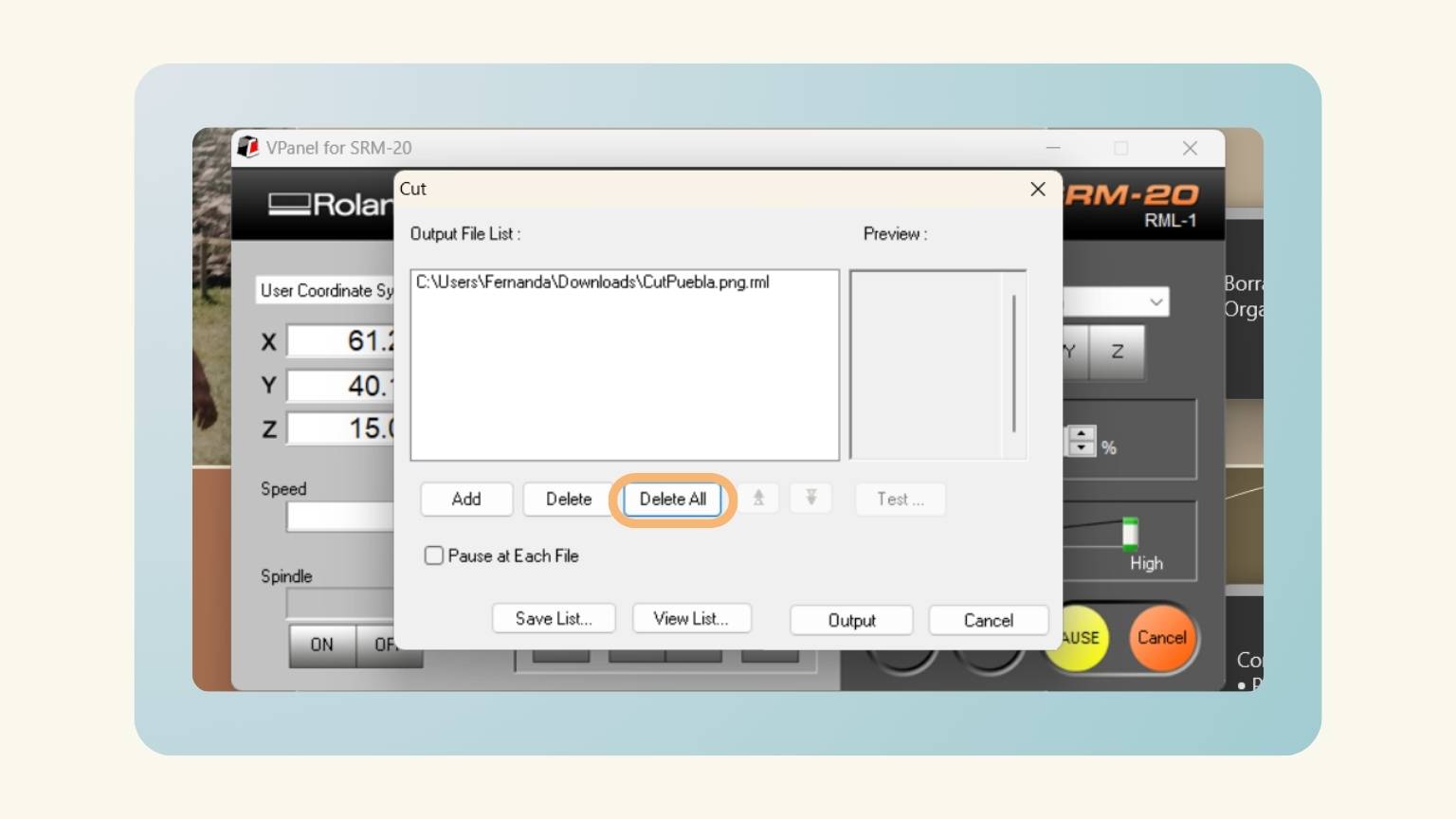
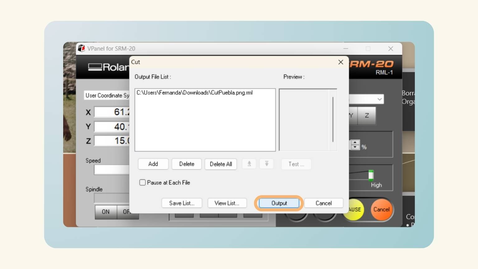
- Then, I pressed the 'Cut' button at the bottom of the panel.
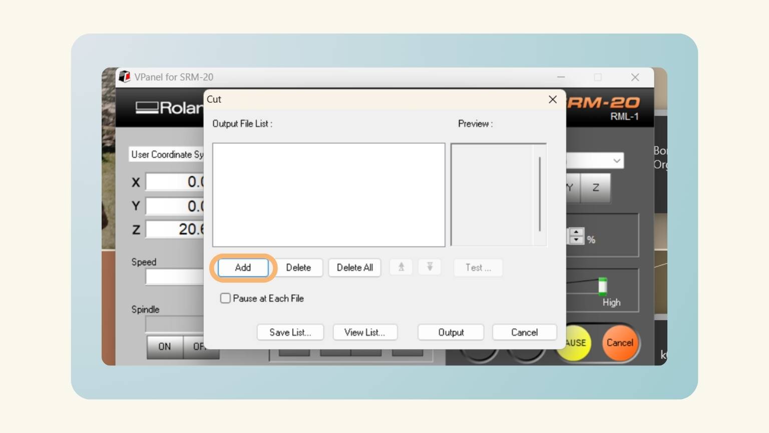
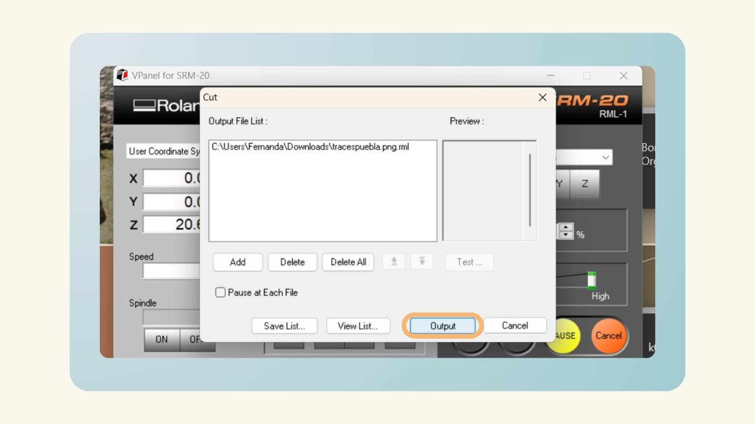
- I added the file to be engraved.
- I pressed ‘Outpt’ to send the file to be engraved.
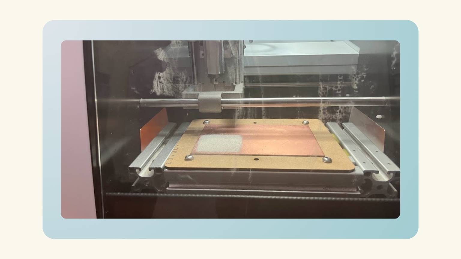
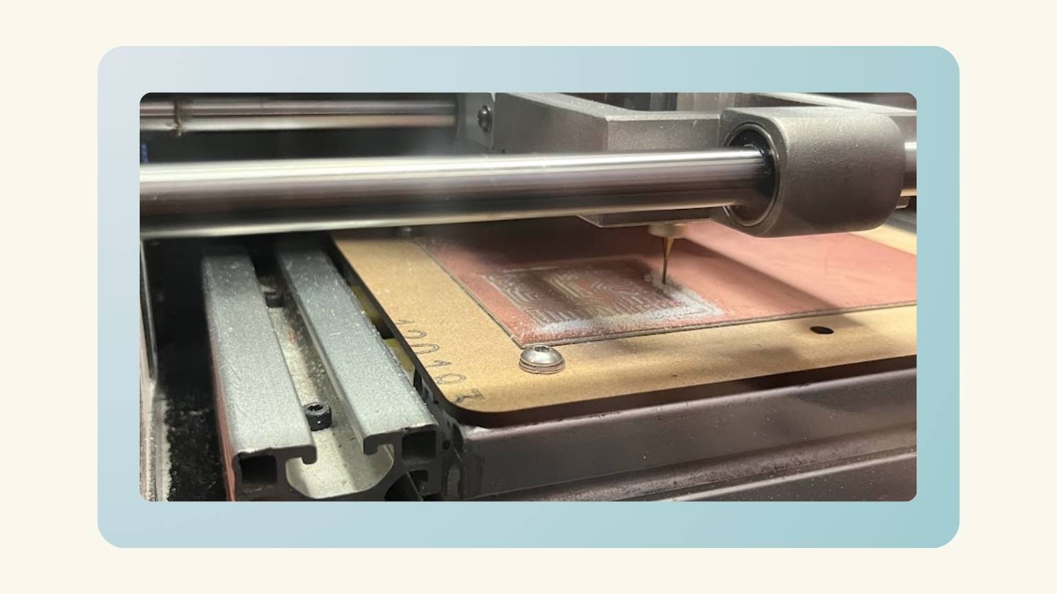
- And the machine started to engrave.
- When the engraving was finished, the spindle went to the origin point.
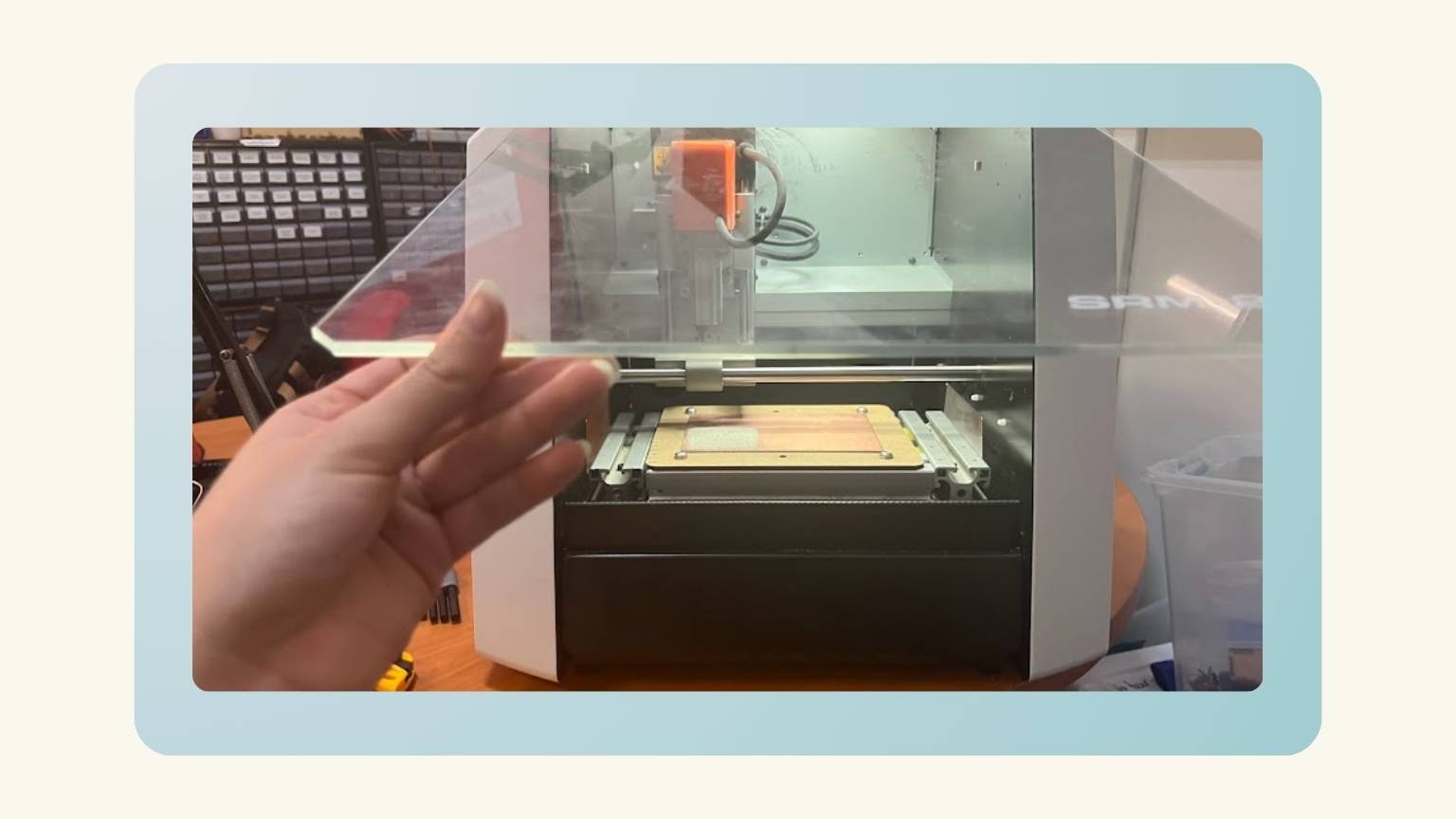
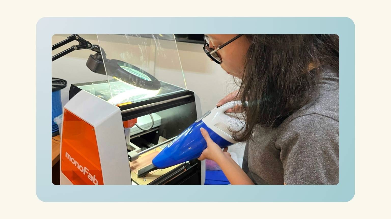
- I opened the door of the machine.
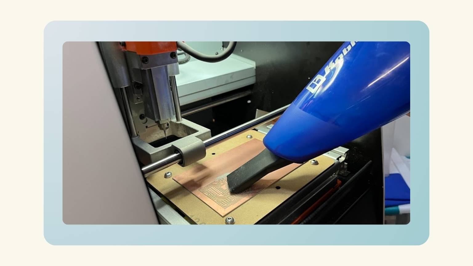
- I used a hand vacuum cleaner to remove the dust produced by the engraving.
- I removed the tool that the machine had because it wasn’t the right one.
- So, I changed the previous tool for a 0.8 mm diameter two-flute end Mill this to do the cut.
- For this, I used a wrench to tighten the tool.
- Note:Make sure that the conic part protrudes.
- I maintained the ‘X/Y’ origin and only changed the ‘Z axis’ because the tool was different and it was necessary to reconfigure that axis due to the height of the tool.
- So, I changed the previous tool for a 0.8 mm diameter two-flute end Mill this to do the cut.
- To change this axis, I used the method of the paper, which I described in step 9.
- I save the new origin of the axis by pressing ‘Z’.
- Then, I closed the door of the machine.
- I pressed the ‘Cut’ button to delete the previous file that I added.
- I added the new file of cut.
- And I pressed ‘Output’ for the machine to execute the cut.
- The machine started the cut.
- The machine finished the cut.
- I opened the door to withdraw the material.
- I used a hand vacuum cleaner to remove the dust produced by the cut.
- I removed the screws fixing the material with the help of a screwdriver.
- Finally, I had my card burned and cut.
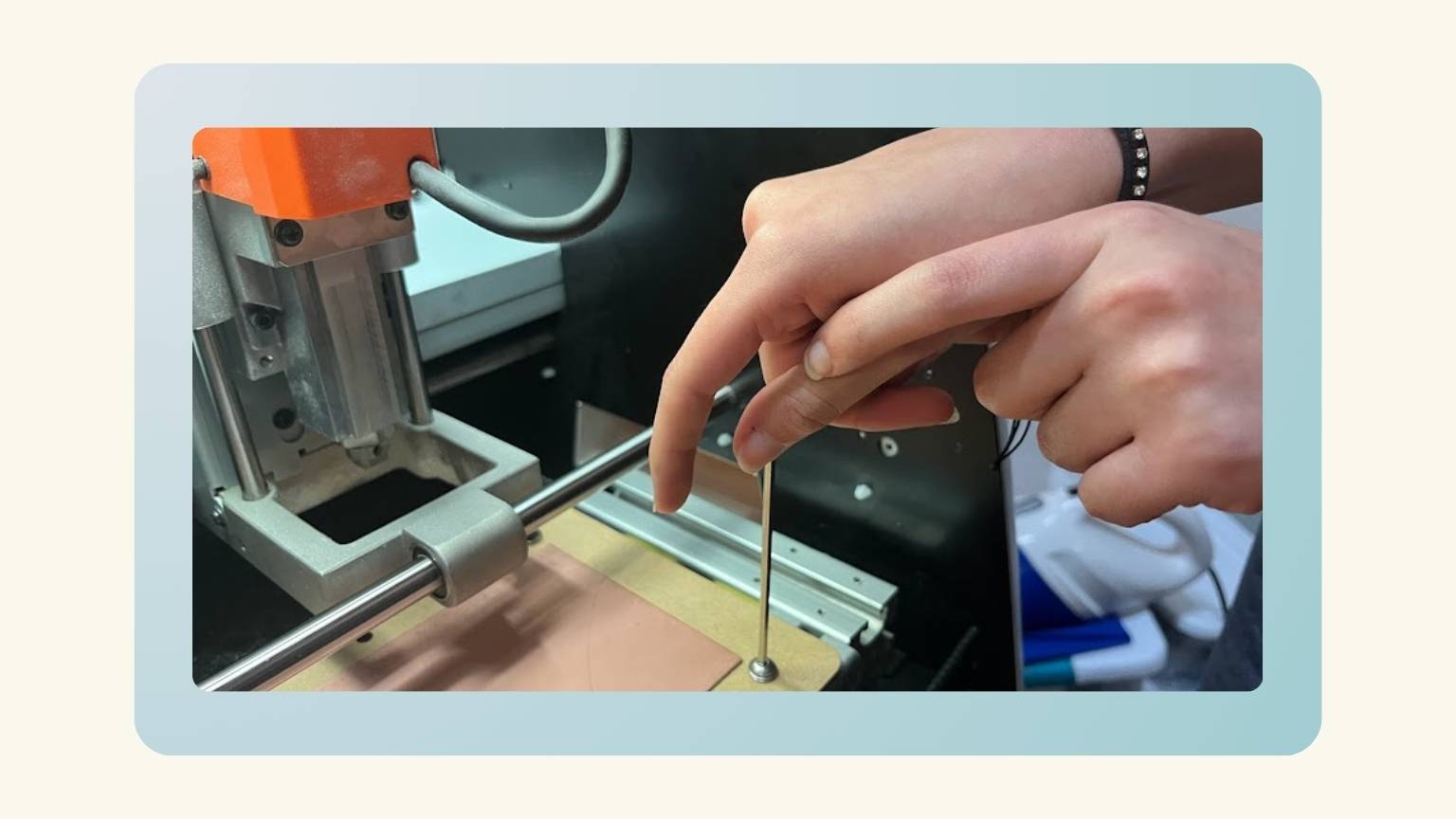
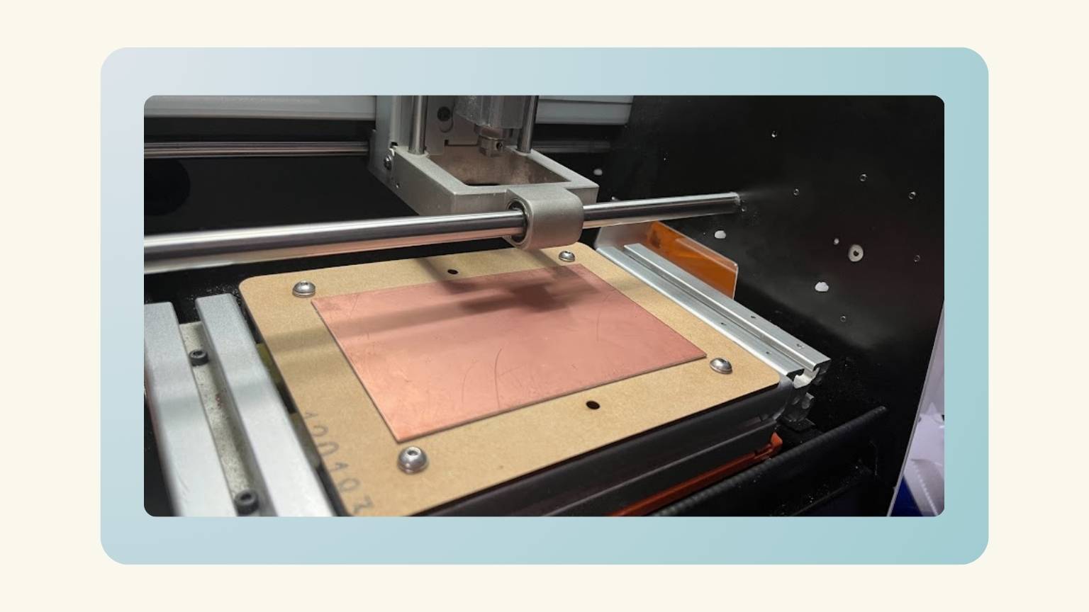
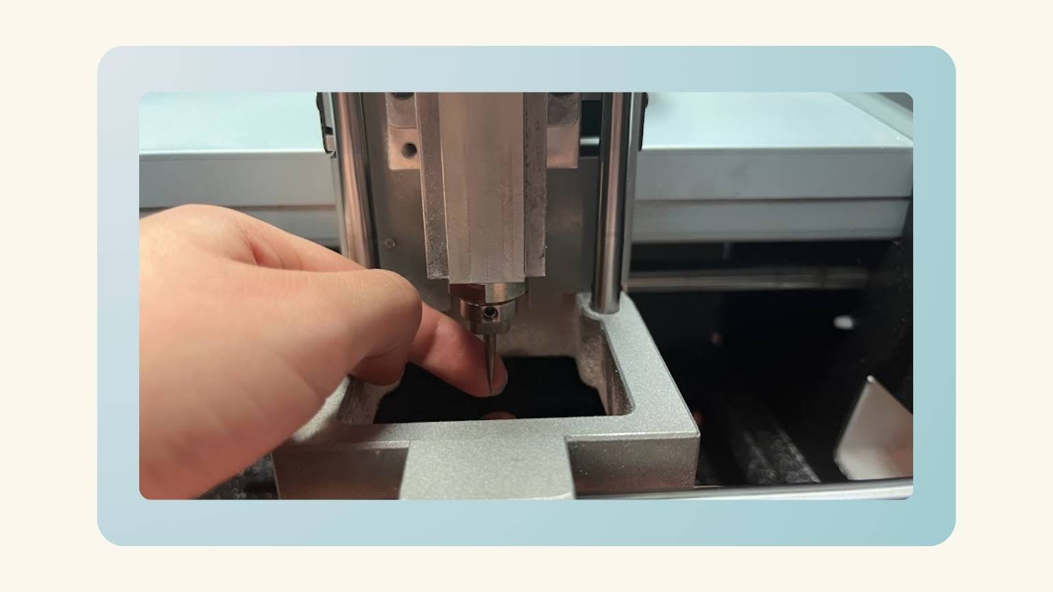
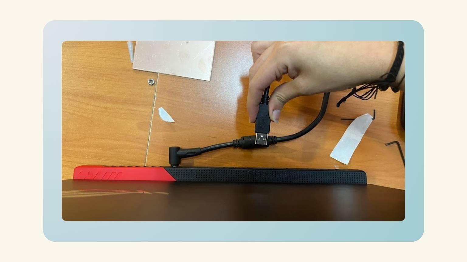
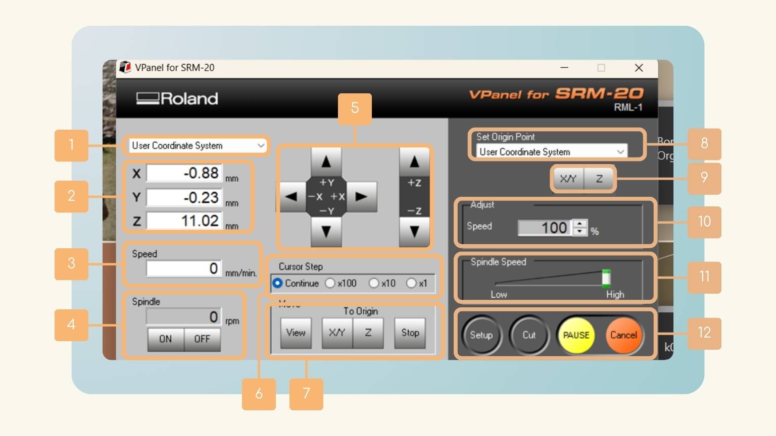
Table of elementes:
| Number | Name | Description |
|---|---|---|
| 1 | Coordinate system | Selects the coordinate system for the coordinate values to display. |
| 2 | Coordinates | The current position of a cutting tool is displayed. he change of mm<=>inch can be performed. |
| 3 | Speed | The movement speed of a cutting tool is displayed./td> |
| 4 | Spindle | In [ON] and [OFF], rotation of a spindle is started and it stops. |
| 5 | Fed buttos | Clicking these buttons moves the spindle head or table. Holding down the buttons performs continuous movement. |
| 6 | Cursor Step | Specify how much the cutting tool should move every time you single-click the [X]/[Y]/[Z] button. |
| 7 | Move |
|
| 8 | Set Origin Point | Select the coordinate system for setting the origin point. |
| 9 | X /Y / Z | Sets the current XY and Z position to the base point. |
| 10 | Adjust | The feeding speed of a cutting tool is adjusted. |
| 11 | Spindle Speed | Adjusts the spindle speed. |
| 12 | Ser up / Cut / Pause / Cancel |
|
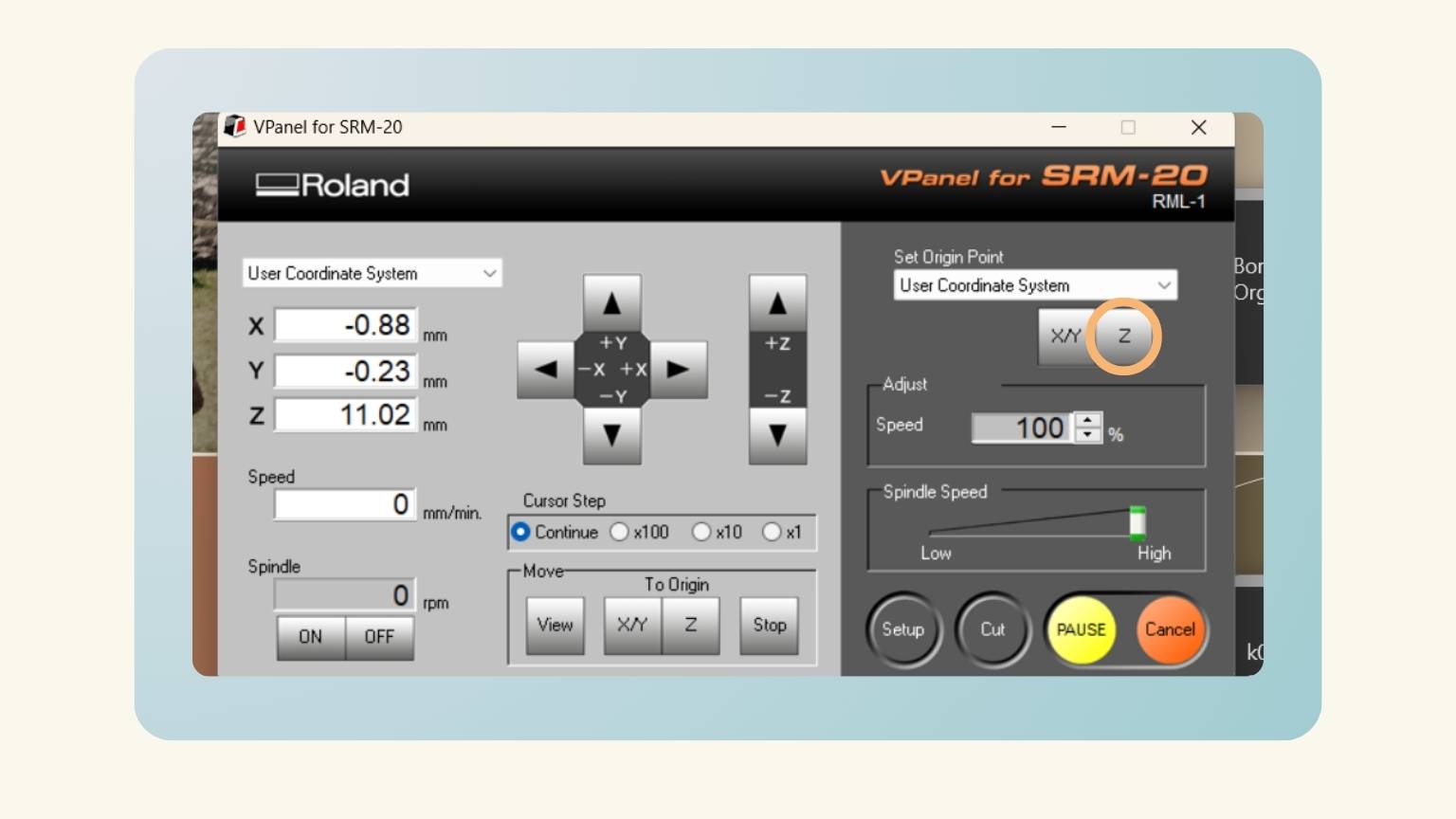
Note:To move the axis fist, I used the ‘Continue’ cursor step, after the ‘x100’ (1 mm), then the ‘x10’ (0.1mm), and finally the ‘x1’ (0.01mm) until the paper generated friction and didn’t come off.

Soldering
What is soldering?
Soldering is the technique of connecting metal pieces to create a mechanical or electrical bond. Soldering involves melting a low-melting-point metal alloy and applying it to metal pieces to glue them together.
- When the solder hardens, it joins the pieces and makes a link.
- Soldering is a common practice for assembling electrical components and wiring.
But... on a printed circuit board?
Soldering is a very typical method for connecting wires or attached components on a printed circuit board (PCB). Copper wires, component leads, and circuit board tracks are typically coated with a thin layer of tin to prevent oxidation and facilitate better bonding with other solderable components. Before joining bare copper wires, we often 'tin' them with molten solder. This creates a stronger link.
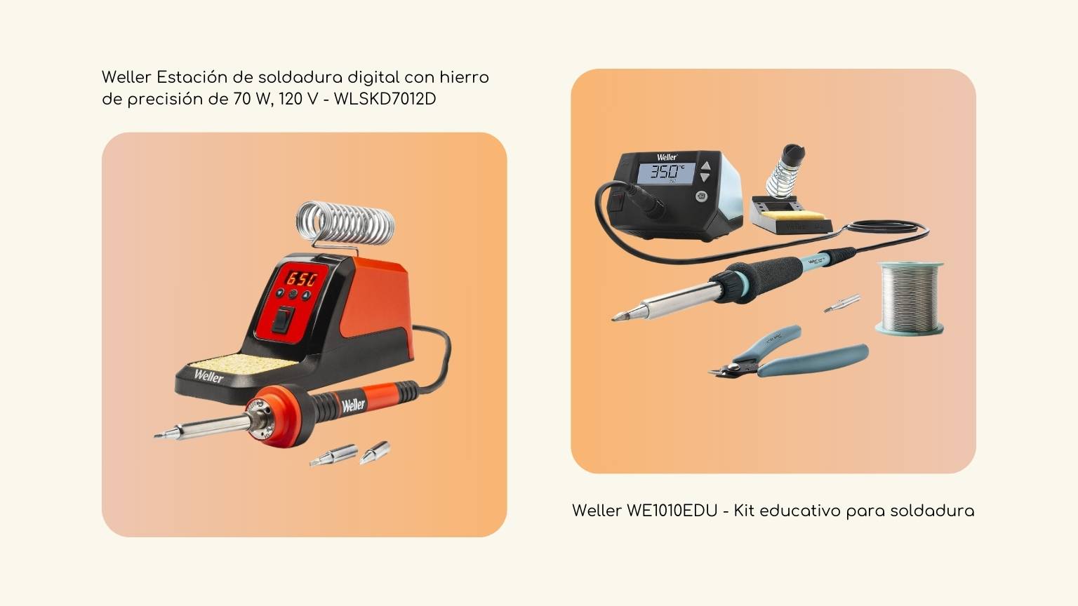
The soldering irons
...You have to be patient when soldering
Practice - Day 1
I had never soldered before… it was a challenge or something like that. So, I had to practice before I messed up my card.
But first, what are the steps for soldering?
- Prepare the PCB or other surface: Start with a clean surface. If your surface isn’t clean, clean it with an industrial cleaning wipe, acetone cleaner, or sand it with fine sandpaper to remove any dust or other debris.
- Apply Some Heat: Time to hold the tip against the lead, make sure not to bend or vibrate the component while you do so, and keep the iron at a steady temperature (around 350°F).
- Inspect the solder joint: If it looks good, move on to the next one.
Note: Before placing my component, I applied a little solder to the place where I would place it, then placed it with the help of tweezers and applied heat with the soldering iron to then apply the tin. I did this to make it easier to place the component to be soldered.
Start soldering!
I started soldering, and it was difficult to understand how to know that my surface was already heated for tin application. That said, I have had it happen to me that I would heat up my board, apply the thin, and see nothing happen.
Another point was that I couldn’t find a comfortable position for soldering… It took me a long time to find it.
- For example, to pick up the soldering iron, I took the same position I took when picking up a pencil, but this wasn’t safe as I particularly tend to grip the pencil from the bottom and hide my big toe.
- The good news is that I managed to take it well!
I think it was a good first approach.
Practice - Day 2
I practice a little more to put only tin on a card. After that, I started practicing soldering components on a test board.
Some people told me that soldering on the test board wasn’t the same as soldering on the copper board, so I started testing on a small board. In doing this, I realized the following points:
- It was different soldering on the copper board.
- I still had the problem of not placing the solder correctly on the board because the solder remained on the tip of the soldering iron.
- This made me use a bad technique, which I later corrected. The mistake was that when I saw that it was stuck on the tip of the soldering iron, I put it back in this way, and when it heated up, I brought the solder closer again so that something would fall on the plate.
- The choice of the soldering iron is important because it has a different tin, and some help you, but others do the opposite.
- Practice helps, but time is running out.
Start with the components
After practice, I decided to venture out and start soldering the components on my board. So as per the recommendations, I decided to start placing the resistors since they were the smallest parts.
I was very happy with the results… but I didn’t know what would happen next.
Practice - Day 3... The Day?
Day three… and I continued practicing a bit before putting the missing components back on my board.
- After analyzing this, I think I was too afraid of ruining my card.
Anyway, I started soldering the missing components, and I realized the following:
- The process is faster than I thought with practice... or not?
- Bending the pins was complicated.
- And the same by soldering them. I had to ask my sister to help hold them with the clamp as I heated the board and put the tin on.
Note: When soldering, I started with the resistors, continued with the button, from there with the pins, and finally with the xiao.
Programming… does it work or not?
To program the PCB, I followed the next steps:
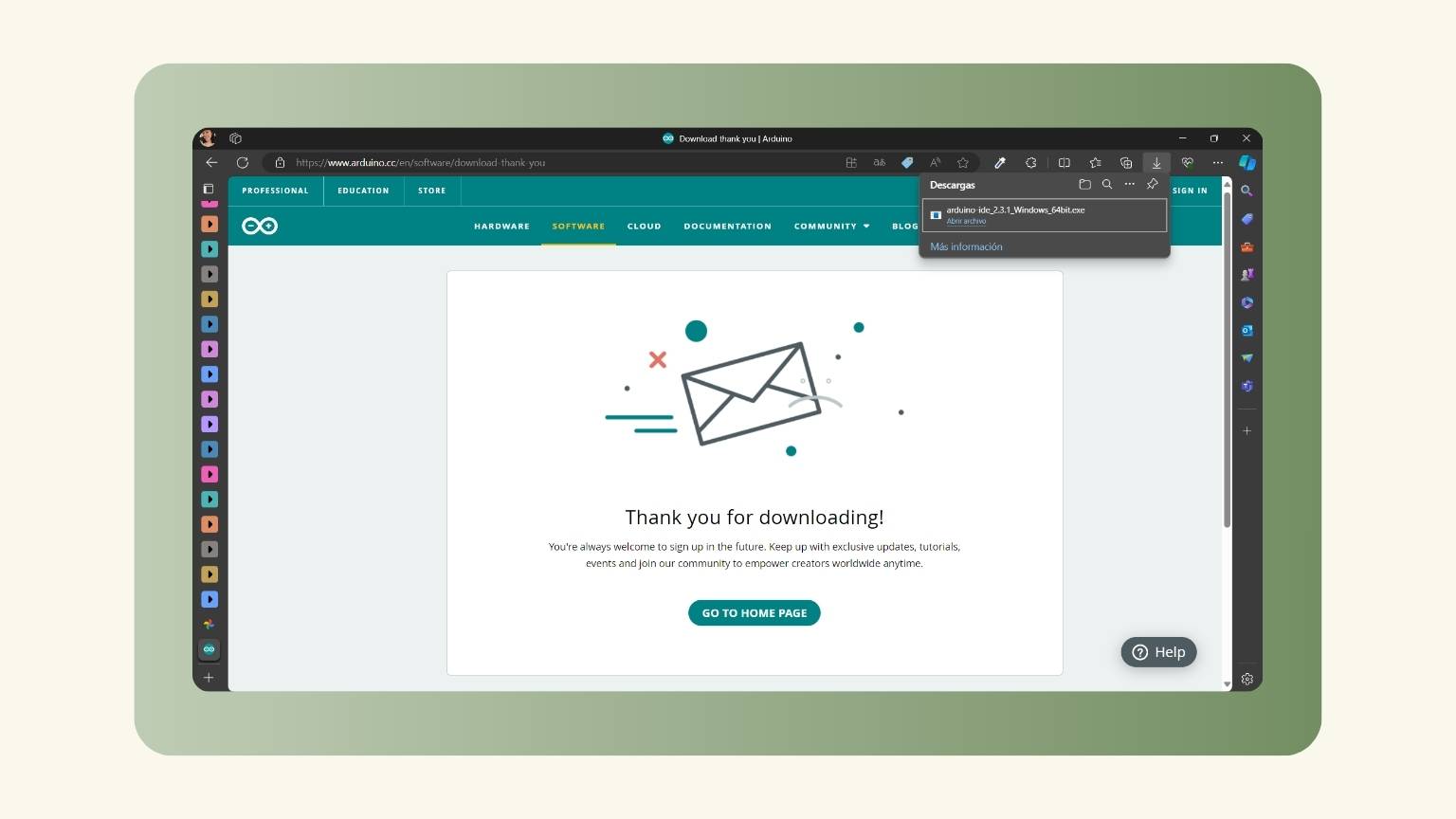
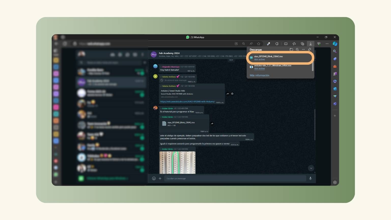
- I downloaded Arduino.
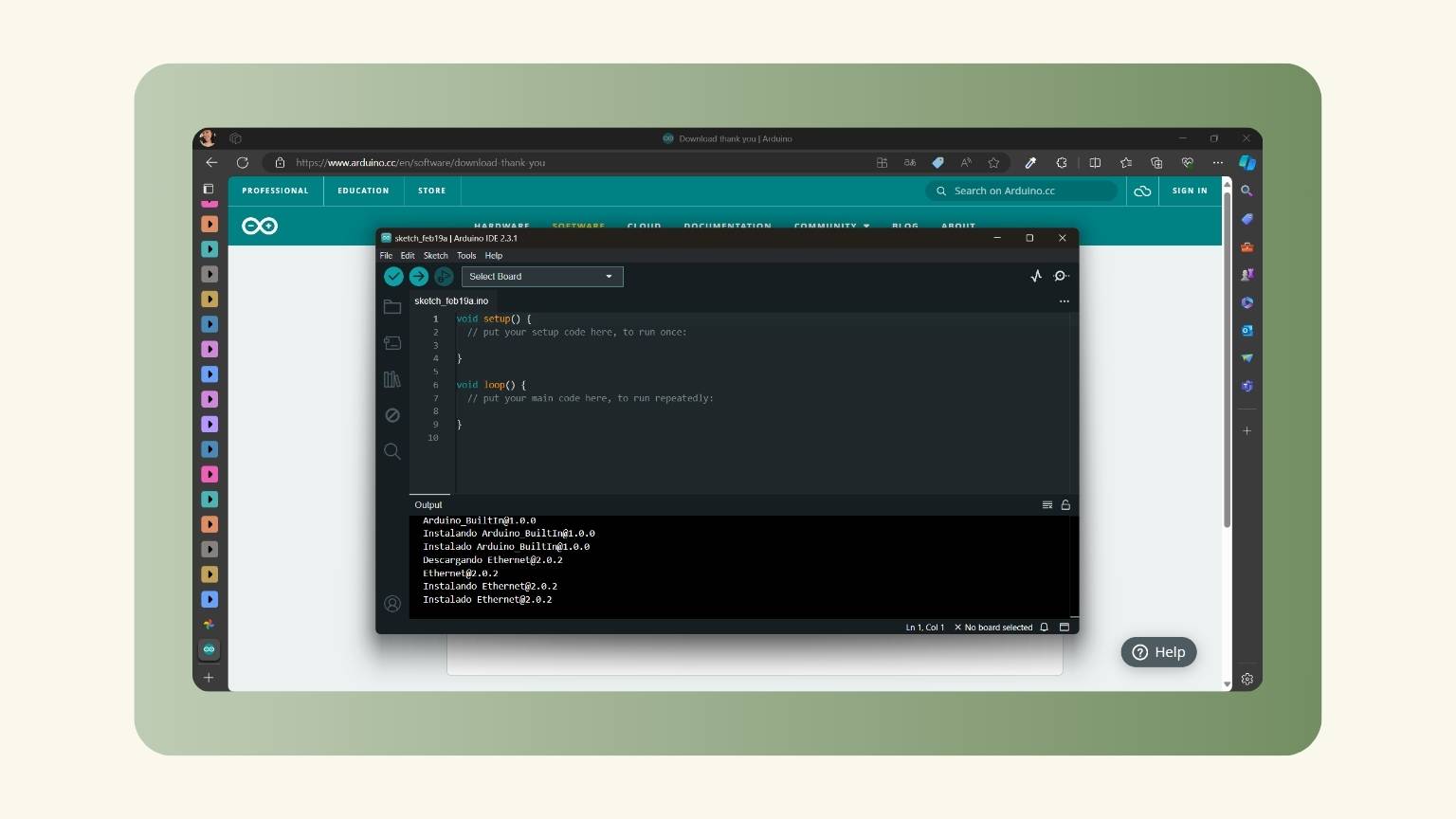
- When the installation was ending, I opened the software.
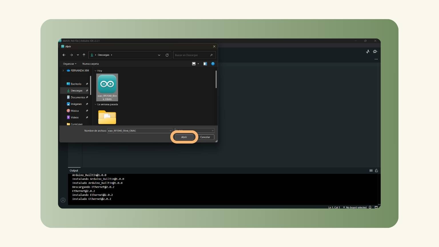
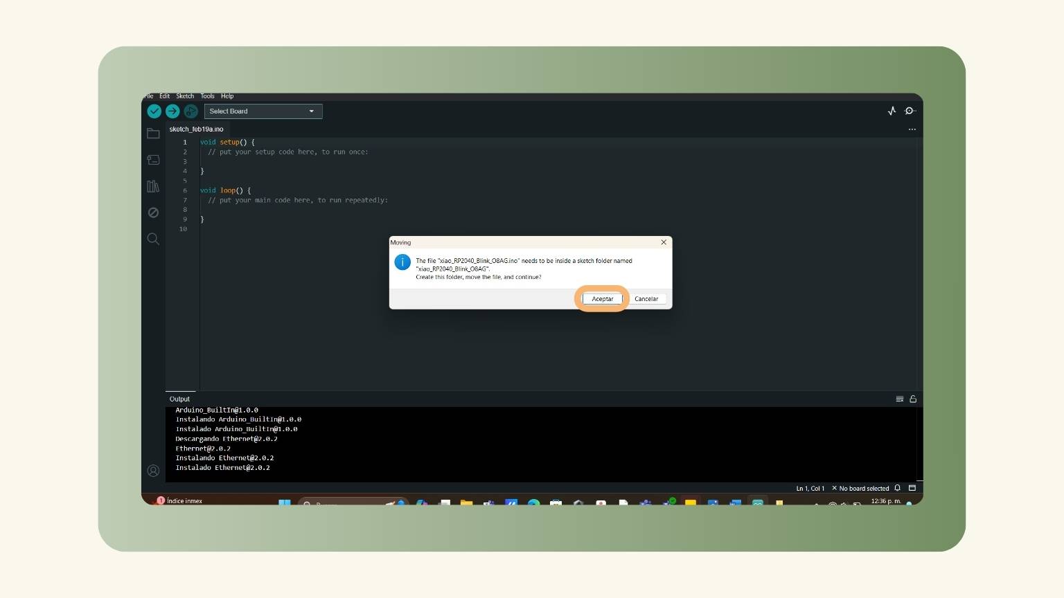
- I downloaded the code example that brought us.
- I opened the file in Arduino.
- I was prompted to create another folder to open the file in, and I said yes.
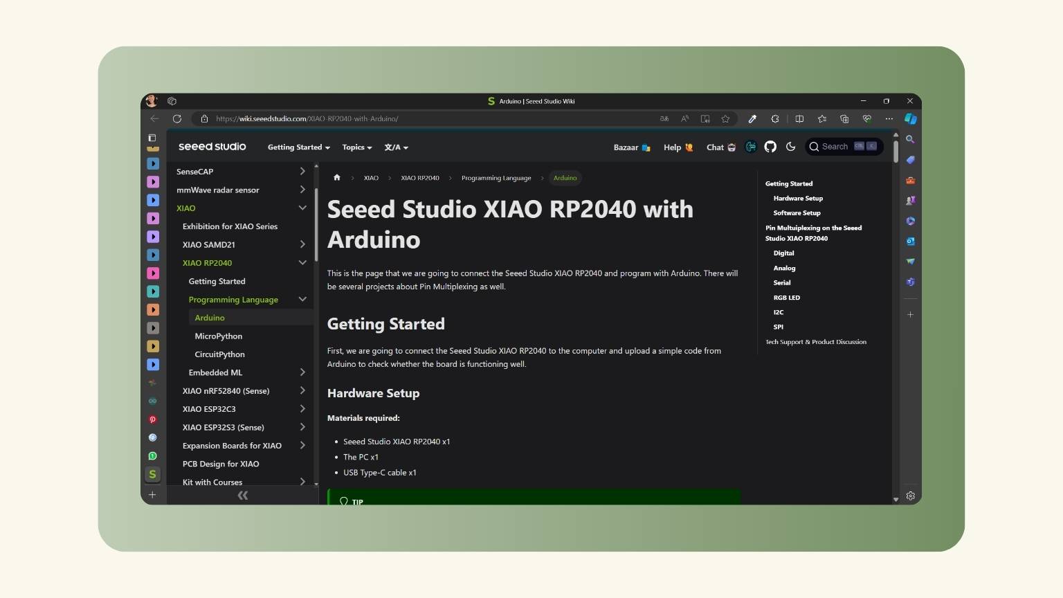
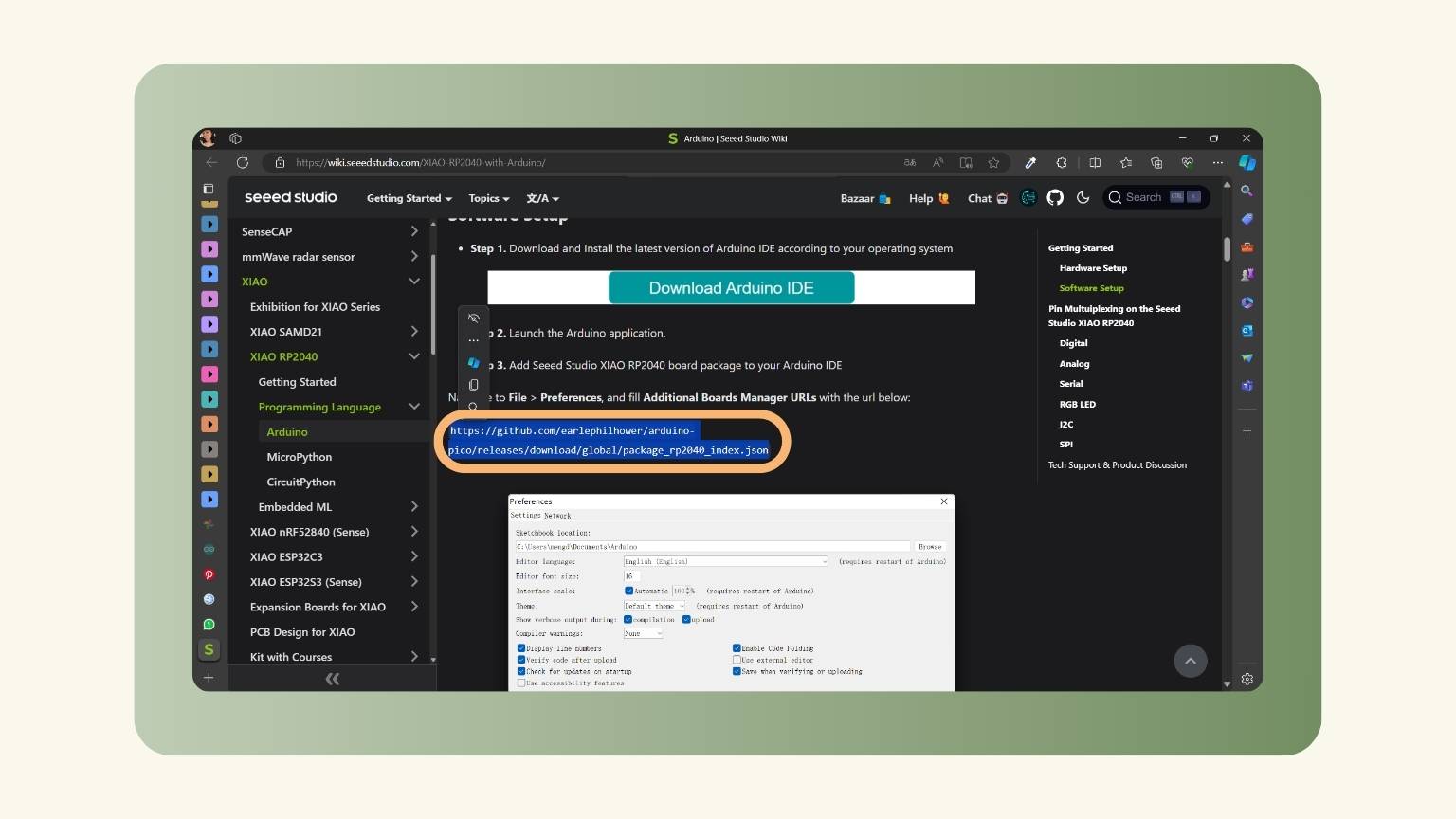
- I went to the website of the Xiao that we used.
- And I found the URL that it should be placed in the preferences of Arduino.
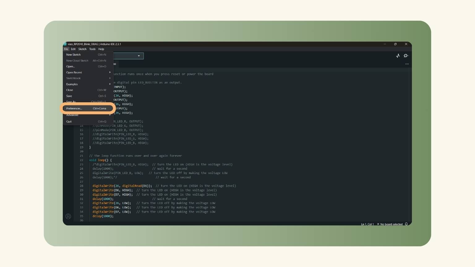
- I clicked on ‘File’ and found ‘Preferences’.
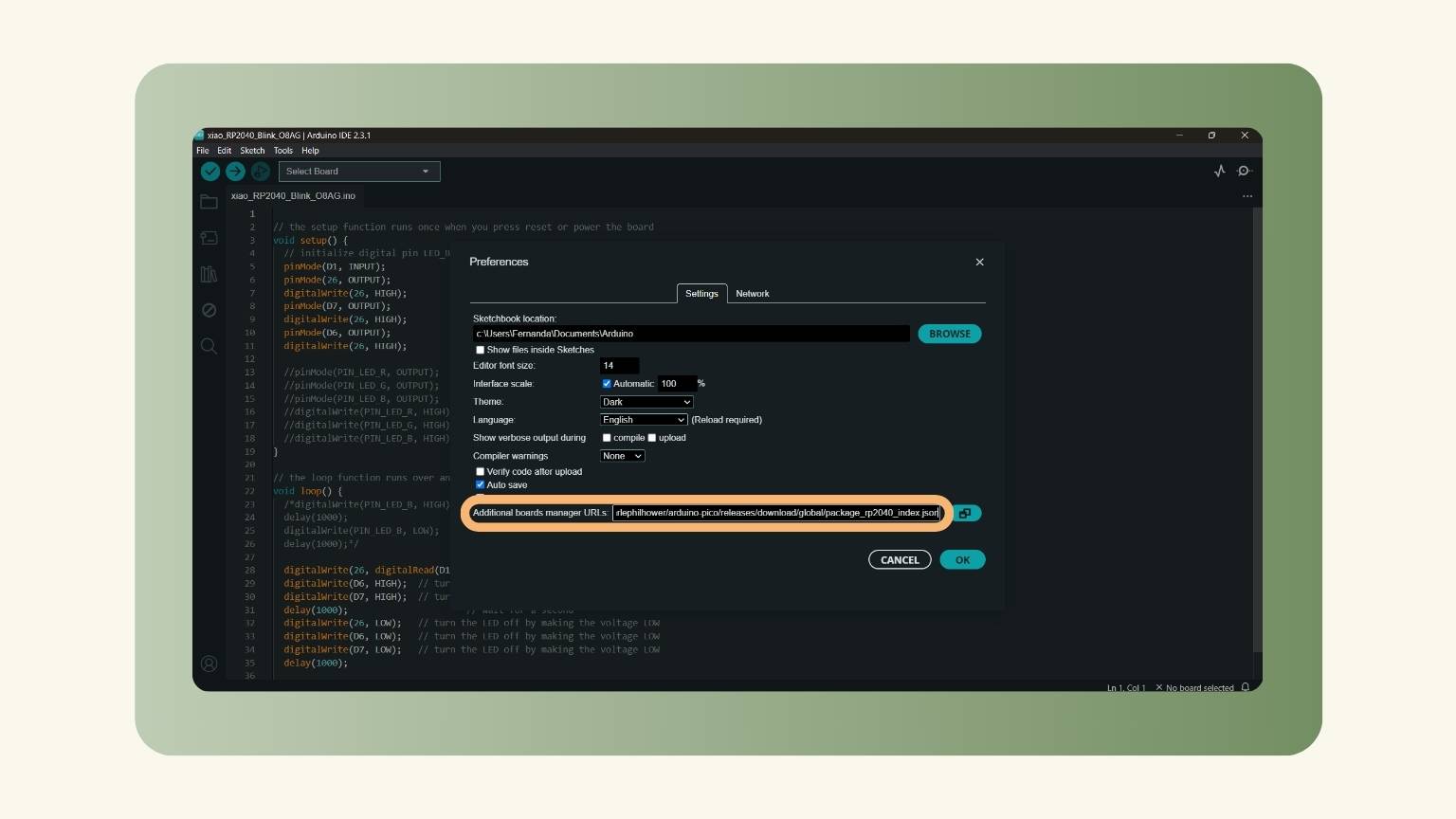
- In ‘Preferences’, I pasted the URL that I copied in the section of ‘Additional boards manager URLs’. And I pressed ‘OK’.
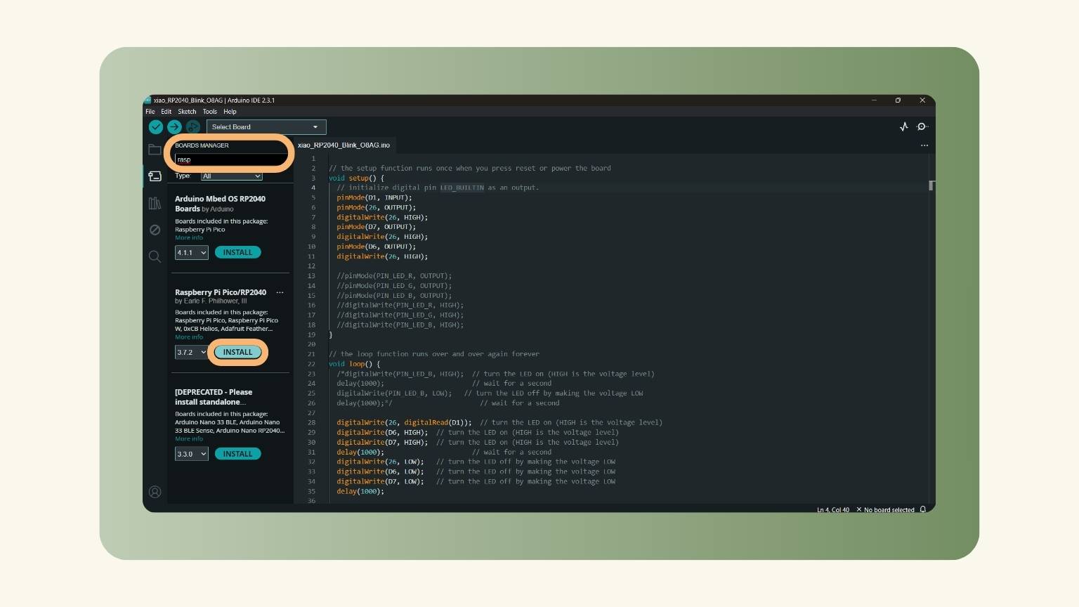
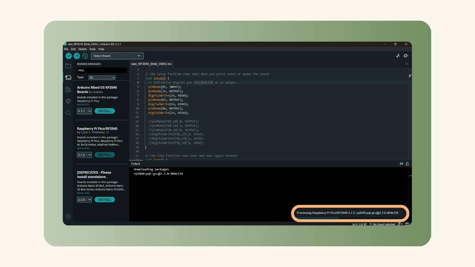
- Then, in the ‘Boards Manager’ I searched for raspberry and installed the second option,
‘Raspberry Pi Pico/RP2040’
- Pay attention to installing the option that says ‘3.7.2’.
- The installation was processed.
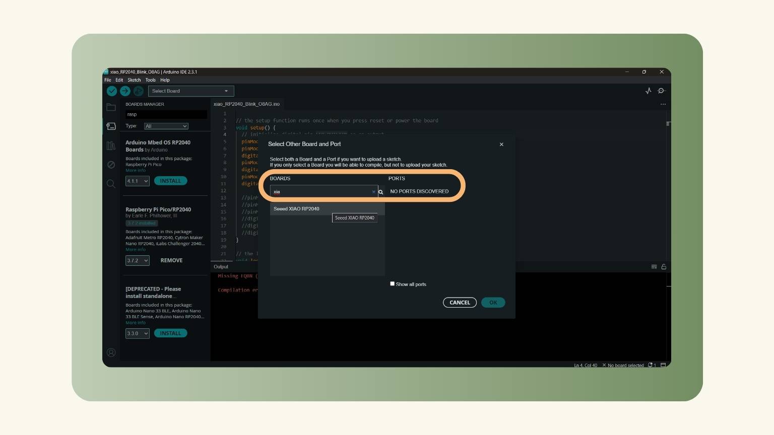
- I pressed the menu of ‘Select Board’ to put the board of the xiao, the option ‘SeedXIAO RP2040’.
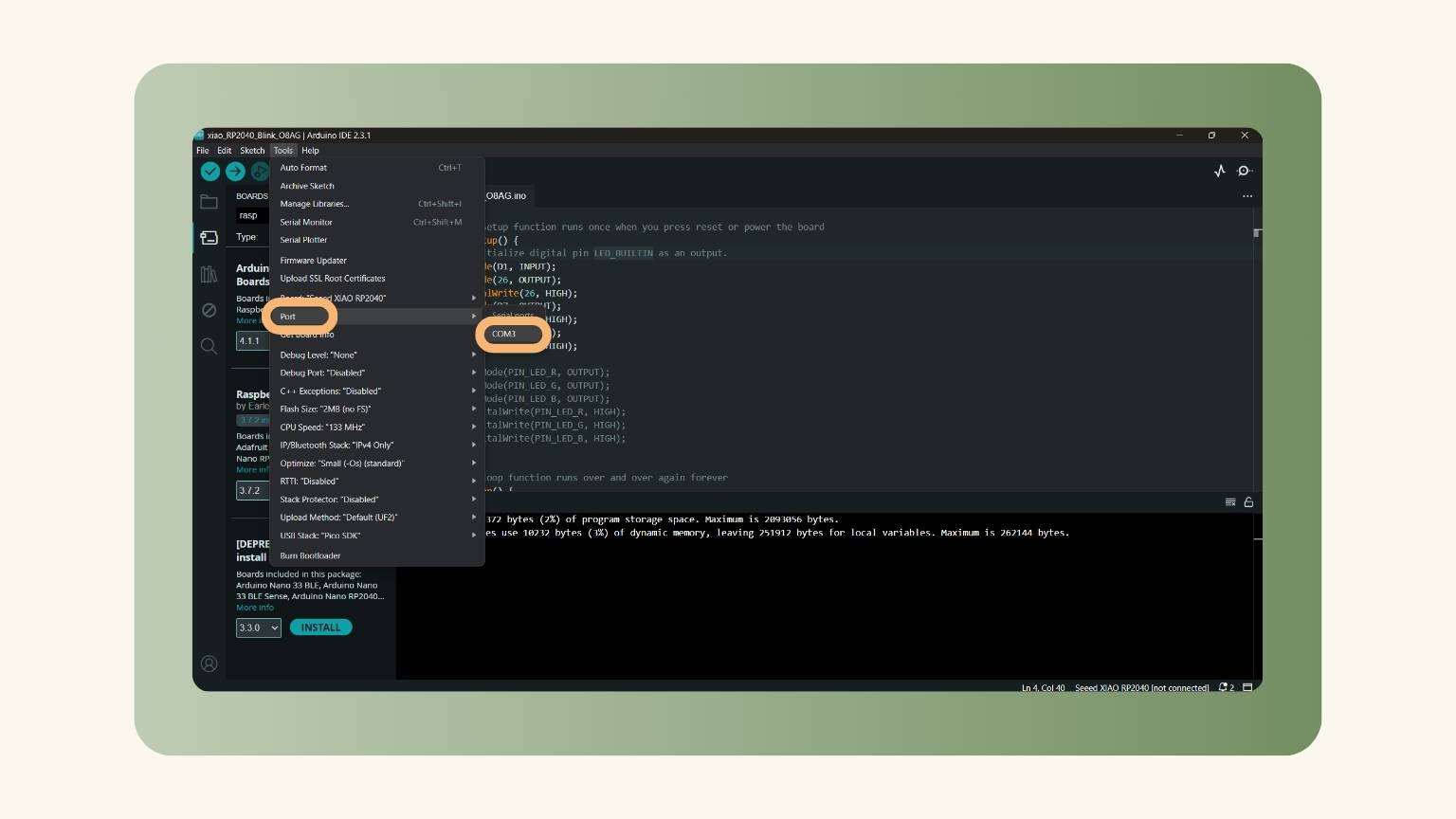
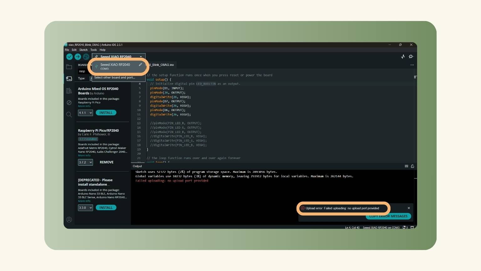
- I have problems with my port, but I resolved them. And I went to the menu of ‘Tools’ and found the ‘Port’ option to select my port.
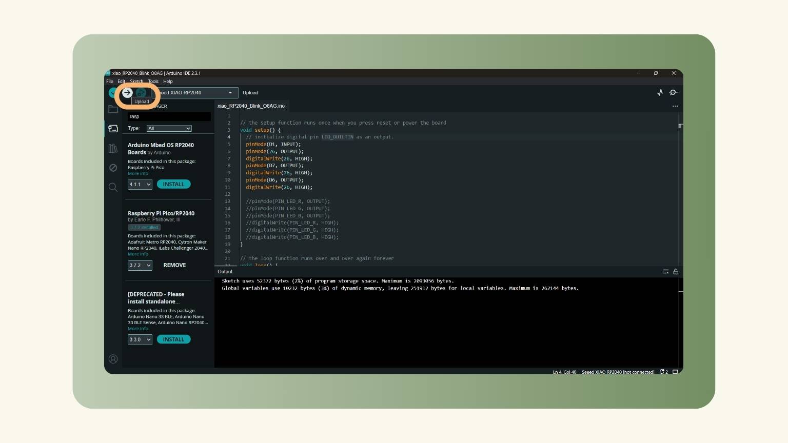
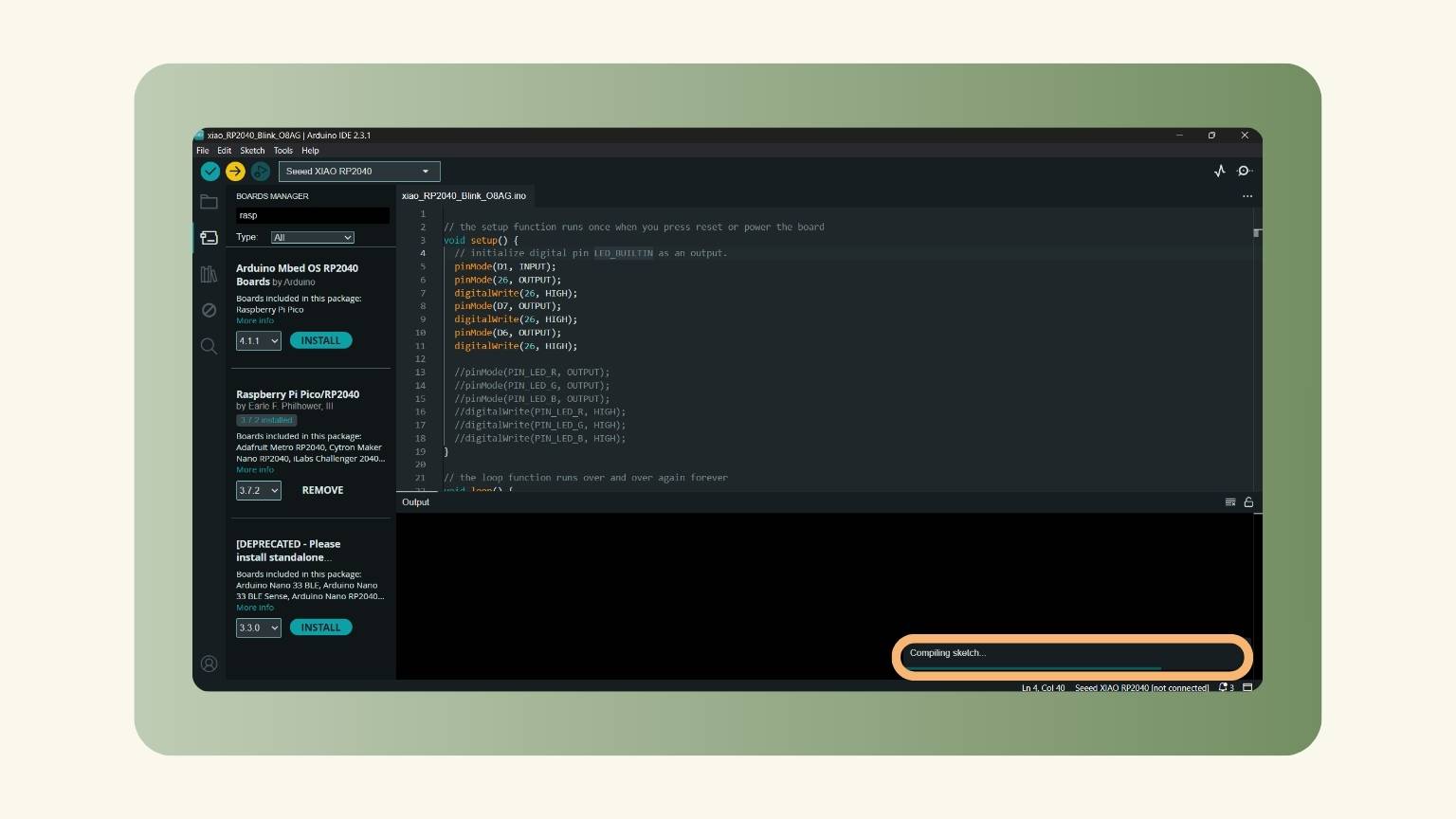
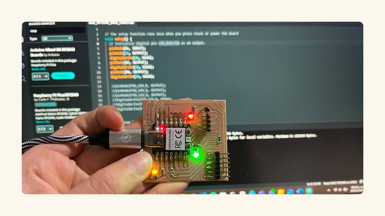
- I uploaded the code.
- It was compiled.
- There was an error in the upload. So I returned to the ‘Select Board’ and selected ‘ SeedXIAO RP2040 COM3’, the option with the board and port.
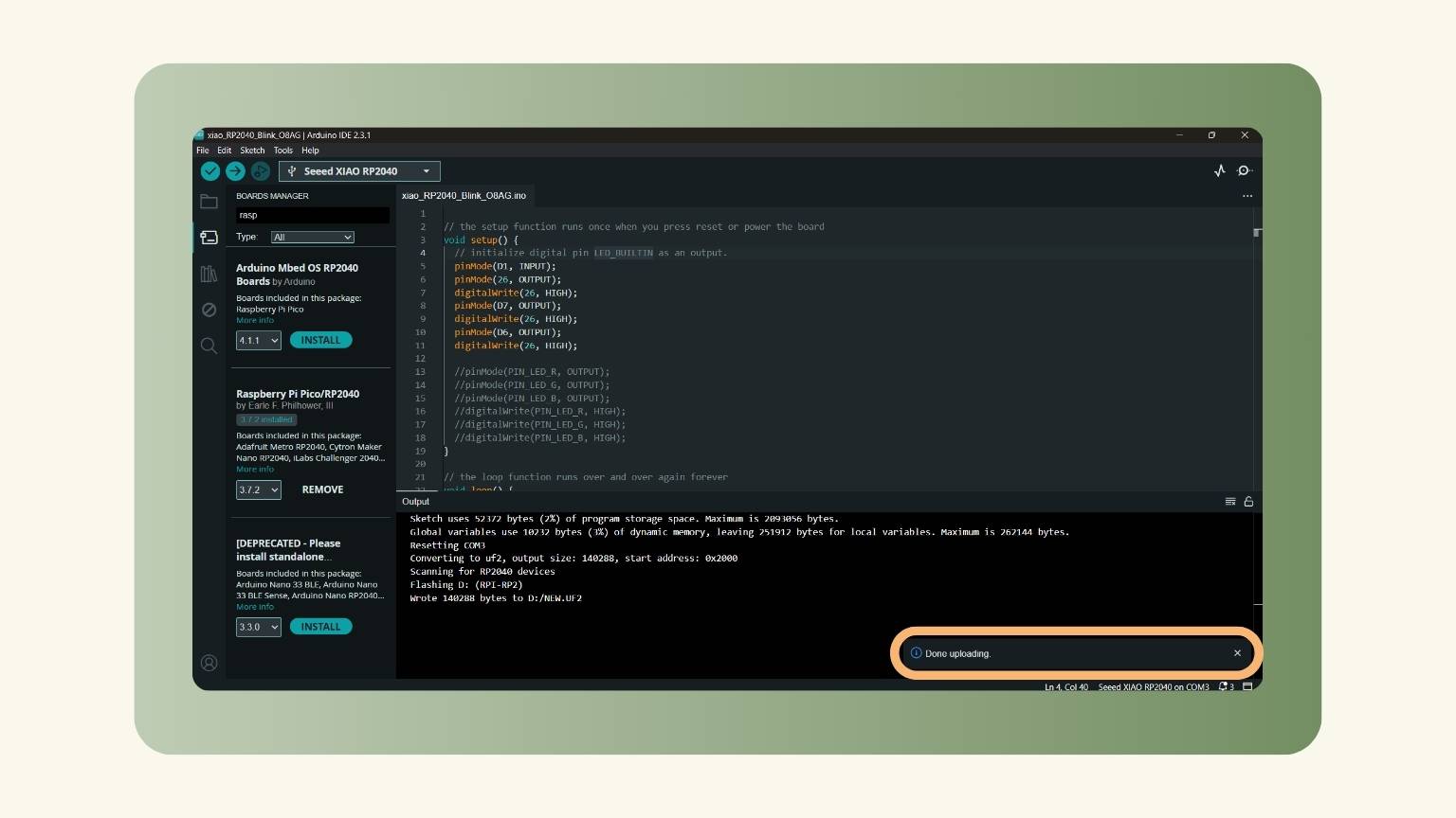
- The code was compiled.
- The upload was done.

Arduino Code
Desoldering… and the chaos
When I connected it and loaded the code for the first time, it failed… and the desperation started.
The first thing I thought was the error was a higher KΩ resistor that I used because a colleague had the same failure, and when I changed the component, the problem was solved. So, I changed the component, and I proved it, but it still had the fault.
- I desoldering the resistor and placed one like the ones already had.
I came to the second theory of the failure: that soldering was needed on the xiao and on the LED that did not light up. So, I applied more solder to these areas and retested, although the fault persisted.
- I soldered a little more on the xiao and led.
We then continued with the search for the fault and came up with two thoughts: (1) that one of my leads on the board was destroyed and the solder didn't have joined, or (2) that one solder had joined with another and that created a connection that should not be there.
So before considering point one, I unsoldered the resistor that was theoretically causing the conflict to remove the tin that could be covering up the error and found that everything was fine, so I went back to soldering to test... and it still didn't work.
Curiously later, we discovered that the mistake from the beginning was that when I re-soldered the resistor, I had burned it... Therefore, I unsoldered it again to put in a new one, and it finally worked.
The final result
… it’s woks!
Conclusion
During this week, I have learned several things since it is a subject that I did not know and from which I was very far away. However, I think that despite the speed of the week, I have been able to learn and get to know the subject in a broad way.
Some things that I must reinforce from this learning are: understanding how the multimeter works; practicing my soldering more; understanding how resistor equivalencies work; and understanding the function of each component.
And I'm not sure that soldering is like dancing... But in the case of the one that does, I’m not sure which one I would prefer… Both have their difficulties.