
4. Electronics Production
This week, I was able to fabricate and assemble a previously designed electronics board, which incorporates a XIAO RP2040 module, a button, three LED's and some pin headers!
Preparing The Design:
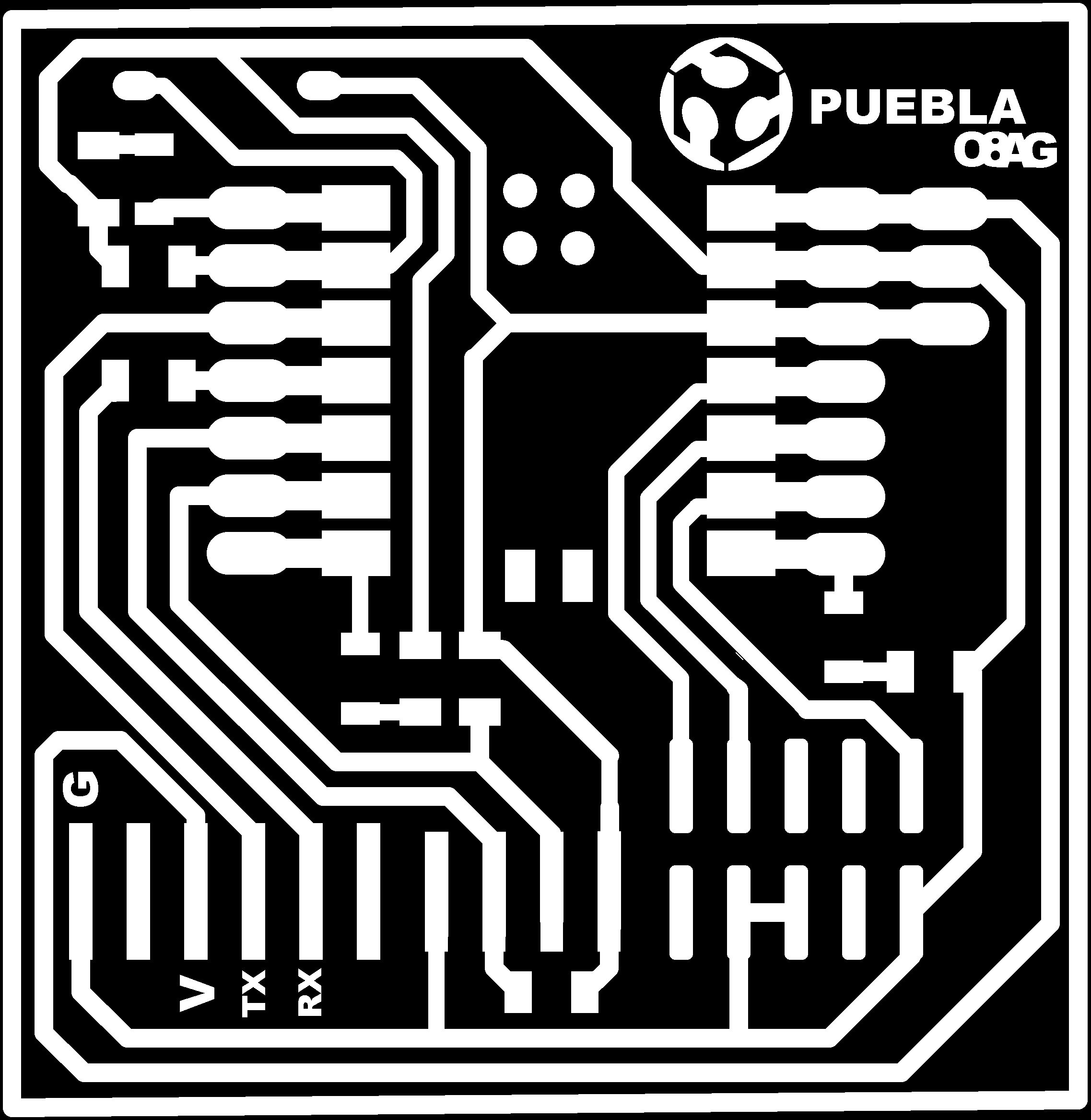
The design for the board, at least to be engraved on a the phenolic board using a mini-Mill machine, consists of two black and white images, which contains both the milling pattern and board dimensions. Although the data is somewhat on there, we need to extrapolate it and turn the images into G-Code: A way the milling machine can understand the instructions to create the image on the board.
As I said, we have this two .png images that show the engraving pattern (left) and cutting pattern (right):

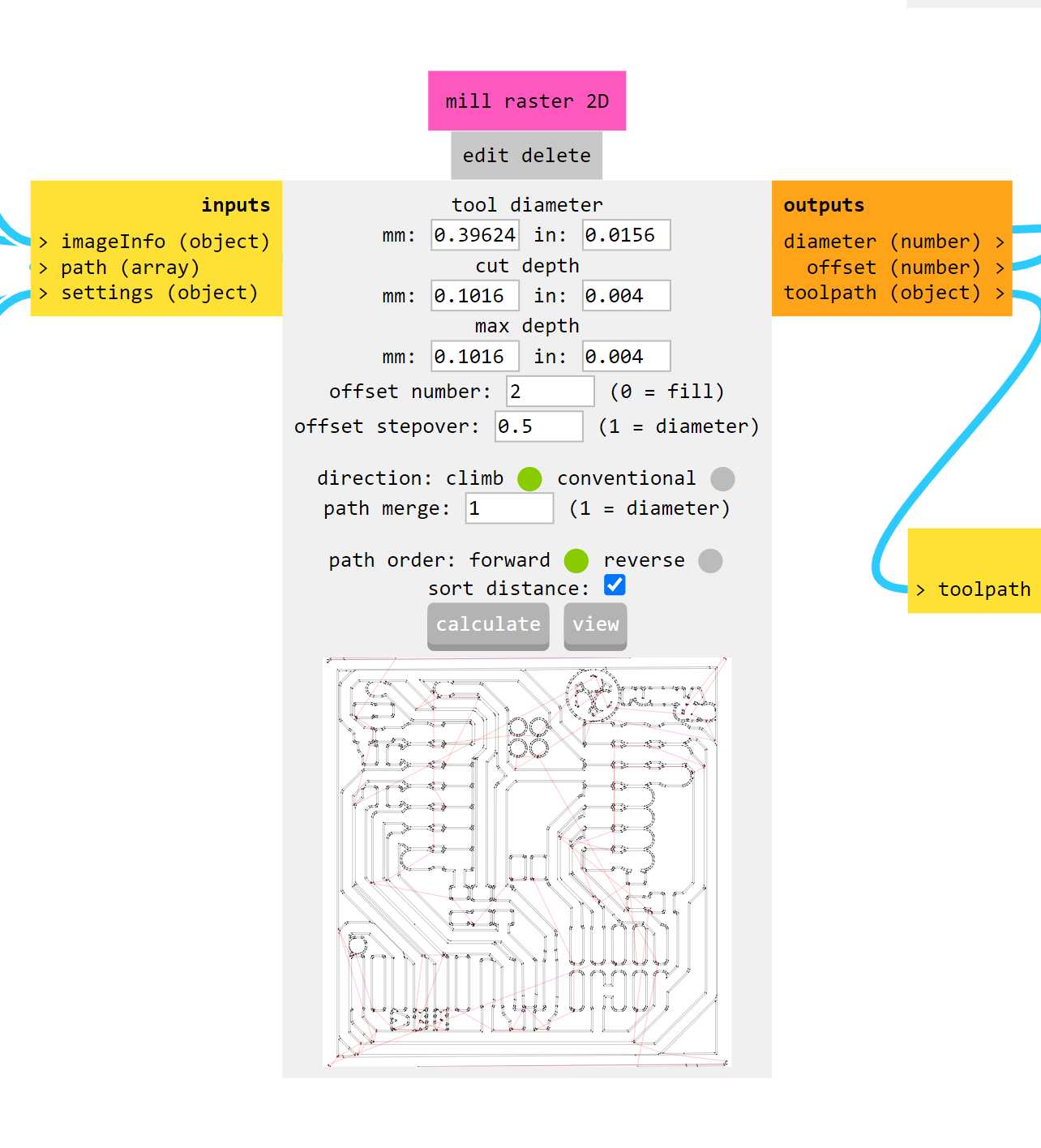
Then, we have to create the G-Code from those images so we can upload it to the milling machine. To do this we use the .png to G-Code converter listed on the modsproject webpage! Once we are on the site, we right-click and select programs -> open program and then we look for the model of our machine, in my case an SRM-20 from Roland. Under the list for the SRM-20 we select "mill 2D PCB". Following those steps a huge node diagram will open:
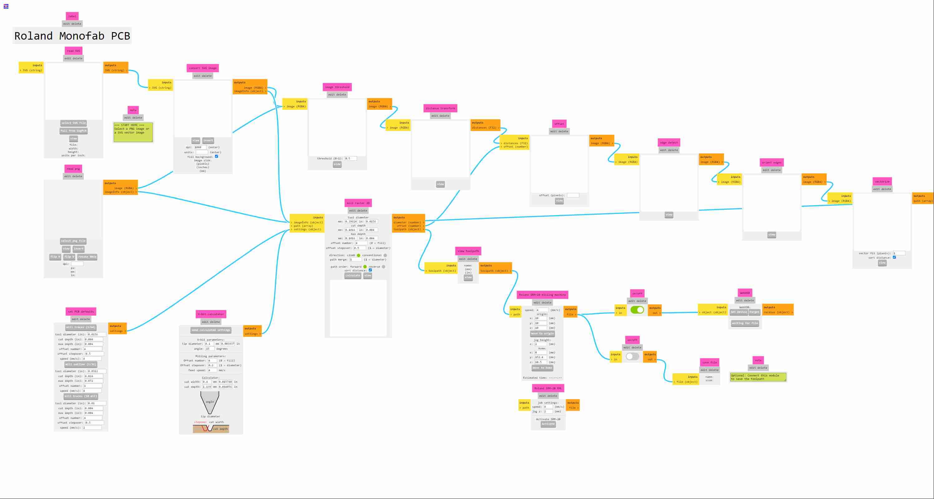
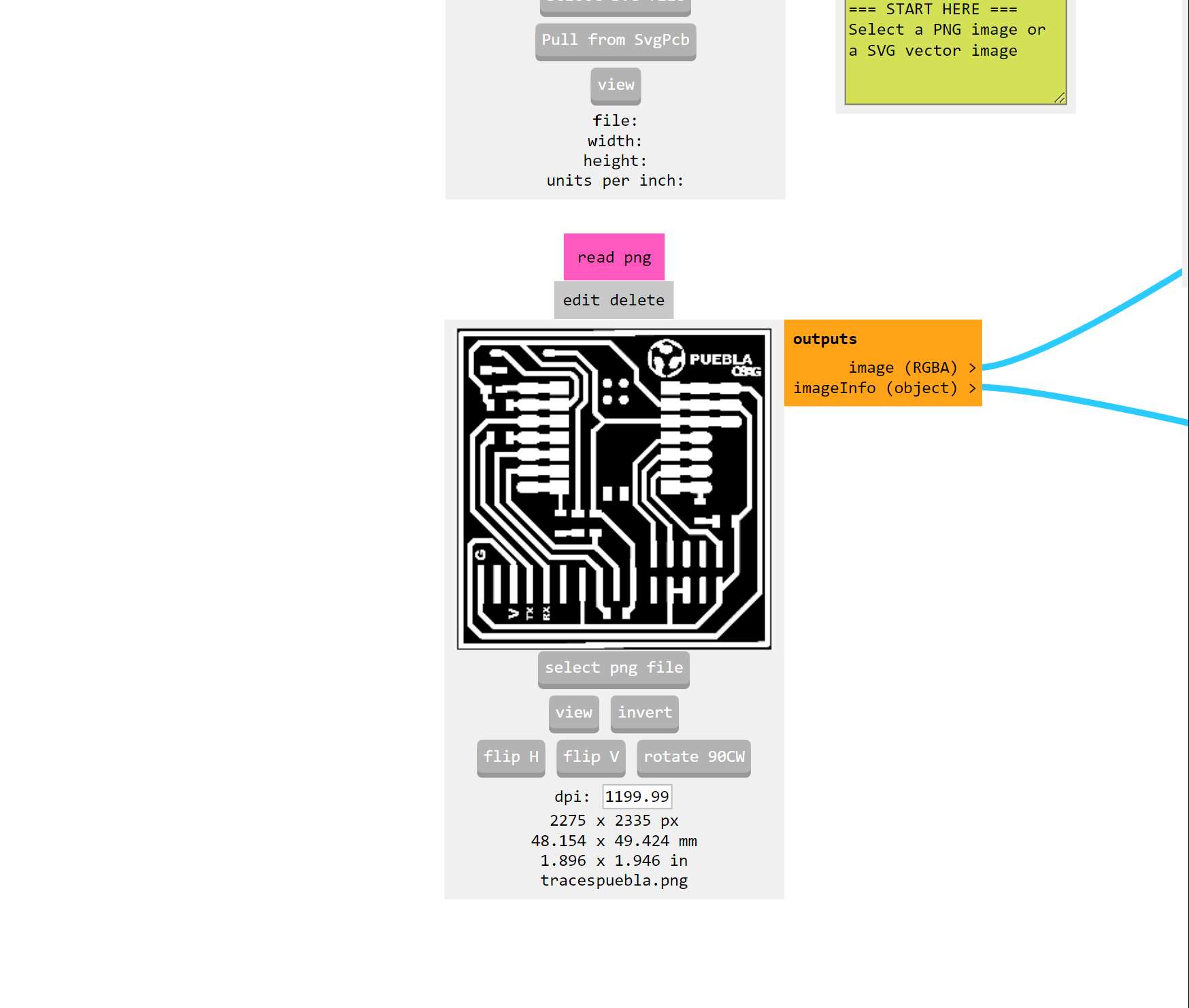
This window may seem overwhelming, but we don't have to modify much on it, so it turns out to be very easy. To start our conversion process, we look for this module on the diagram and upload the .png image using the "select png file" button:
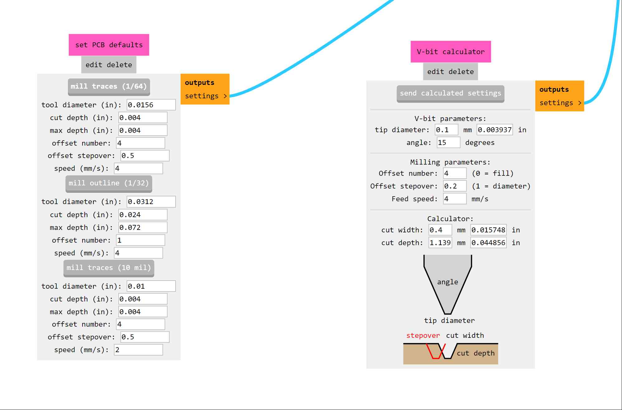
Once this is done, let's go and change the cutting parameters to the ones shown on the image, after testing I saw that an offset of 4 (The amount of overpasses the milling tool does over a cutting path) works well with the 1 oz FR-4 phenolic boards we had available. Also, we have to input the correct properties for the milling tool we are going to use.
After this, we have to set the origin coordinates, relative to the image, on the point (0,0). Also, we have to activate the switch inside of the drawn blue circle, this is to indicate the program to export the G-Code as a downloadable file:
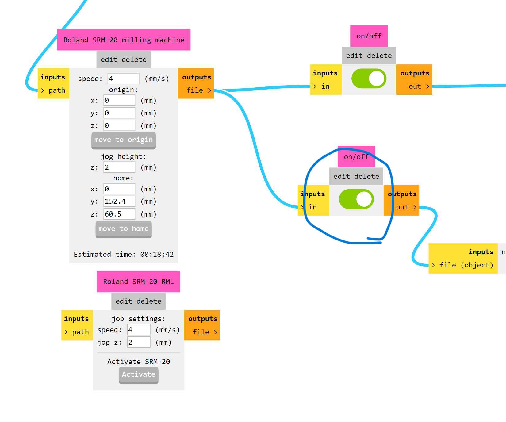
When finished doing all the steps mentioned before, we can head onto the calculation module, when clicking "Calculate" a new window on our browser will open, and a file download will automatically start. That file is the G-Code for the PCB traces pattern!
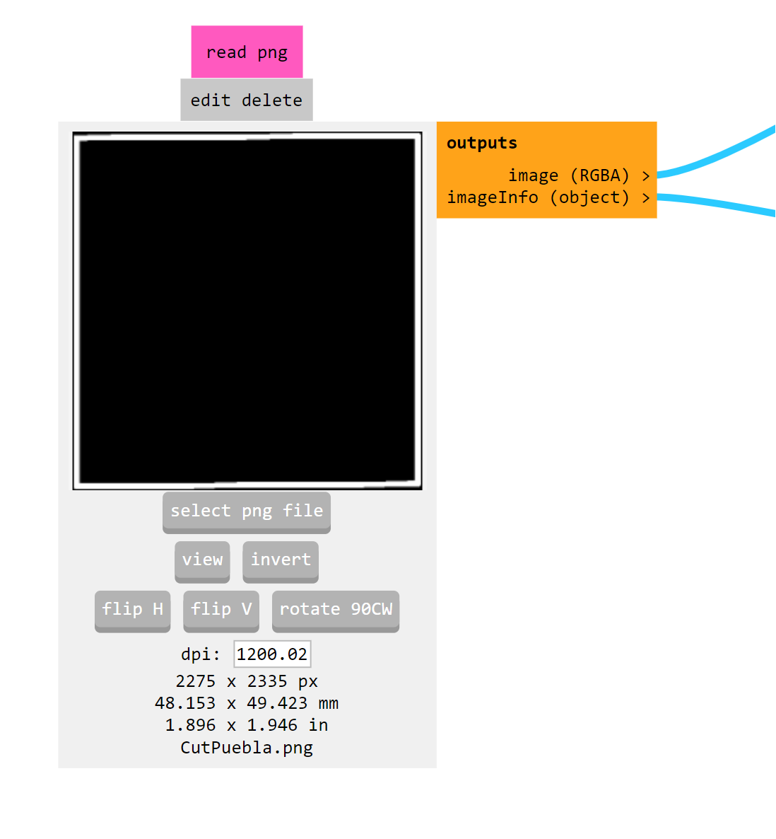
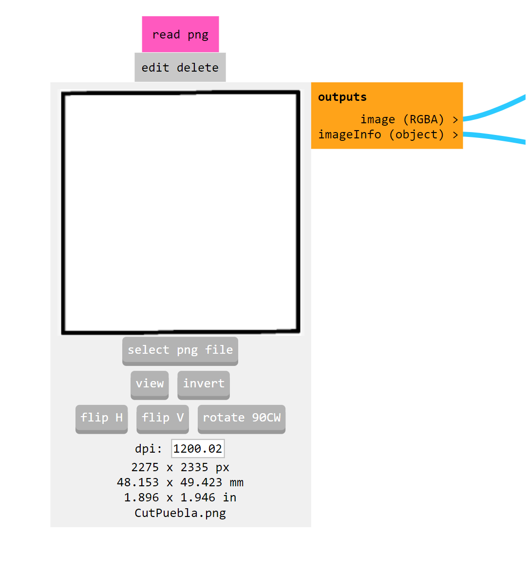
That G-Code is for the traces only, so we have to import the outline cutting pattern image onto the same process, the only difference: We have to invert the image when imported using the "invert" button, this is because the program interprets black as the cutting area. We can see the effects of inverting the image below. Original (left) and Inverted (right):
Preparing the Phenolic Board:
Before doing the actual cutting of the board, we first have to prepare it by mounting it on a laser-cutted 3mm MDF board called the "Sacrifice Board". This board serves as a protective layer between the milling machine's metallic bed and the actual phenolic board, as it is common during cutting, that the tool goes deeper than the thickness of the material, resulting in tool or bed damage. The soft MDF layer allows for the tool to cut over it without damage. It has holes meant for it to be mounted onto the machine's bed with ease.
Once the phenolic board is mounted on the MDF board using double-sided tape, we can proceed with the cutting.
Milling the PCB Patterns:
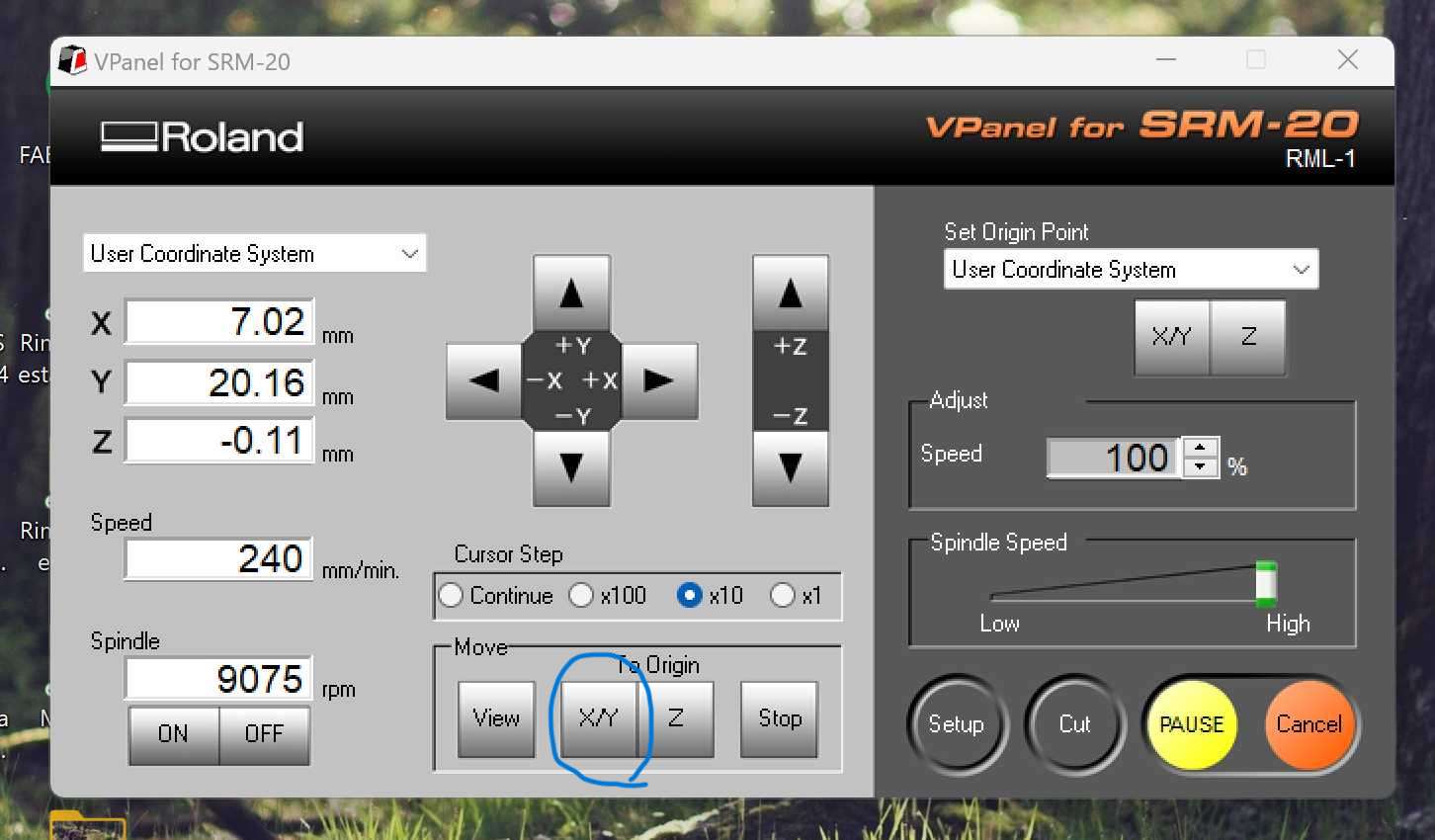
Using the "Vpanel" software provided by the milling machine's manufacturer we can manually move the cutting head along its 3-axis, using that interface we try to set the machine's origin to a point where our circuit fits onto the phenolic board and doesn't waste too much space. In may case, I placed it on the bottom left corner. Once we're satisfied with the origin's position we set it by clicking on the "X/Y" button below the "Set Origin Point" legend, as indicated by the blue circle.
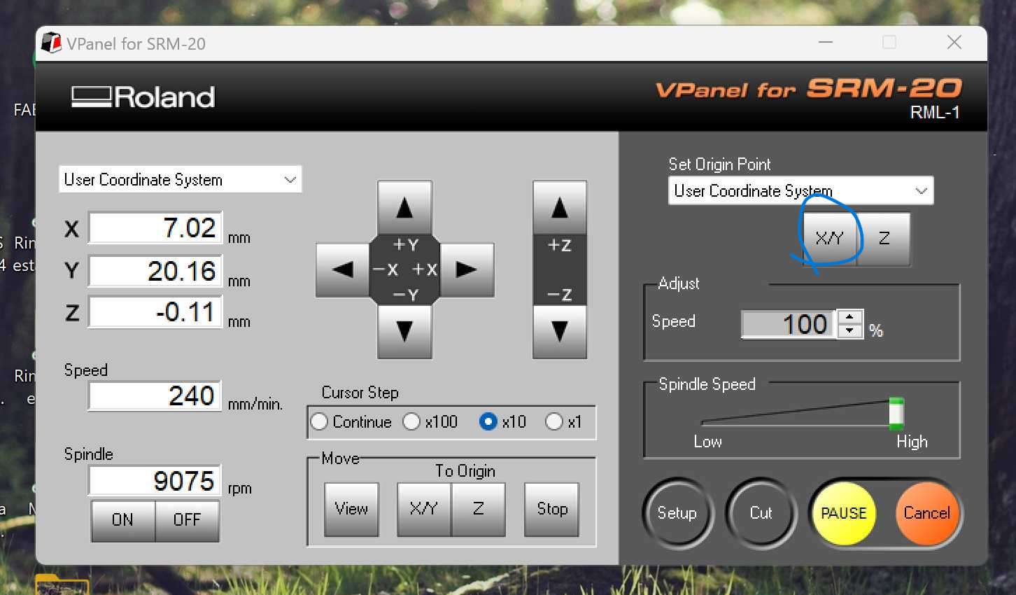
Once the X/Y origin is set, we can adjust the cutting head's height: lowering the Z axis milimeter by milimeter and placing a piece of paper below it until it gets slightly "trapped" between the tool and the board is a good way to know how low the tool should be. Once we're satisfied with the tool's height, we set the Z axis origin clicking on the "Z" button below the "Set Origin Point" legend.
We can now upload the PCB pattern's G-Code file onto the Vpanel software. Click on the "Setup" button and select your respective file. If everything seems right, you can click the "Start" button to machine your board. The process should start inmediately after the tool's spindle gets up to speed.
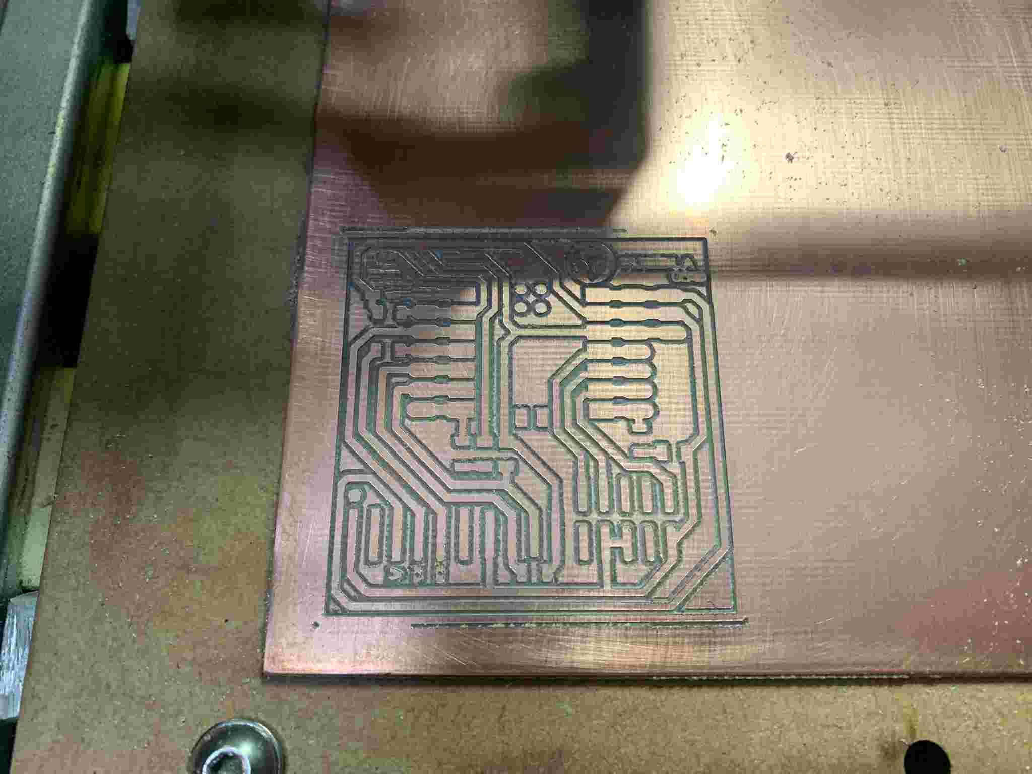
The milling process should take somewhere from 10 to 15 minutes, and the finished pattern should look something like this:
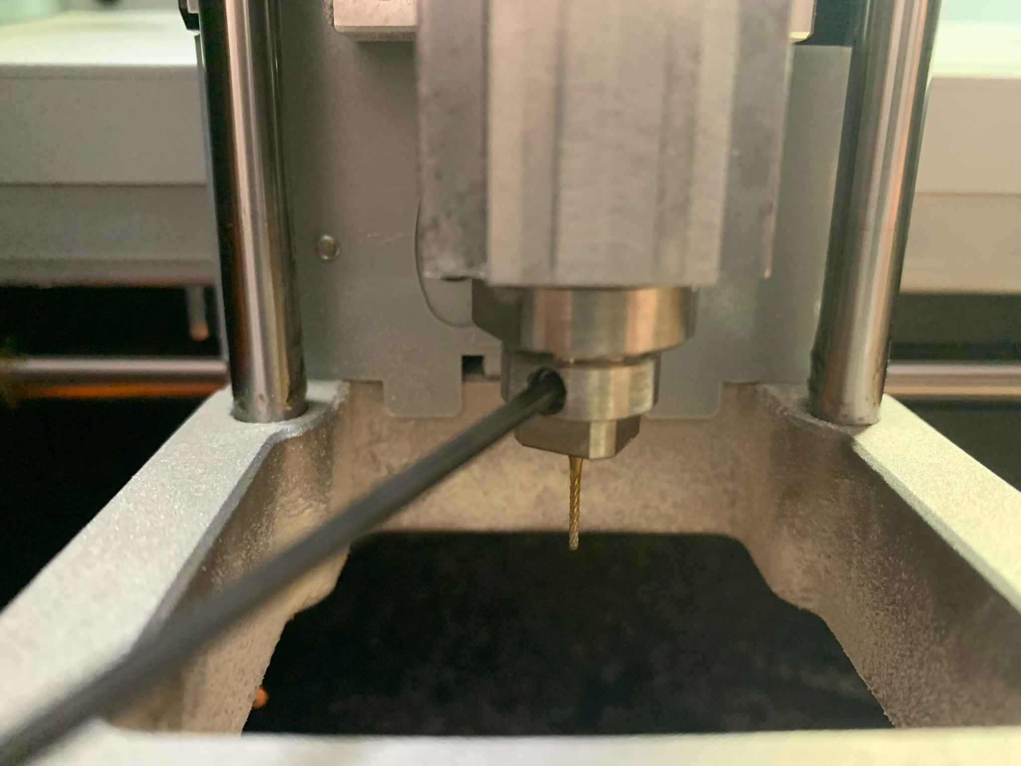
Once the milling is done, we have to change the tool on the machine's head, from the V-Cutter bit to the cutting drill bit. To do this you have to free the screw shown on the image below with a hex screwdriver. The bit should fall right off, but be careful with not letting it fall hard onto the bed, as the sharp edge may get blunt with the impact. Then, install the new bit by doing the opposite and tightening the screw, in the image, the new tool is already being installed.
Now, go back to the computer and return the machine's head onto the previously configured X/Y origin by clicking on the button circled by the blue line:
It is very important that you do not lose the intially set origin point, as making that the board's outline cut and the inside's pattern coincide, can be very difficult!
Now lower the new tool by using the same paper technique we used before. Once this is done you can import the cutting outline's G-Code file and start a new cut. This may take another 5 to 10 minutes. When it is finished, you should have your PCB as a separate piece that you can take off the MDF board. The result should look something like this!
Soldering Components!
Now onto the most delicate part: Soldering the components onto the board, so it actually does something.
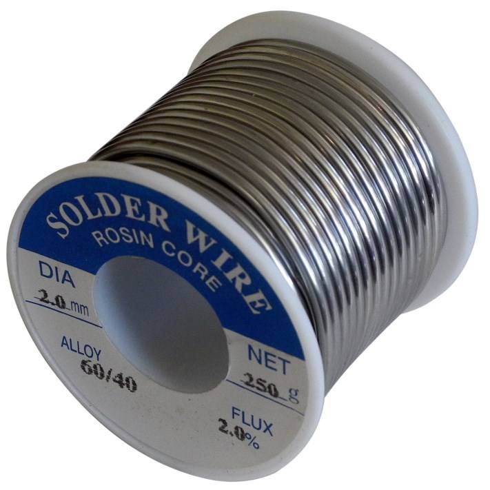
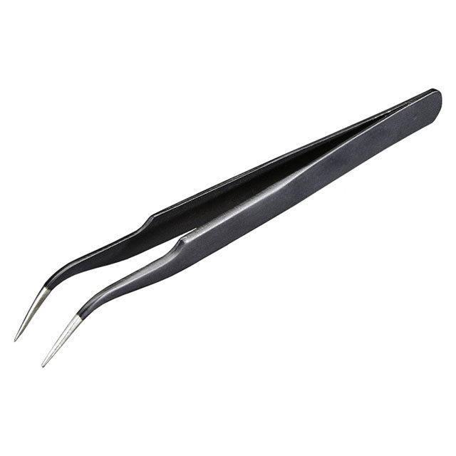
To do this you'll need: A soldering iron with a fine tip, 60/40 tin solder wire, and a pair of delicate tweezers. Just like the ones below.
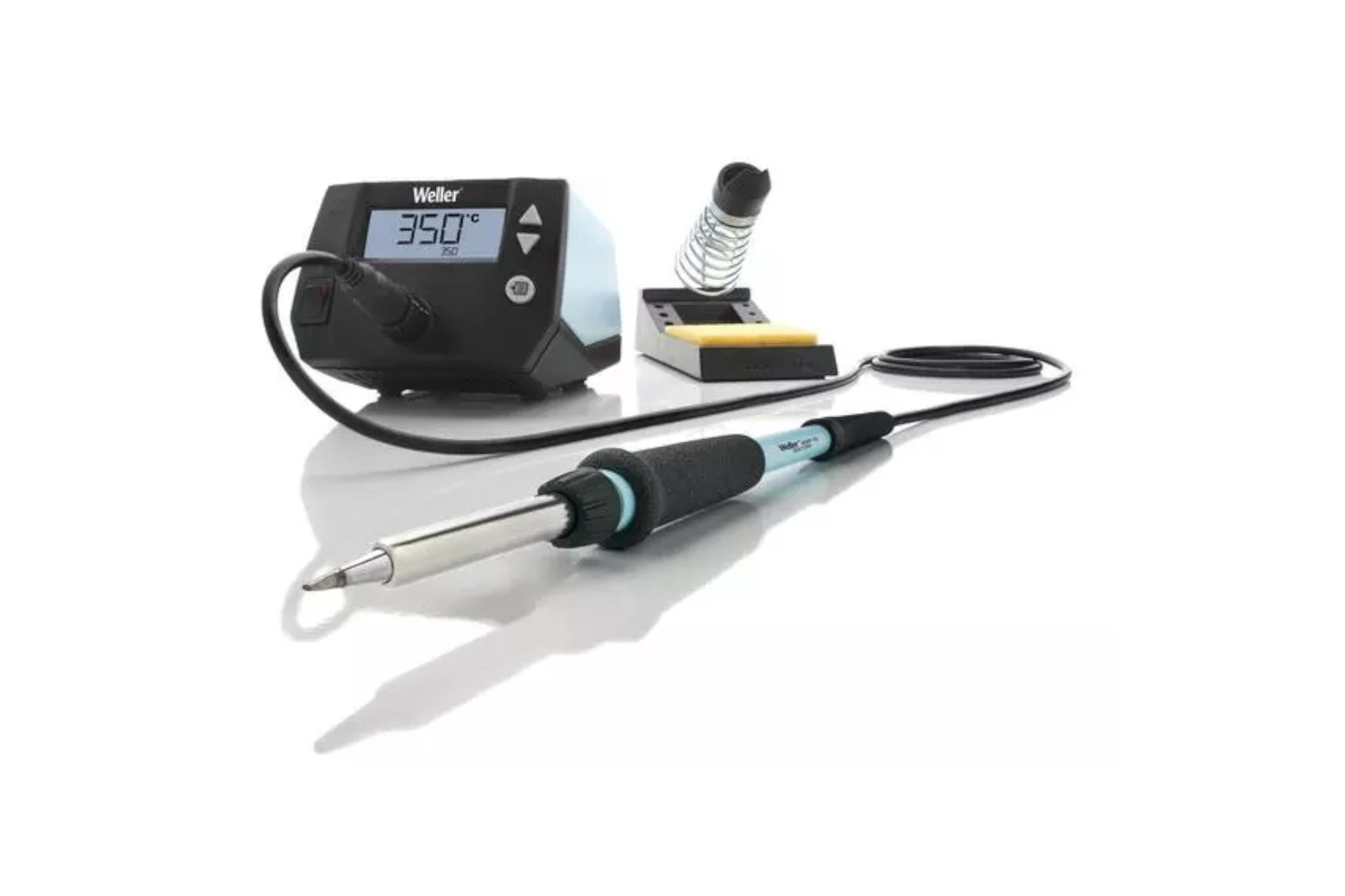
Set the soldering iron's temperature to about 100°C above the melting point of the 60/40 solder alloy, which is about 180°C, by doing this you ensure the solder is liquid enough to be workable, but not hot enough to damage the components you are soldering.
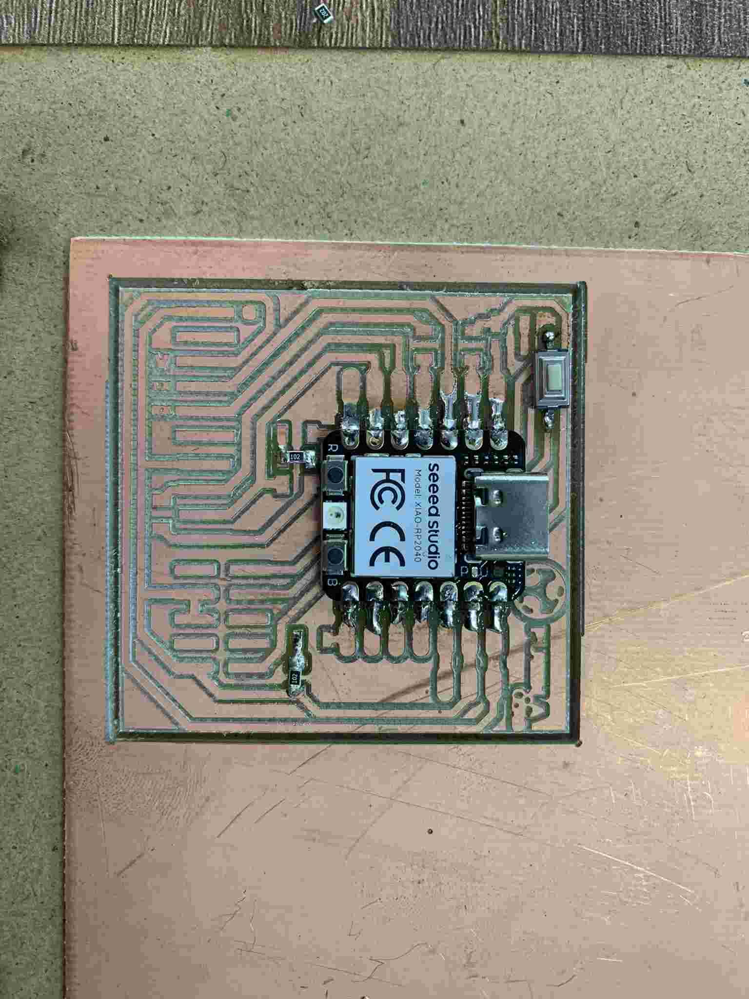
When soldering this board I suggest you start with the XIAO RP2040 module, as it has the biggest solder joints in the whole board. If you start by soldering smaller pieces, the heat conducted by the board's copper traces might melt surrounding solder joints, potentially ruining your work. This is specially true if you have little experience soldering and tend to overheat the solder joints!
In this image I soldered first the XIAO module, and then adjacent smaller components, such as the two little 1kOhm resistors and a pushbutton on the top right. To solder the smaller SMD components you will certainly need the fine tweezers, as they will help to hold the component with precision and without getting your fingers burned.
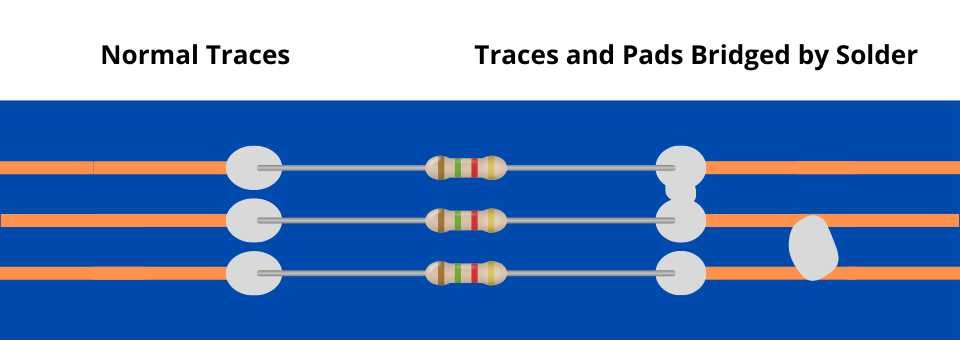
When soldering, the result should be a shiny round solder point, or a shape that adapts nicely onto the copper pads and the component's metal pins. If the solder point seems opaque, cracked or not smooth at all, that joint may not be doing a good connection and will fail soon, or not work at all. As there's no solder mask on this PCB, the solder joints may get bigger than needed. As long the recommendations above are followed, this shouldn't pose a problem beyond aesthetic considerations.
Another thing to look for when soldering components, specially when working on pads very close to each other or soldering on bare copper PCB's (such as this one) is bridging. Bridging is when you, accidentaly, connect two or more points of the circuit with solder that were not meant to be connected, and turning on your circuit with this problem unresolved may cause from simple malfunctions, to a short circuit that damages everything on the board. So, look out for them! Using a magnifying glass or microscope, identifying those solder bridges should be pretty easy.
If you find one of those bridges, don't panic!, just heat up the solder joint and, give it a little smack onto the table or use a desoldering pump, the excess solder will fall, leaving behind the individual connections. Just re-apply solder to make sure each connection is well done.
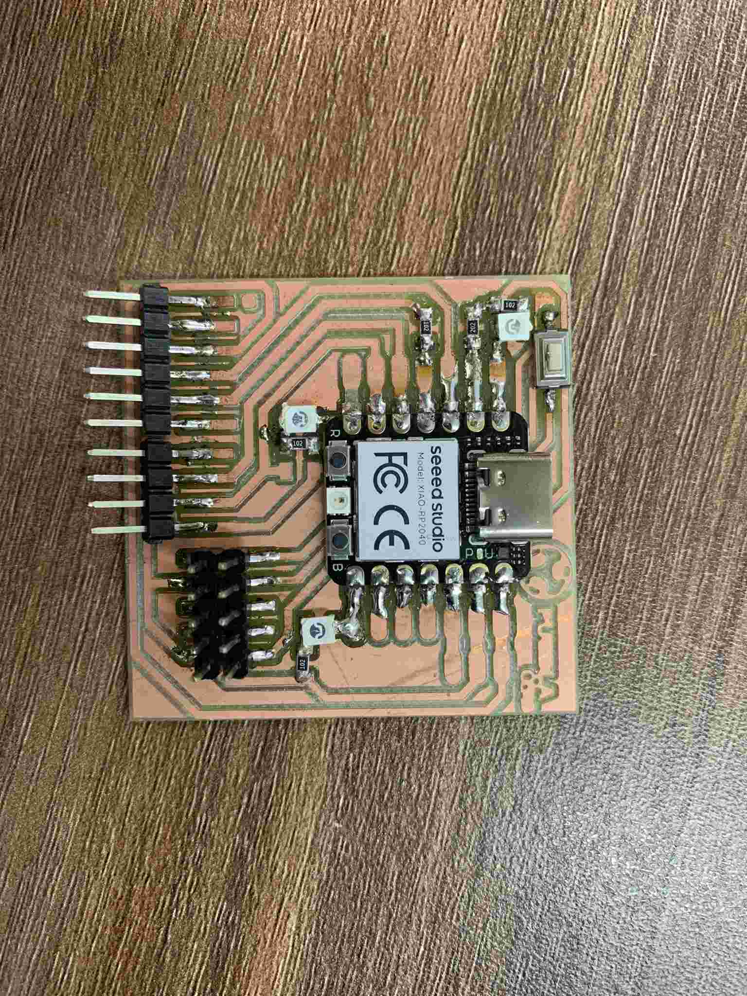
Once you have finished soldering all the components onto the board, and have checked for bridges and bad solder joints, your board should look just like this:
And now it's time to test it!
To do this we have to upload a simple code which will make the two bottom LED's blink every second, and the top LED blink every second while the button is pressed. To upload the code we have to install the latest version of the Arduino IDE, a code editor and programmer meant for microcontrollers and other kinds of embedded devices.
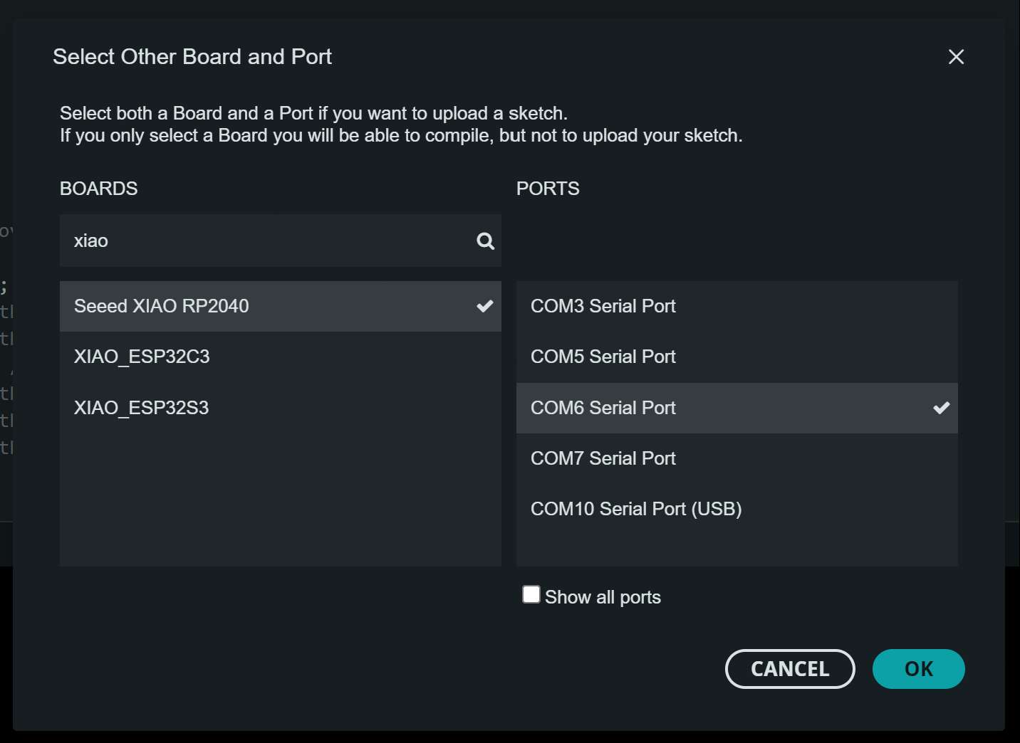
The XIAO RP2040 board is not installed by default onto the Arduino IDE, but doing so is very easy:
Open your Arduino IDE and go to File -> Preferences (Or press Ctrl + ; on the keyboard) and this window will open:
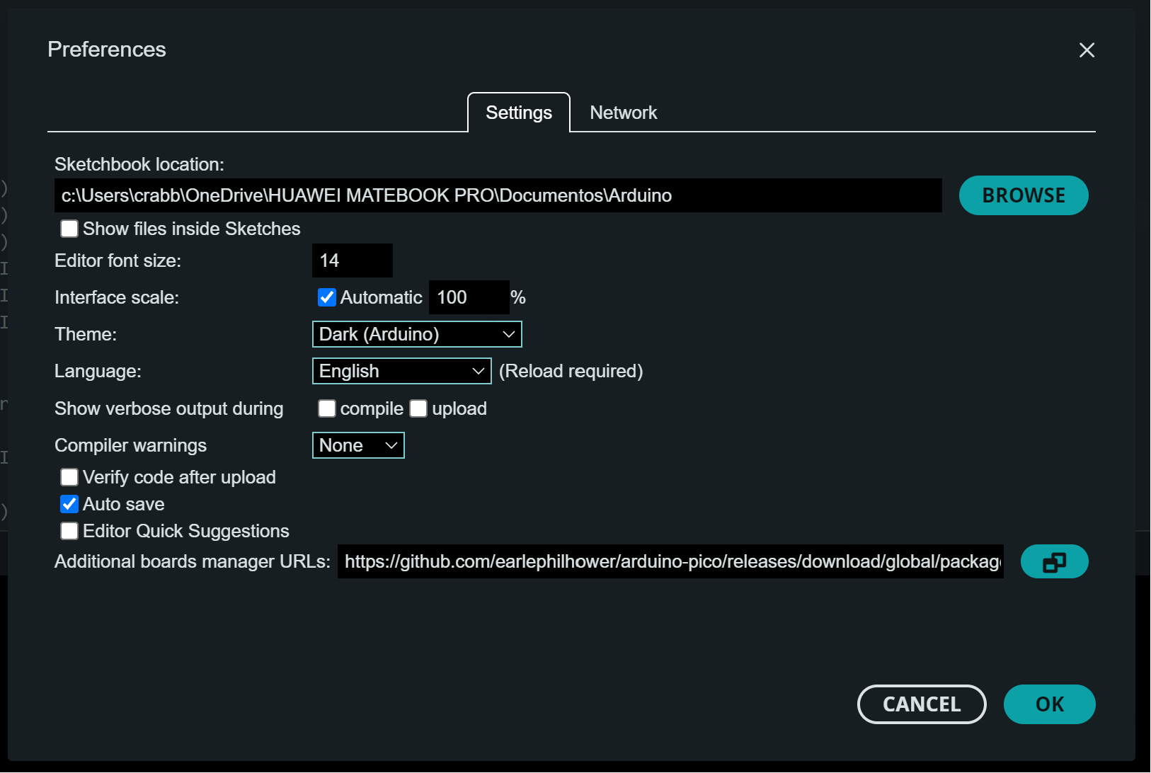
Inside the textbox with the legend "Additional boards manager URL's" copy and paste this URL:
https://github.com/earlephilhower/arduino-pico/releases/download/global/package_rp2040_index.json
Now you can close this window and the installation of all the needed files to program the XIAO board will be installed automatically. This process may take a while depending on your internet speed.
Once the board dependencies are installed, you can connect it to your computer using a Type-C USB cable. When doing so the XIAO module on the PCB should light right up, if that is not the case, disconnect it inmediately and check your solder joints for any possible errors.
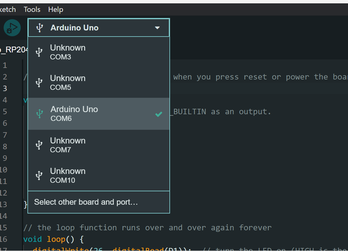
If the board is up and running, we can look for it on the available serial ports, in my case it shows up in the COM6 serial port. Select the port, look for the board on the searchbox and click on it when you find it. Now download the code from the links at the end of this page and open the .ino file.
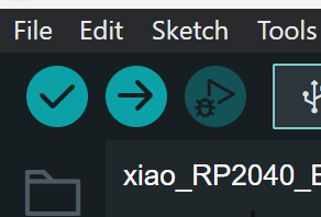
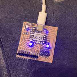
If you have done all of this, you can click "Upload" (Circle with arrow) and enjoy the magic! The leds on the PCB should start blinking, meaning we have sucessfully fabricated our own PCB!
Thank you for taking a look into my 4th week's progress!