Week 8: Electronics Production
Overview
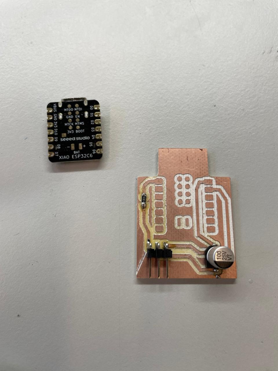
This week, I transformed my crystal holder deadbug prototype into a real, grown-up PCB using KiCad and a Roland SRM-20. It’s now clean, sturdy, and surprisingly still functional. No more floating wires and taped-on dreams.
Checklist
Group Assignment: Understanding the PCB Production Workflow
As a group, we explored the full workflow of PCB fabrication—both in-house and outsourced. We compared the benefits and constraints of using the Roland SRM-20 milling machine versus ordering boards from a fabrication house. We also:
- Learned about milling tools and the types of bits required for different tasks (traces vs cutouts).
- Used MODS CE to generate toolpaths for the SRM-20.
- Reviewed techniques for double-sided PCBs and layer alignment.
- Discussed soldering techniques and board cleaning post-fabrication.
- Compared local production vs. sending files to a boardhouse (cost, lead time, design rules, file formats).
Findings: We learned that while in-house milling is faster and great for prototyping, it lacks the precision and durability of professionally manufactured boards. Tool selection and MODS CE settings play a major role in determining quality, and double-checking everything (especially toolpaths) saves you from rerunning jobs. Overall, it was a valuable crash course on what it means to take an idea from schematic to physical board.
More details on the group page: FabAcademy Puebla - Week 8
Tools & Software
| Tool | Logo | Description | Specs | Link |
|---|---|---|---|---|
| KiCad | PCB design software | Open-source, Gerber + SVG export | KiCad | |
| MODS CE |  |
Toolpath generator for PCB milling | Outputs Roland-compatible .rml files | Mods |
| Roland SRM-20 |  |
PCB milling machine | 0.2mm V-bit, supports RML | Roland SRM-20 |
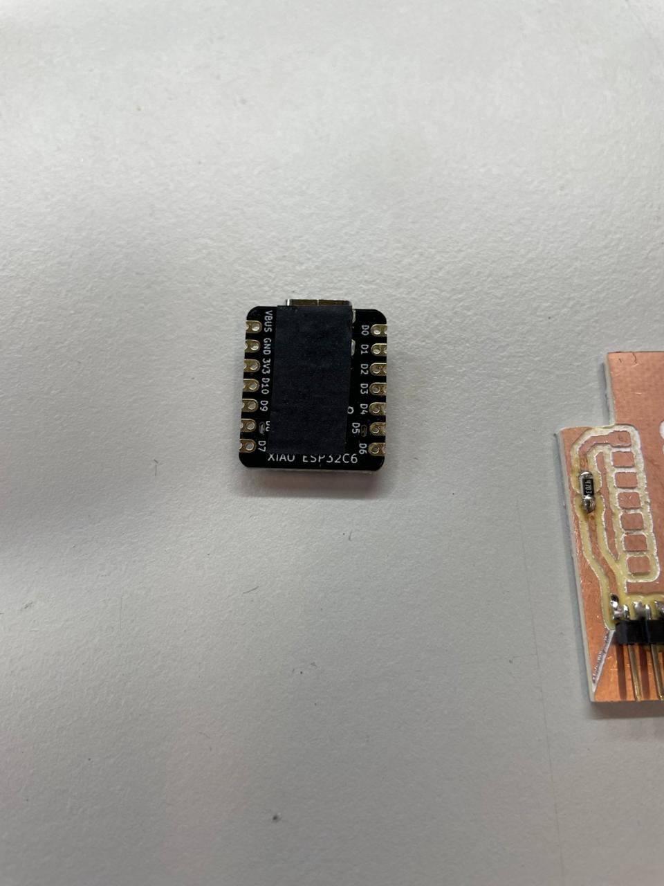
| XIAO ESP32C6 | 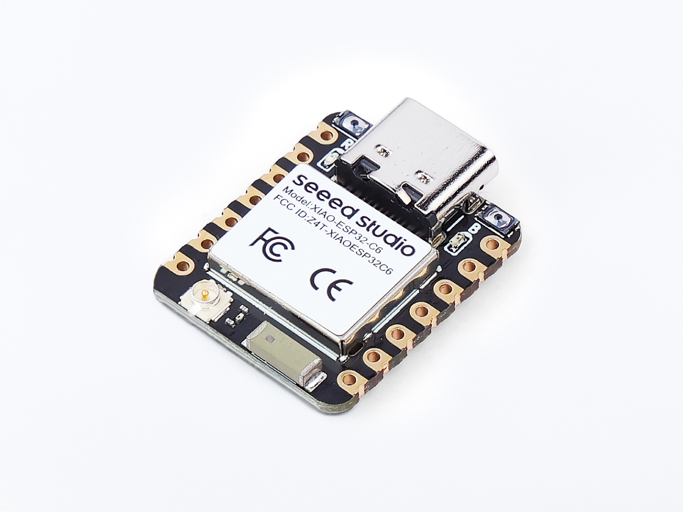 |
Microcontroller | WiFi + BLE, USB-C, low power | XIAO ESP32C6 |
Making the Toolpath
First, I made my schematic. It is an improvement and a simple version from Week 6.
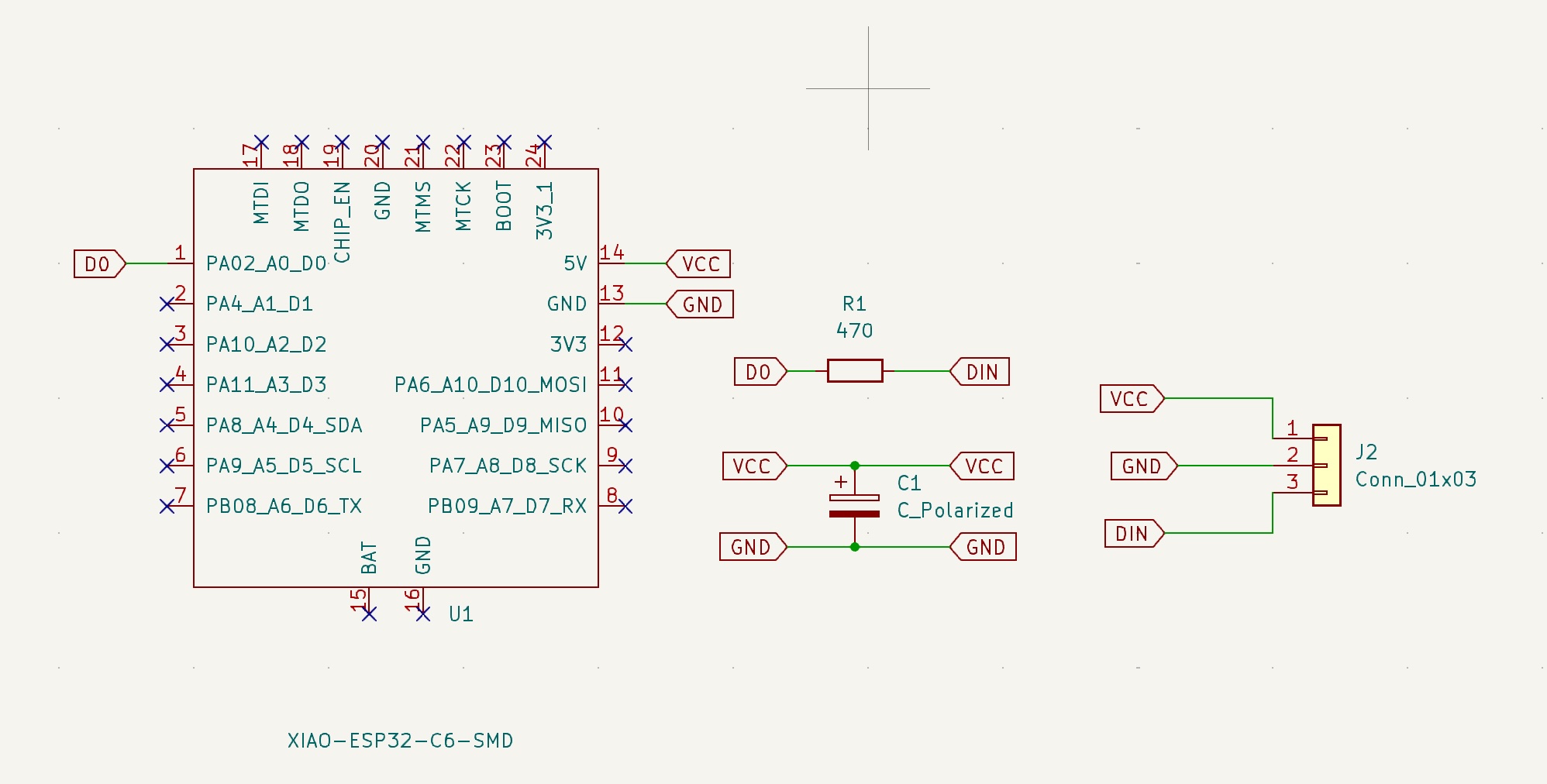
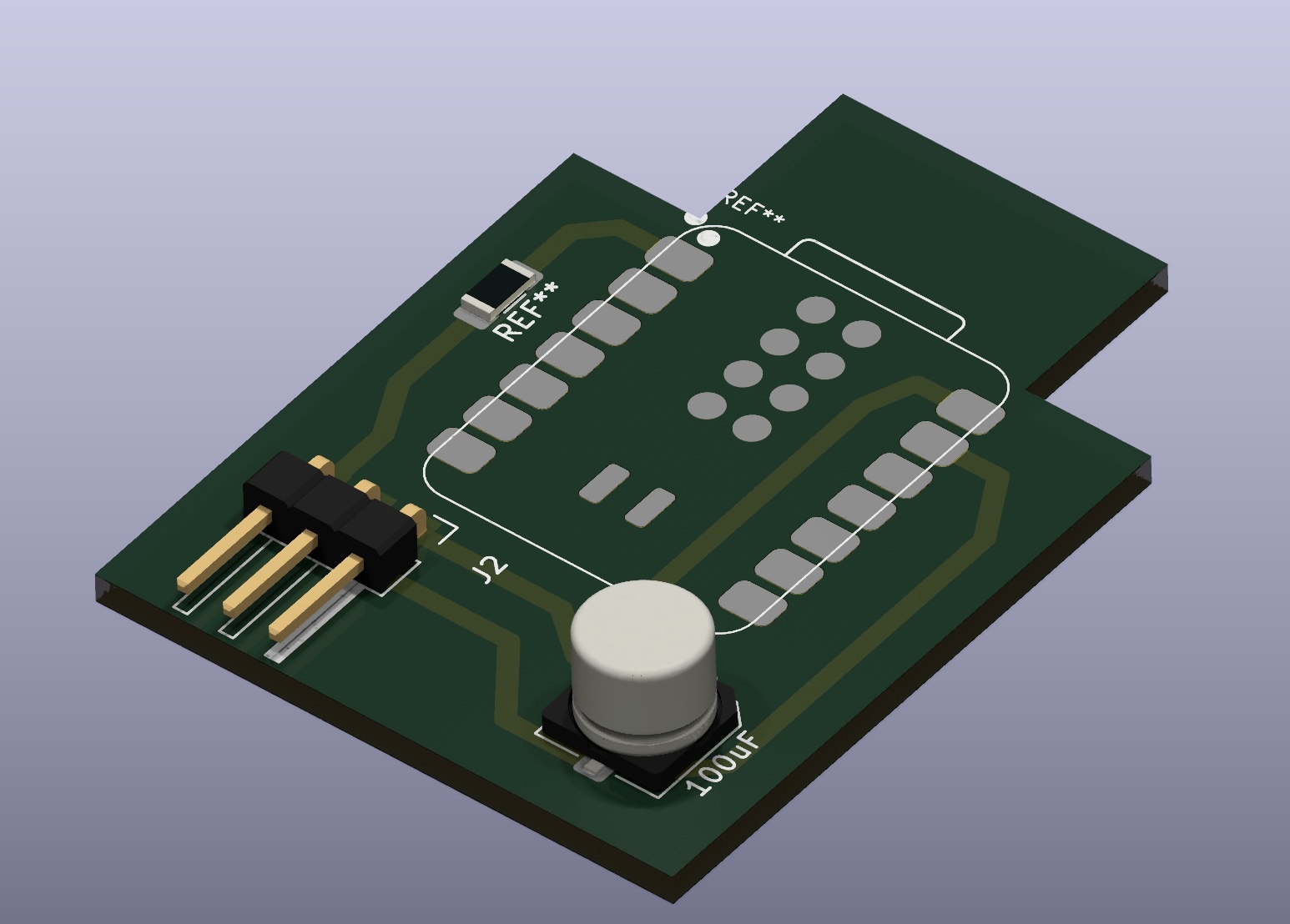
Then I went to the PCB editor to connect the ESP32C6 to the resistor, capacitor, and to the 3-pin header. Then I drew the edge and placed it on the Edge.Cuts layer. Then I generated the 3D render of the PCB.
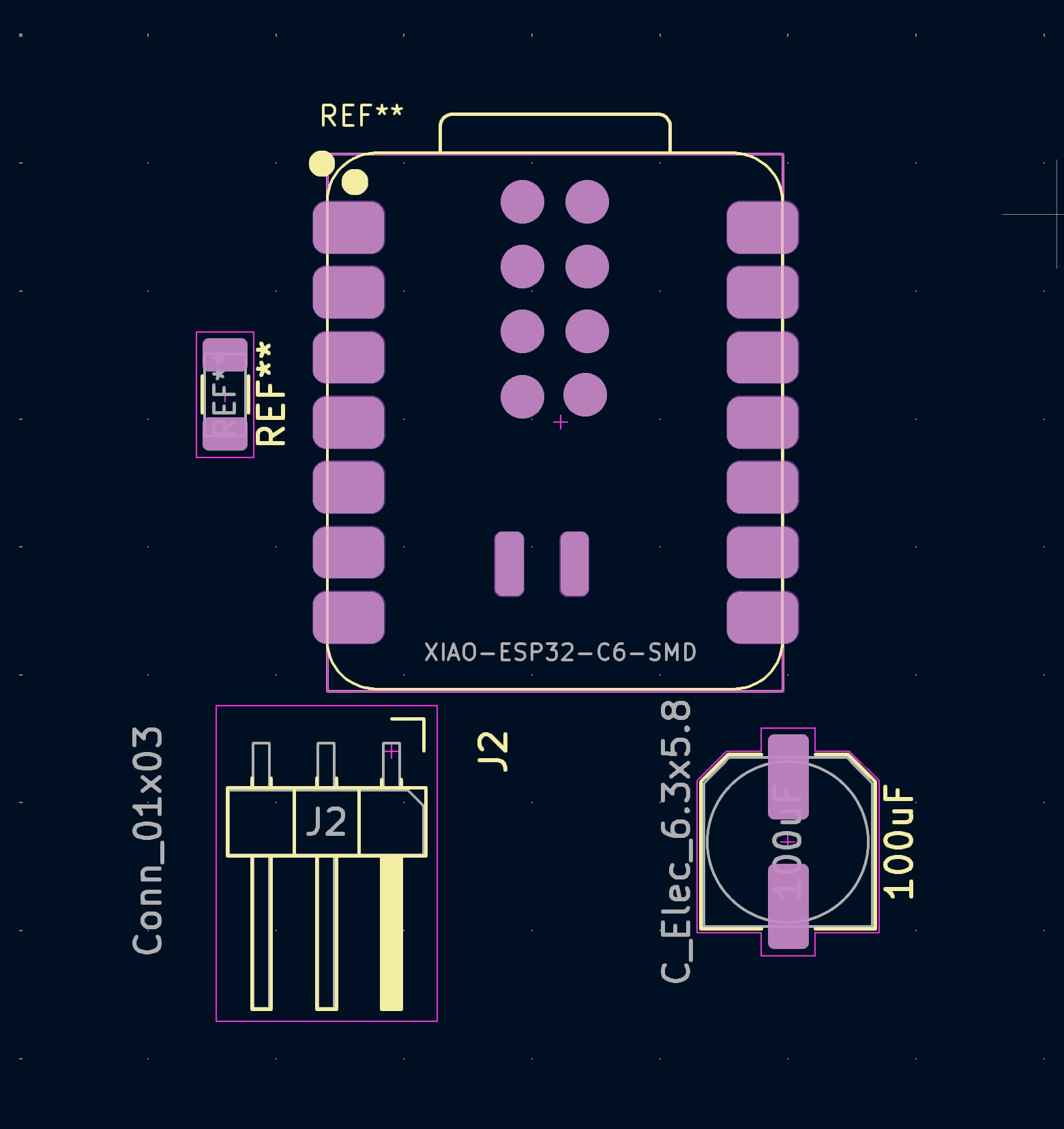
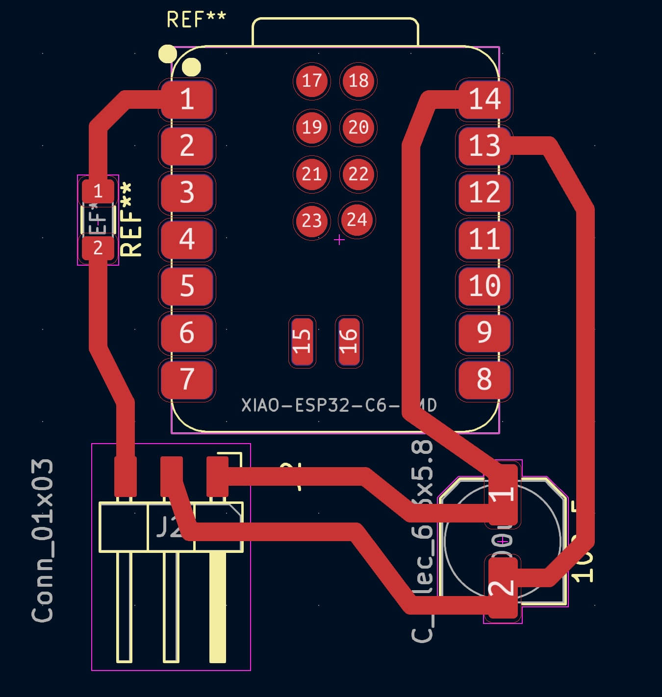
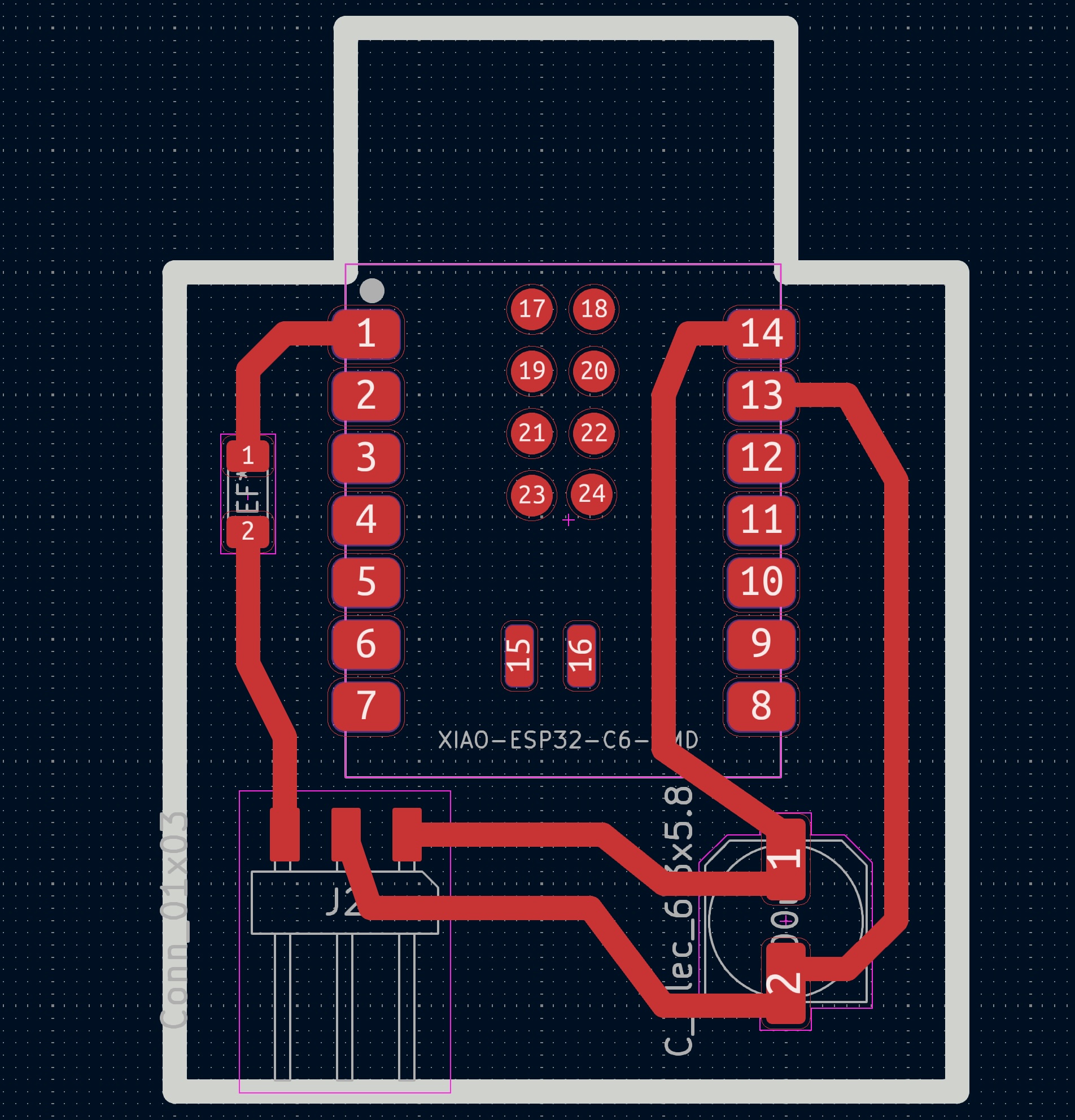
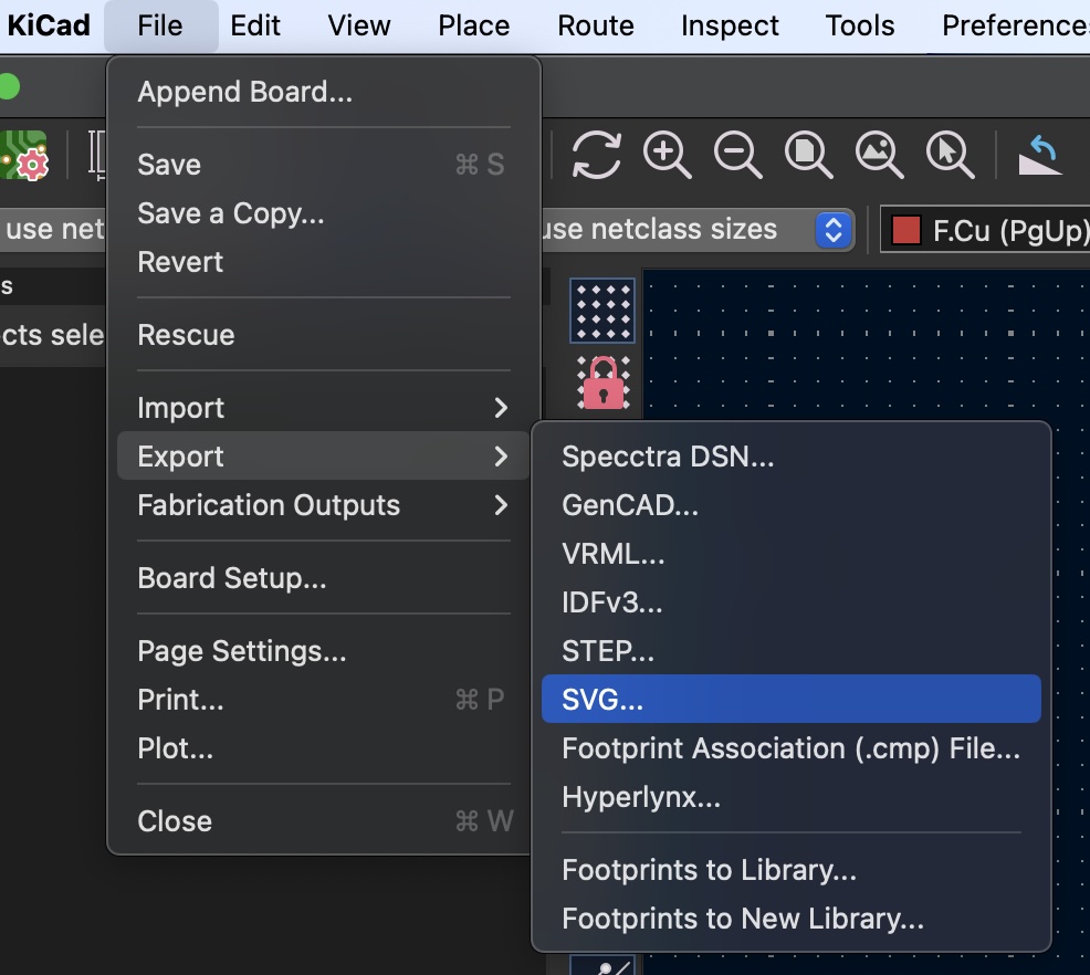
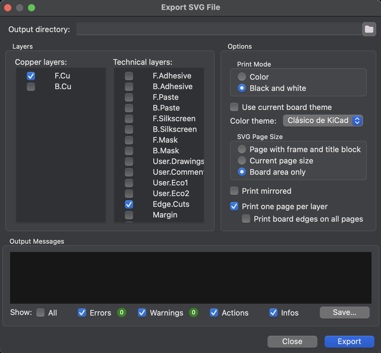
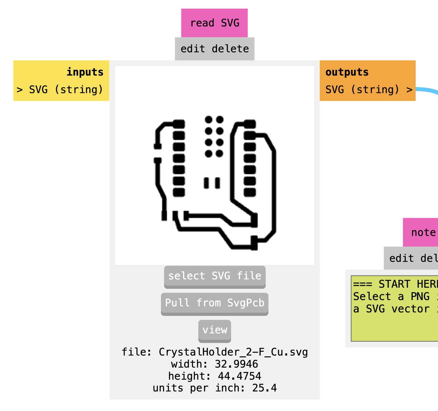
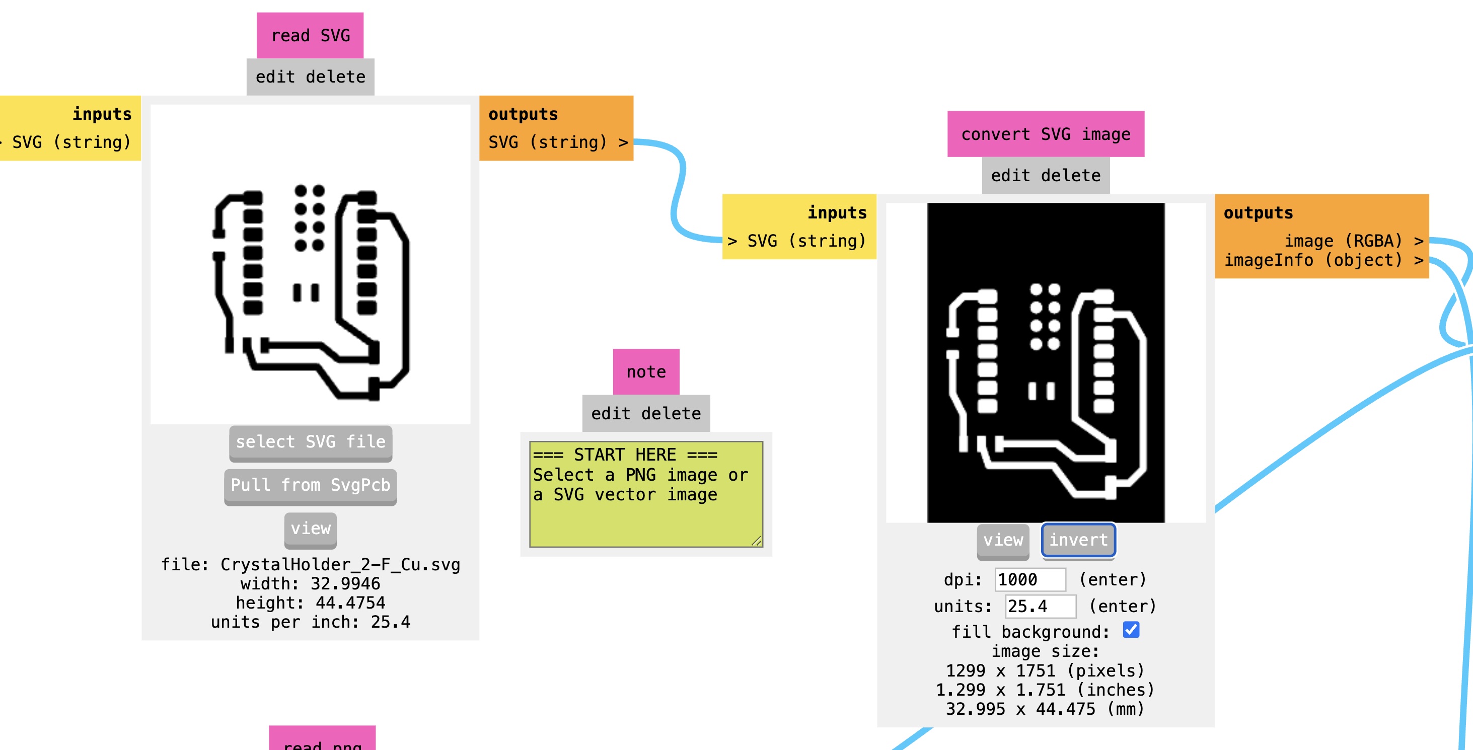
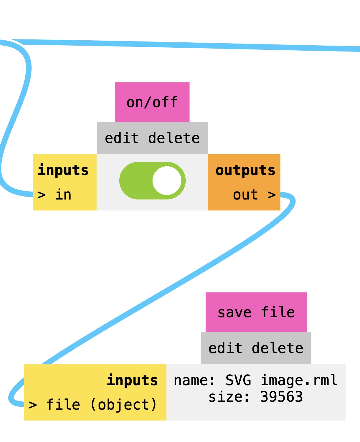
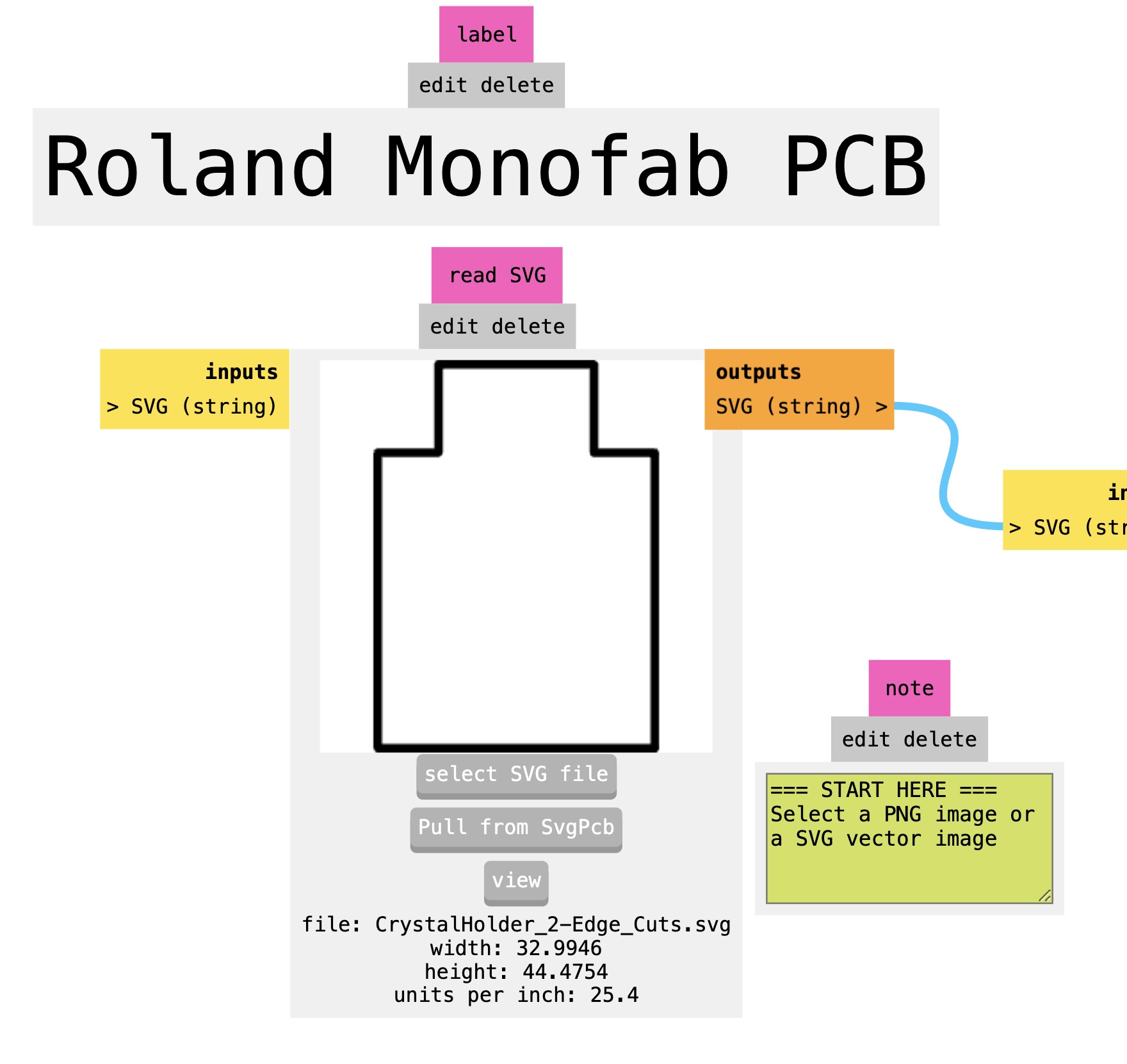
I exported the SVG file. I selected the layers I needed for this PCB. So it exported two SVG files: one for traces (copper layers) and one for the edge (Edge.Cuts layer).
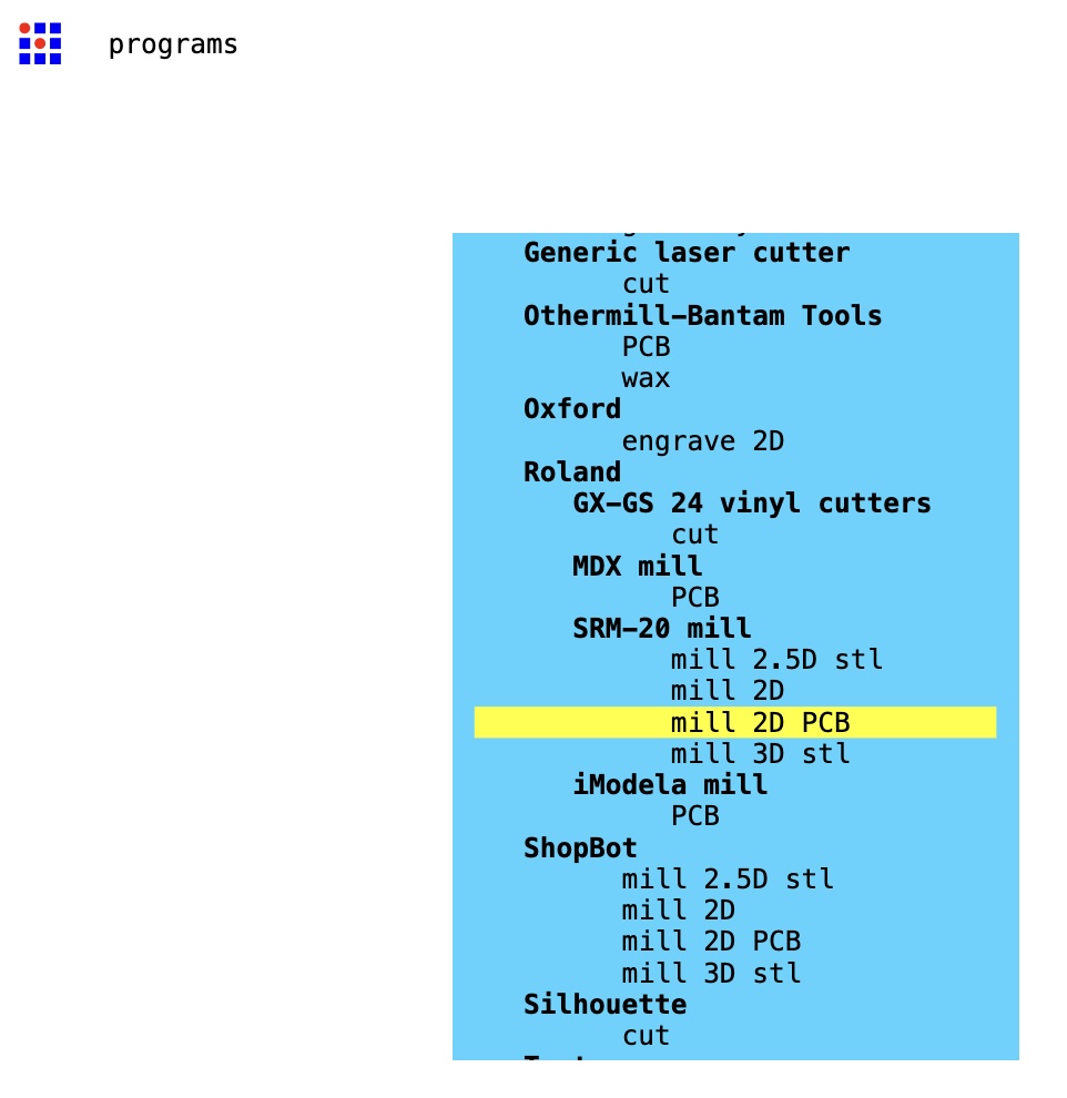
Then I went to MODS. Right click and a menu appears. Select 'programs', then 'open program', and scroll down to Roland SRM-20 mill and select 'mill 2D PCB'. Then you get strange-looking boxes with blue connectors. It is a strange UI but it works like a charm.
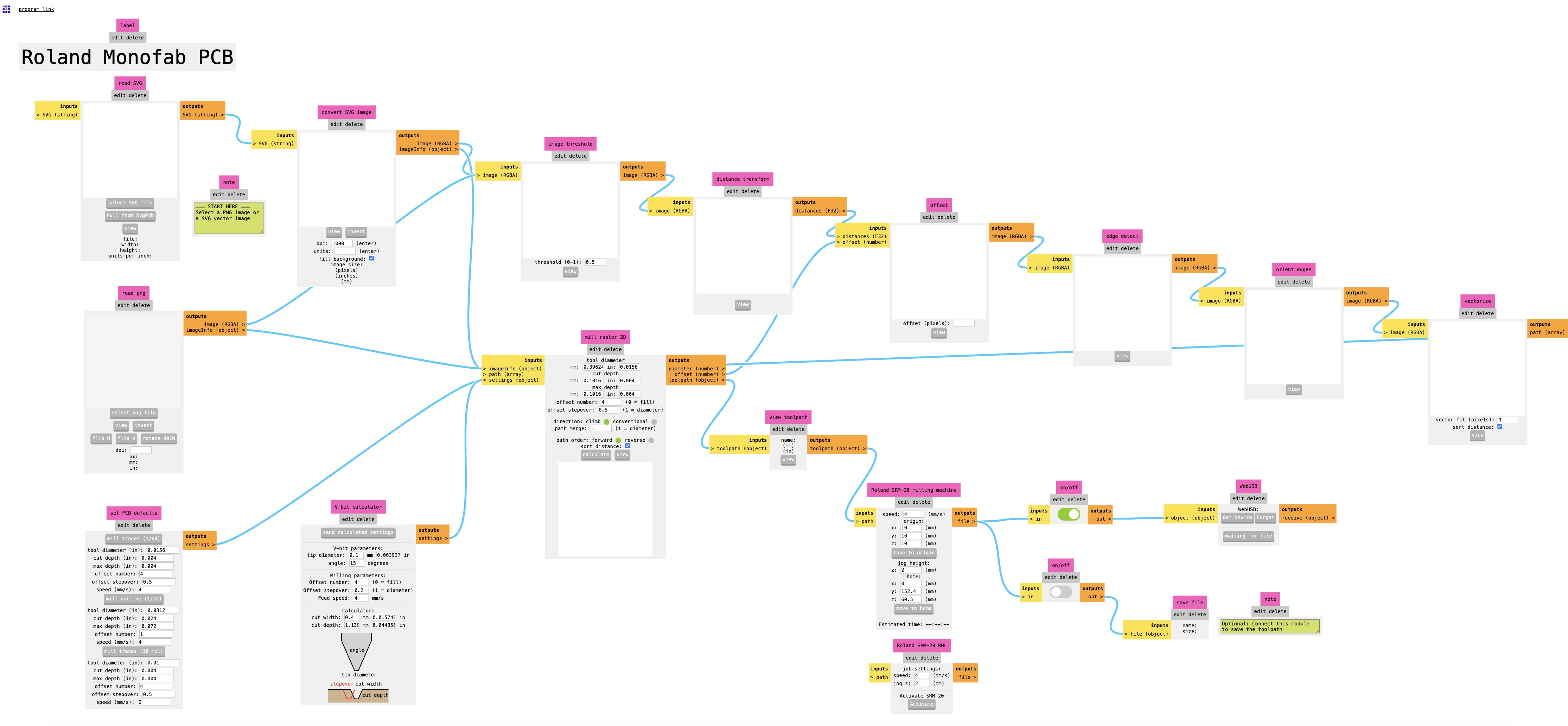
Once in MODS UI I did the following:
- Uploaded the SVG file
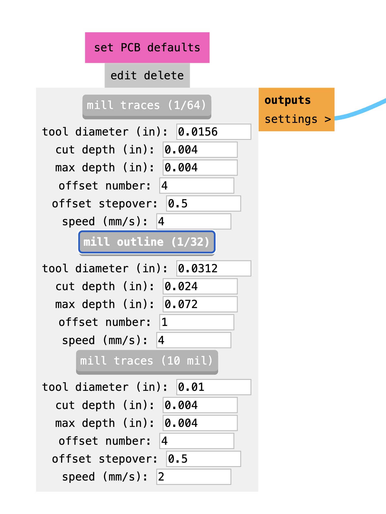
- Set tool preferences to mill traces
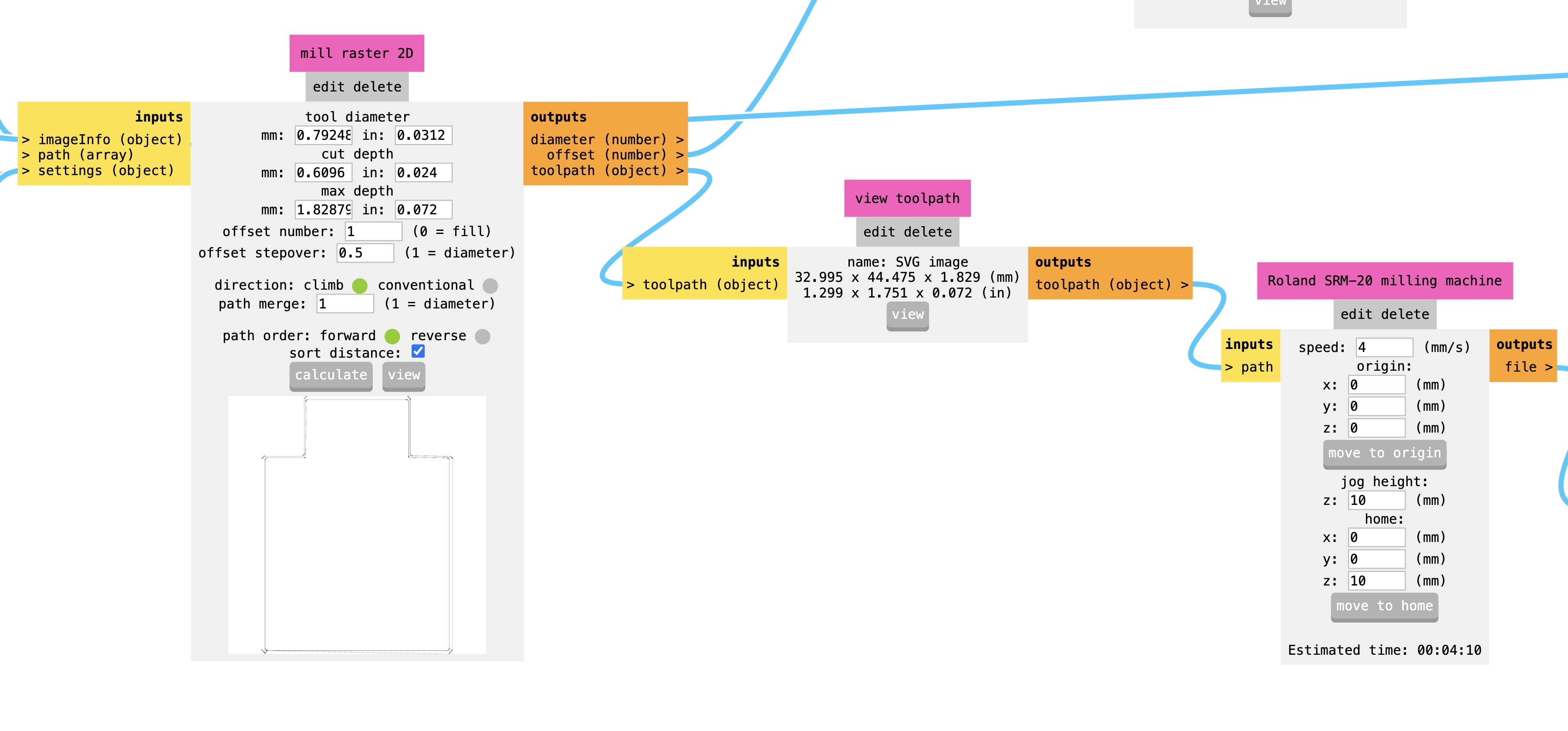
- Sent the calculated settings to the mill raster
- Parallel to this, I inverted the SVG image so it only cuts the traces. How do I know this, you ask? Well... I didn’t do it like that and the Roland mill cut just the traces, like a negative—and that of course did not work. Big mistake, great learning.
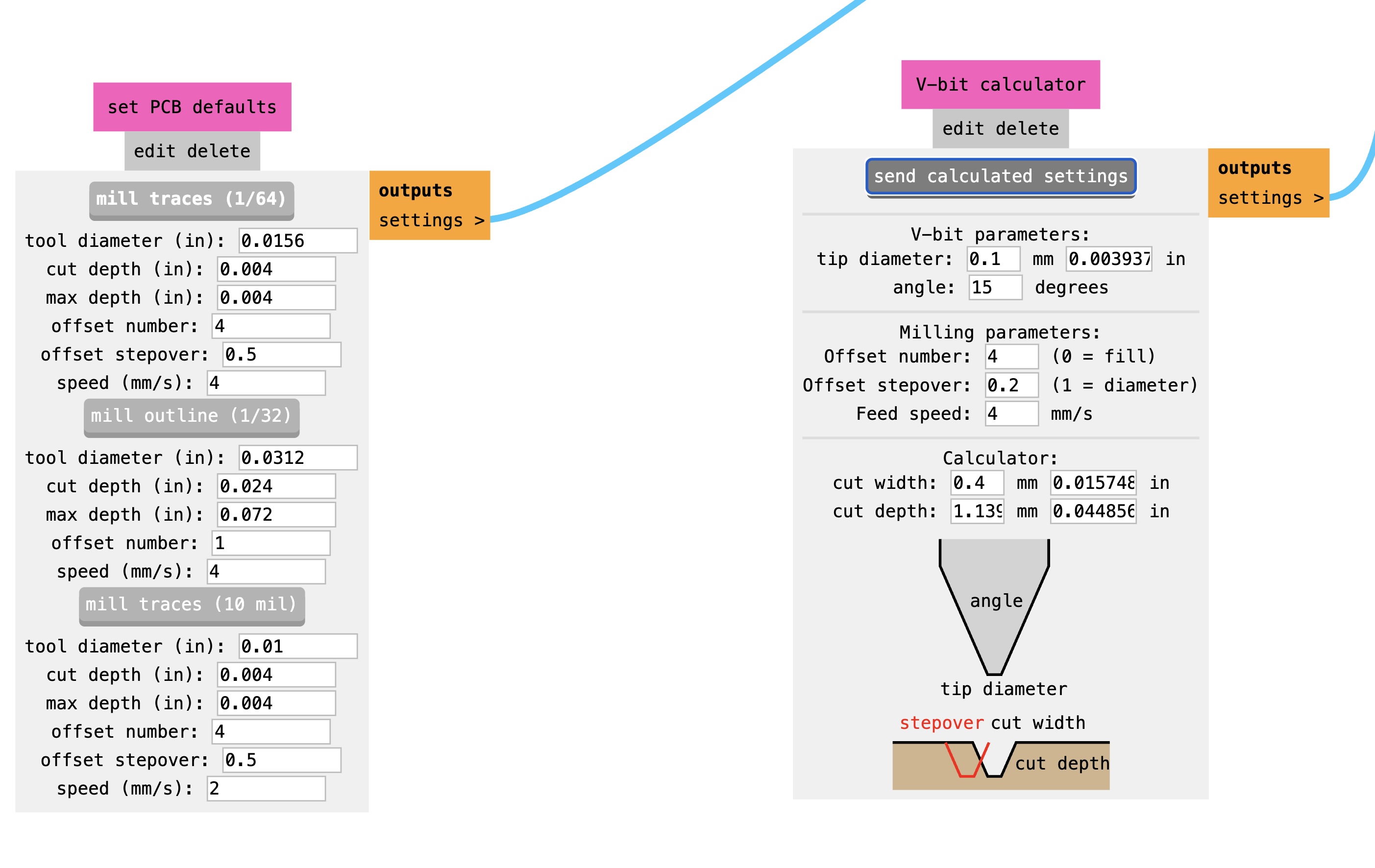
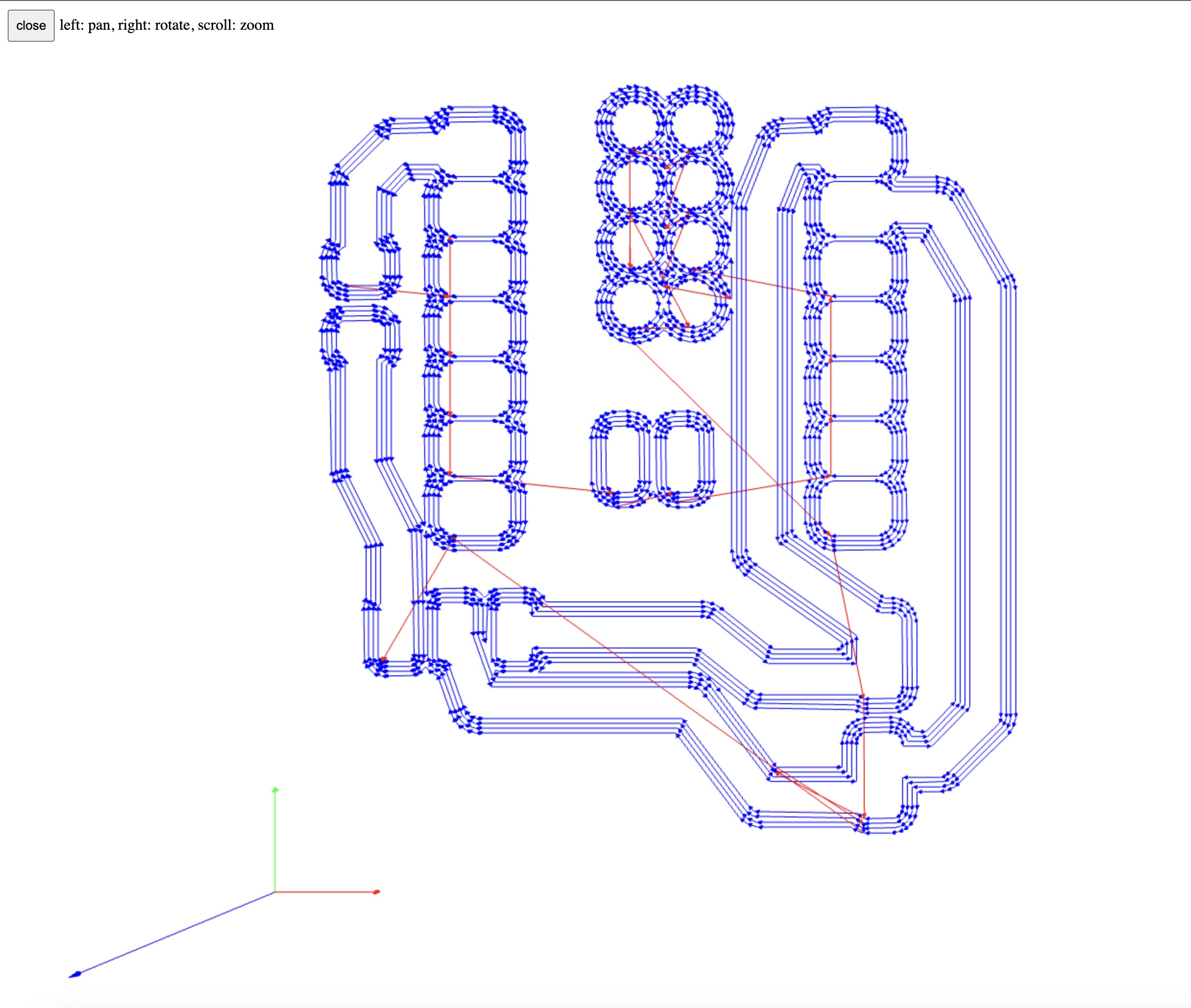
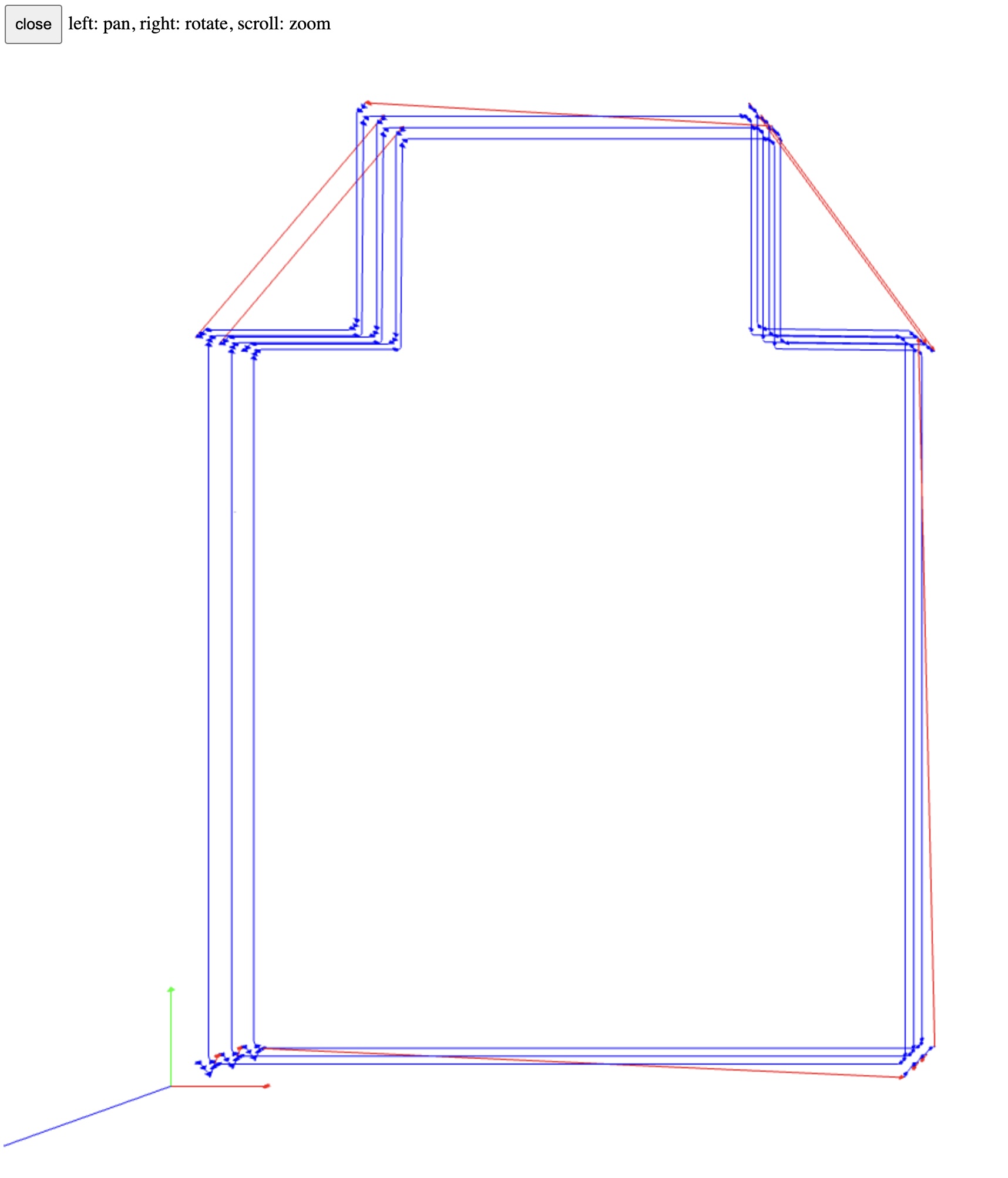
After that, I calculated the time and toolpath with the raster mill and it gave me a good-looking toolpath.
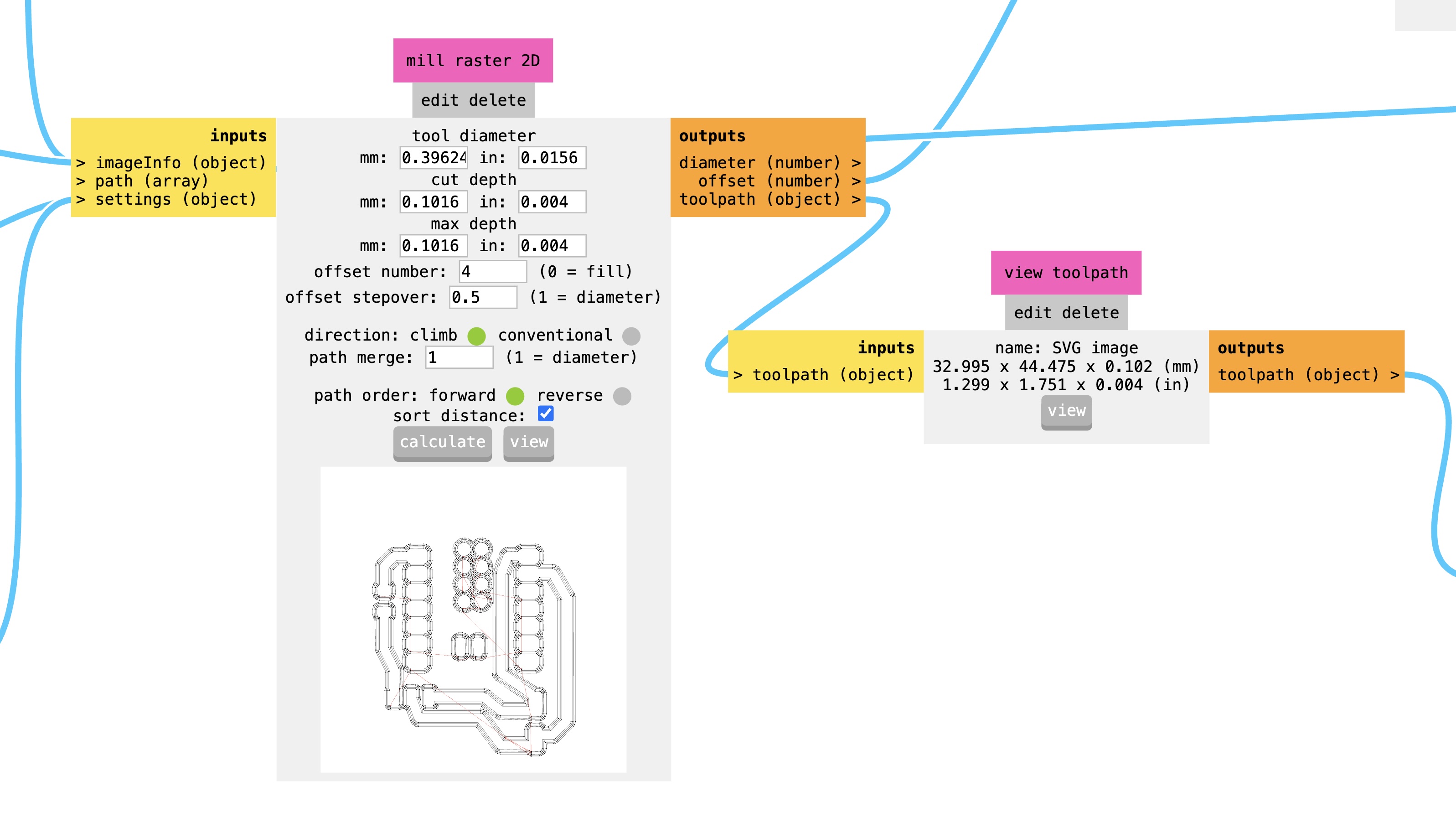
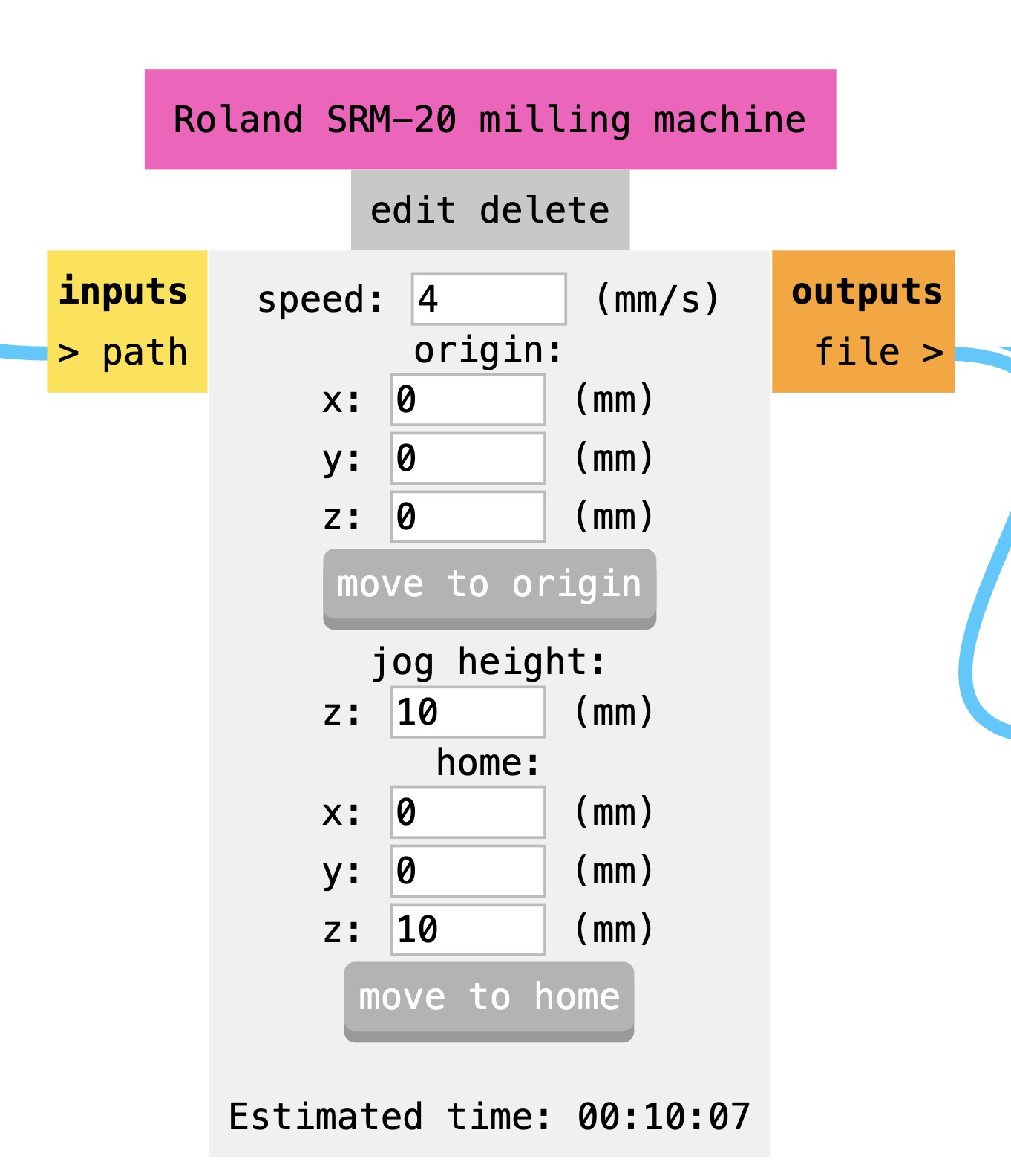
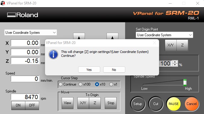
But that is not all. I needed to change some milling machine settings, so I placed the origin in zero (X, Y, and Z). But another mistake was made here—I placed all in zero. That meant that when the tool changed or moved, it was going to be too close to the board and might scratch it. Also, and this happened, I placed the final cut again in zero so it made a scratch on my board. Fortunately, it didn’t affect it this time, but that needs to be corrected in future mills. Just change jog height and Z in home, and that will do it. Have in mind that higher jog height might incur in more machining time.
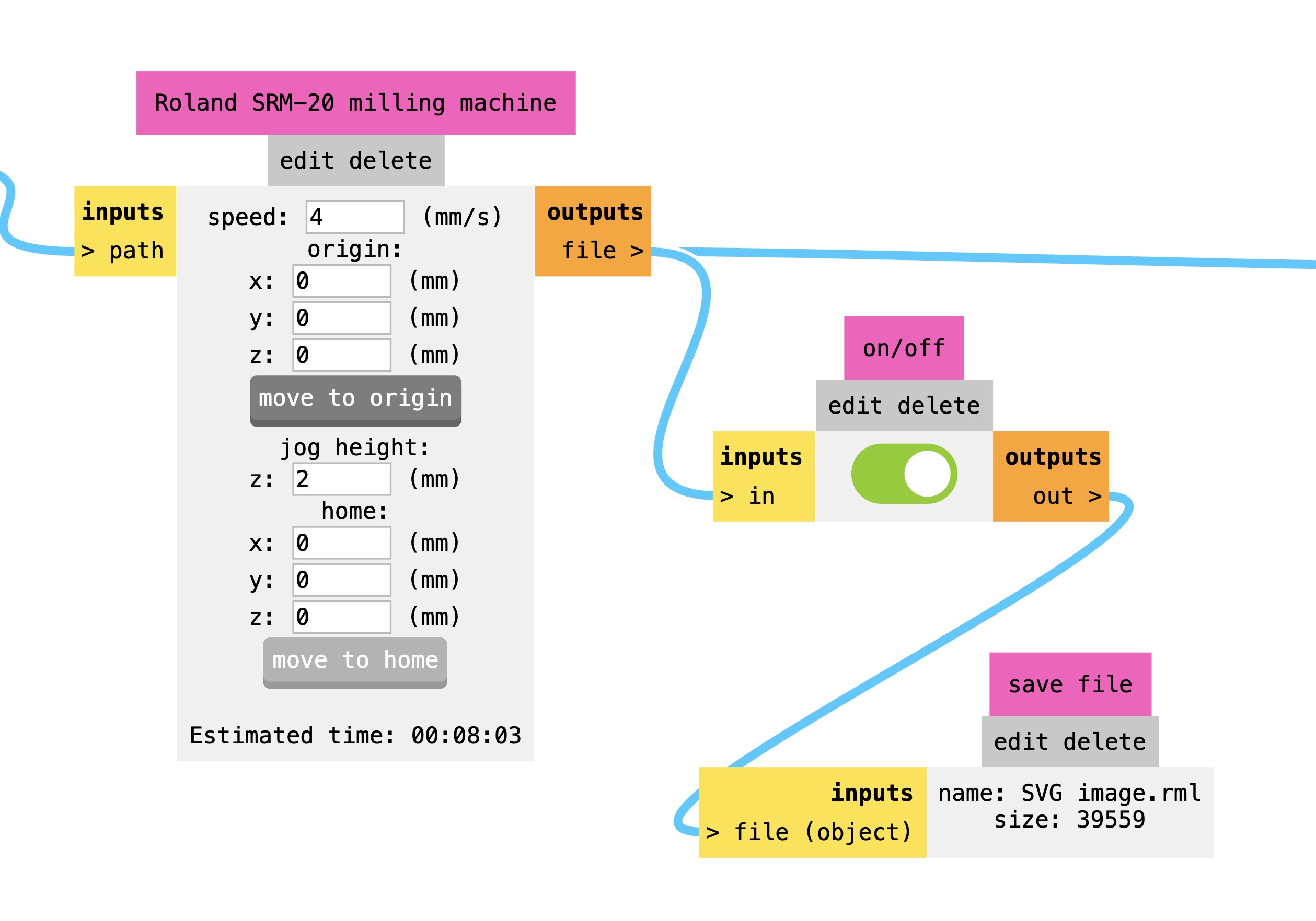
Finally, turn on the RML file output so you can download the file to put on the Roland SRM-20.
The edge cut was done using the same procedure as the traces, with two important changes. This time, I did not need to invert the SVG. Also, instead of selecting mill traces, I selected mill outline. I kept the same jog and home height settings to ensure a clean, safe cut — and yes, this time it didn’t scratch my board.
Fabrication: Milling, Stuffing, and Soldering
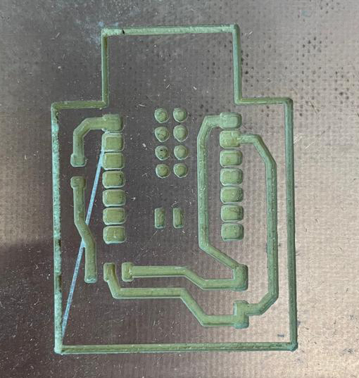
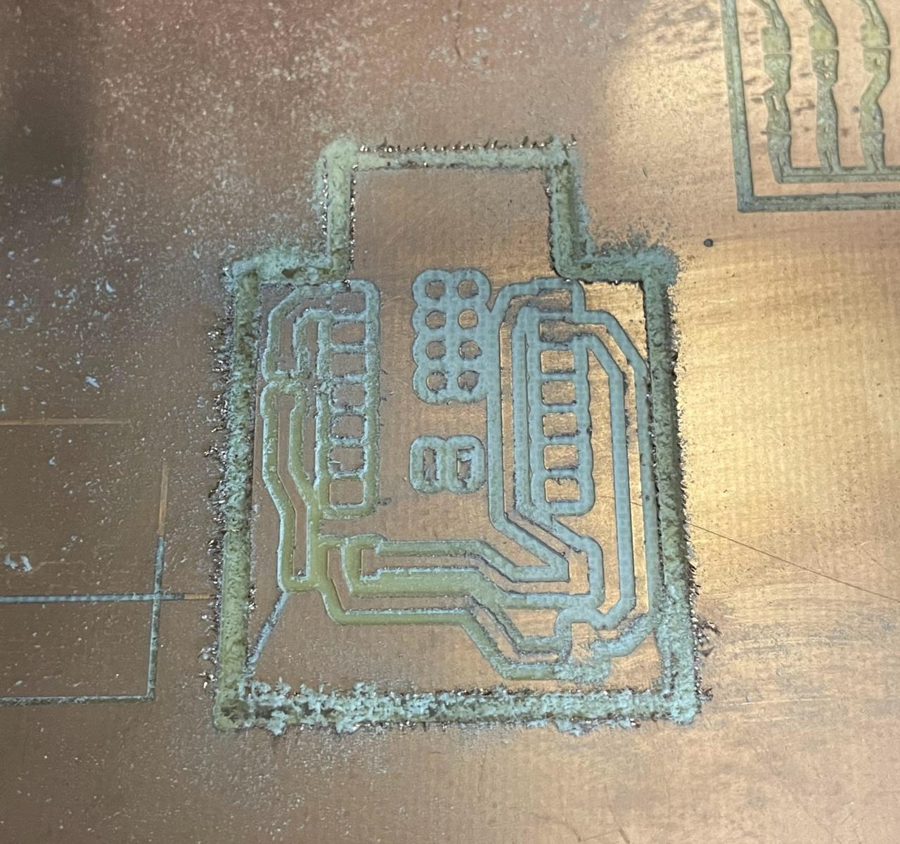
I mounted the blank PCB on the Roland SRM-20 with double-sided tape (because nothing says "high-tech" like arts and crafts supplies). First, I milled the traces—clean and satisfying. Then came the cutout pass.
Fabrication: Milling, Stuffing, and Soldering
First step: open the Roland software VPanel for SRM-20.
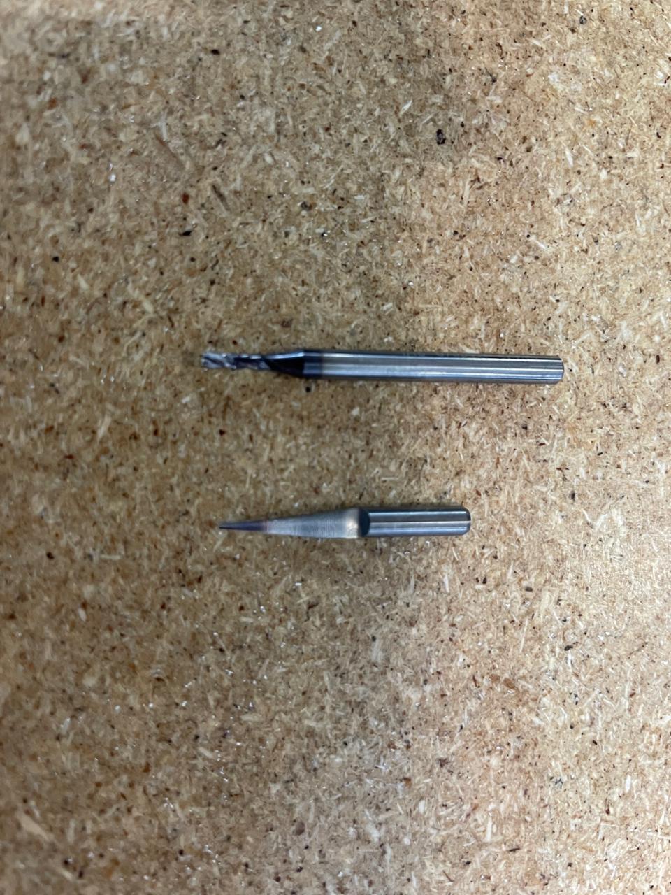
Select your cutter — a v-shape bit for traces and a flat mill for the edge cut. Carefully place the tool and adjust the height manually.
Again in the VPanel, set the coordinates to zero (X, Y, and Z) at the corner of your board. Then press the Cut button, add your toolpath file, press Output, and watch the magic go ✨.
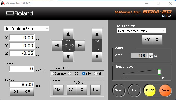
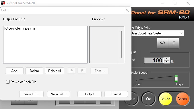
We repeat the same process for the edge cut — but this time, do not change X and Y coordinates. Only update the Z height, since the tool was replaced and the length is different.
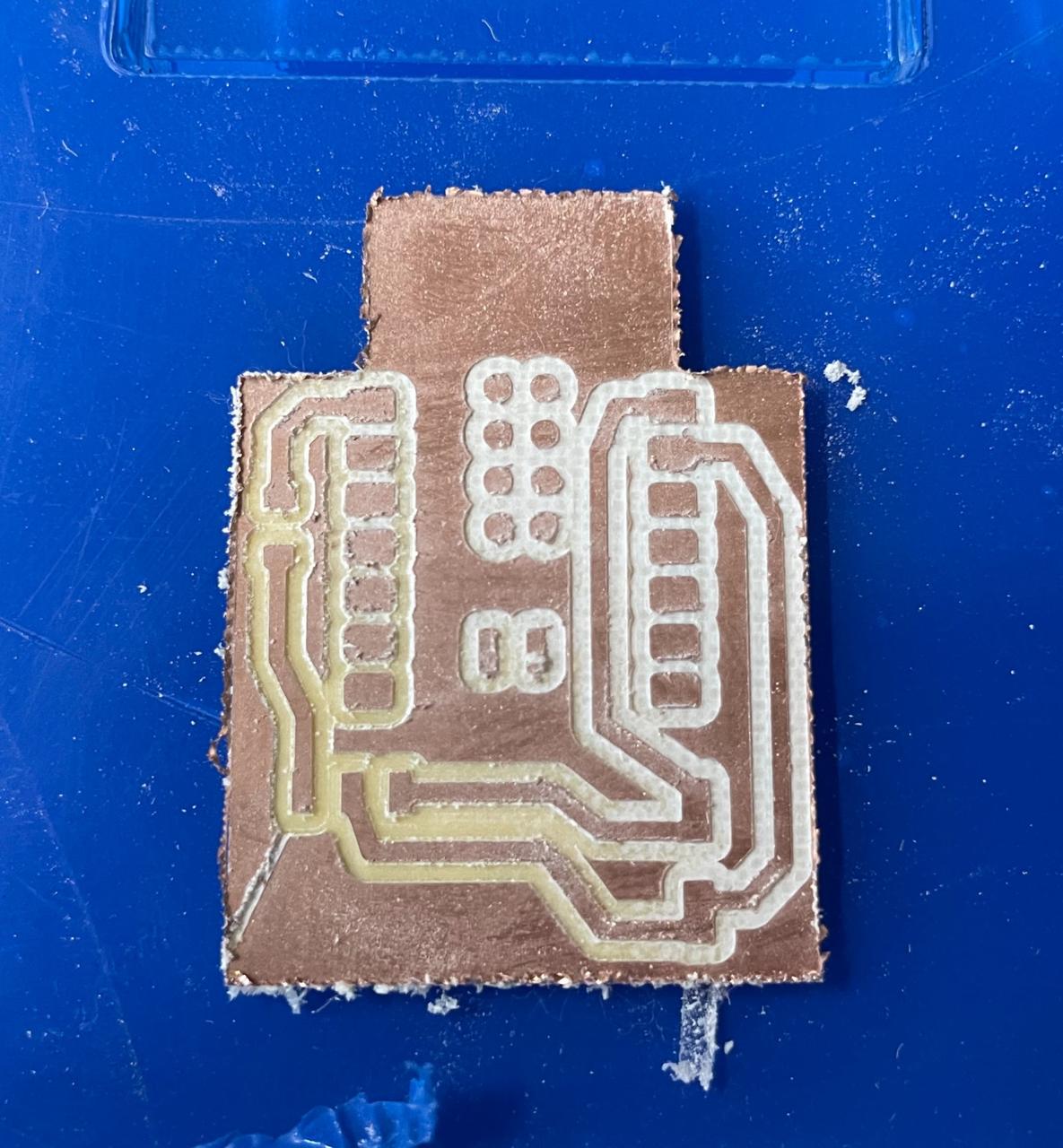
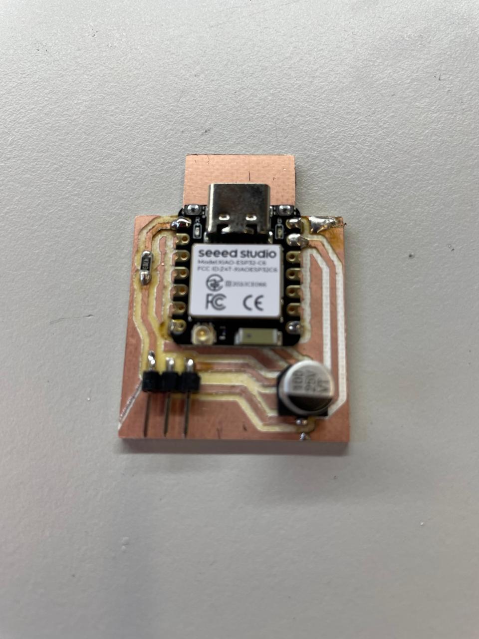
Once the milling was done, I removed the board and gave it a light sanding to clear off the residual copper dandruff (yes, it’s a thing). Before soldering, I placed a strip of electrician tape on the back of the ESP32C6 — just in case any of the pads on the bottom decided to flirt with the copper traces below.
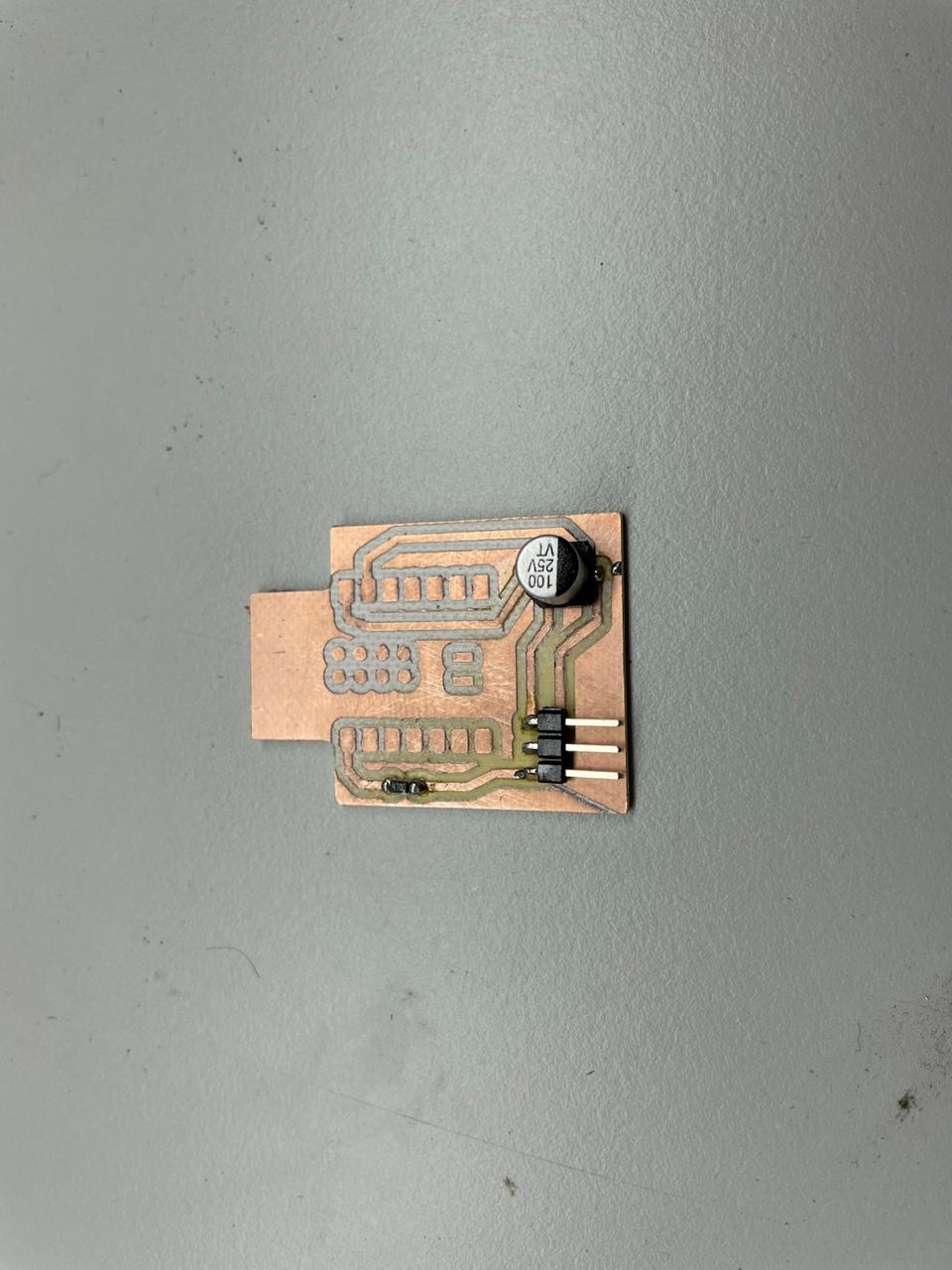
Then it was time to solder. I started with the tiny components: resistor, pin headers, and capacitor. Feeling confident, I moved on to the big boss: the XIAO ESP32C6. Not gonna lie, placing it correctly took me more than one try (and some whisper-yelling at the board).
Testing the Board
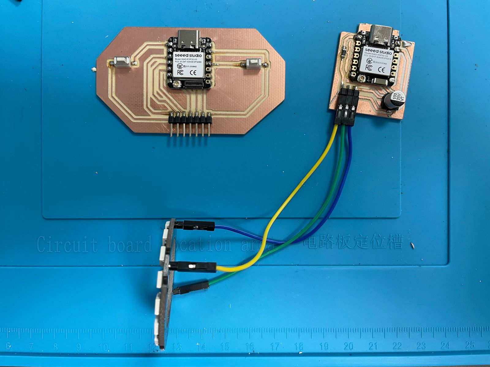
Once everything was soldered (and I convinced myself the pads hadn’t lifted), I connected it to the LED ring... and surprise: it worked! Just like the old deadbug version, except this one doesn’t look like I hot-glued a spider to a capacitor.
The board delivers power and data correctly to the ring, making it reusable for other sensors or modules too. A win!
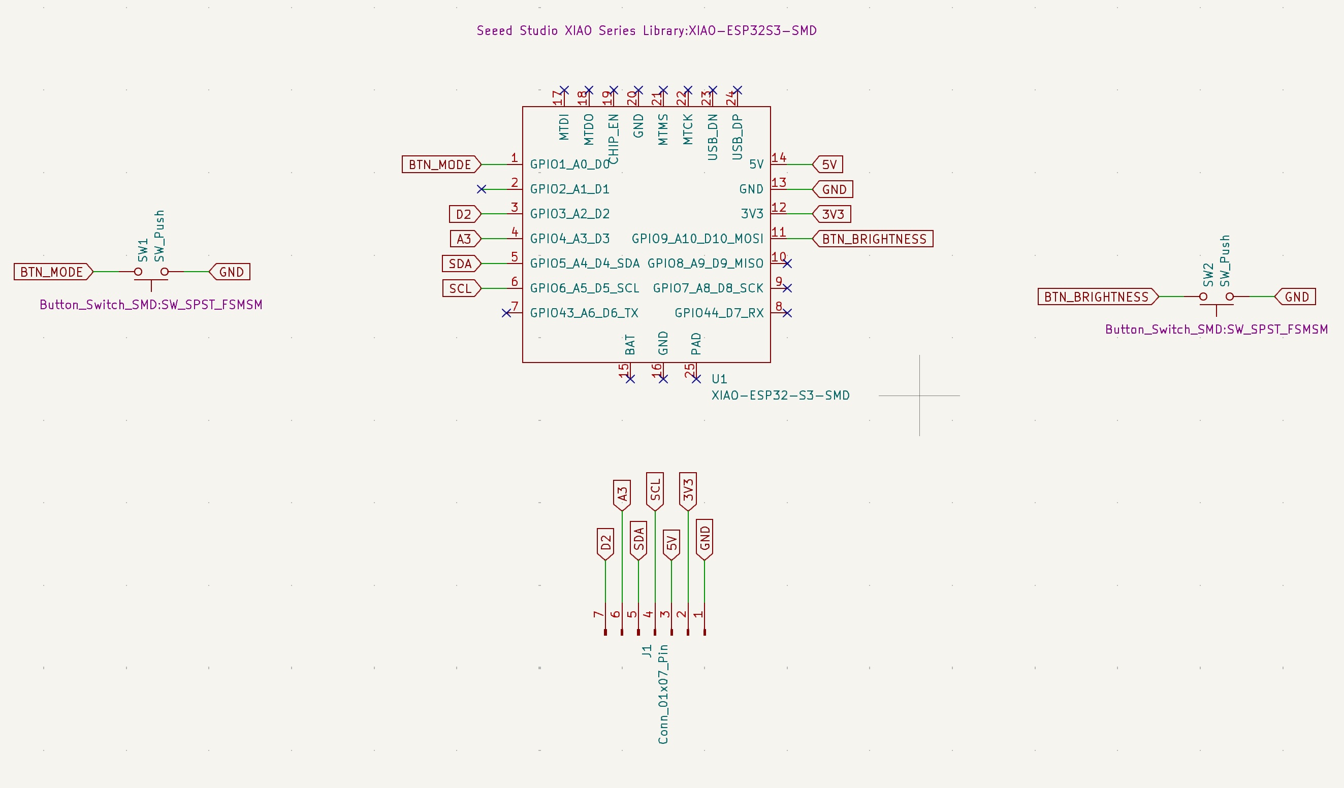
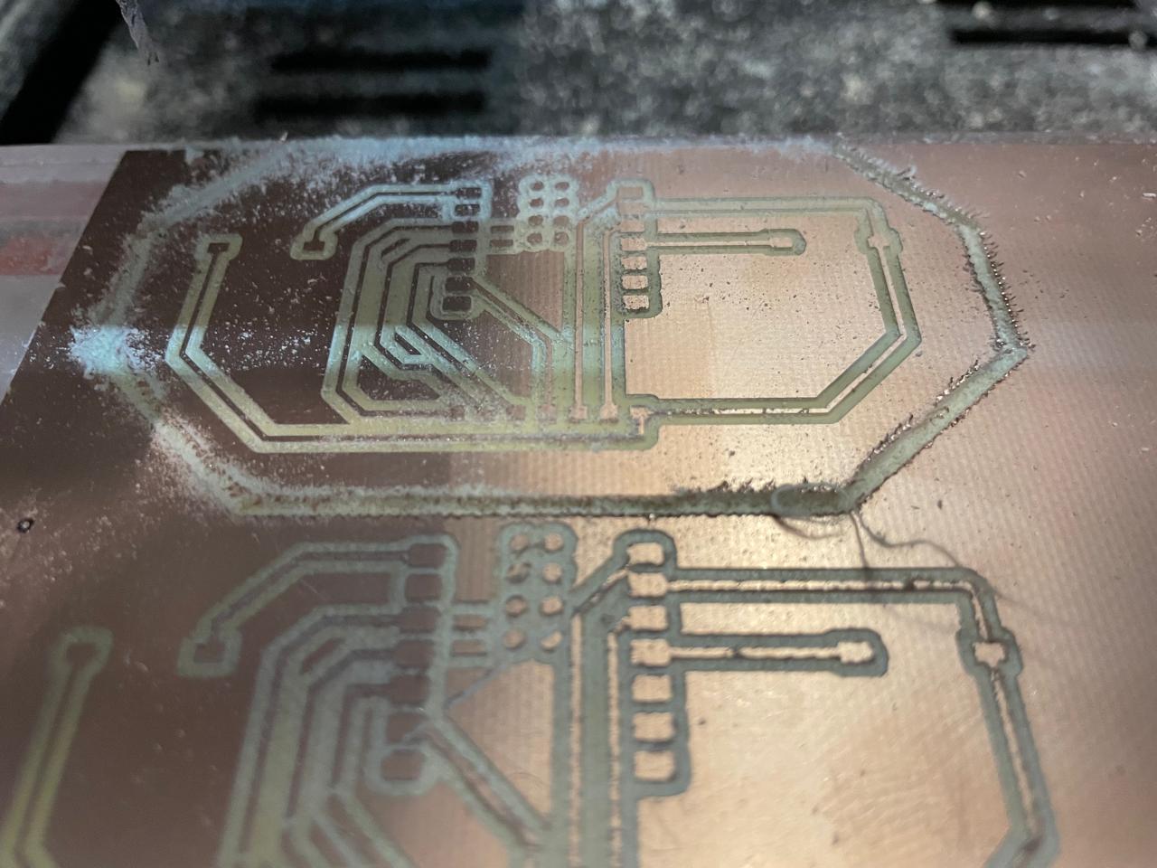
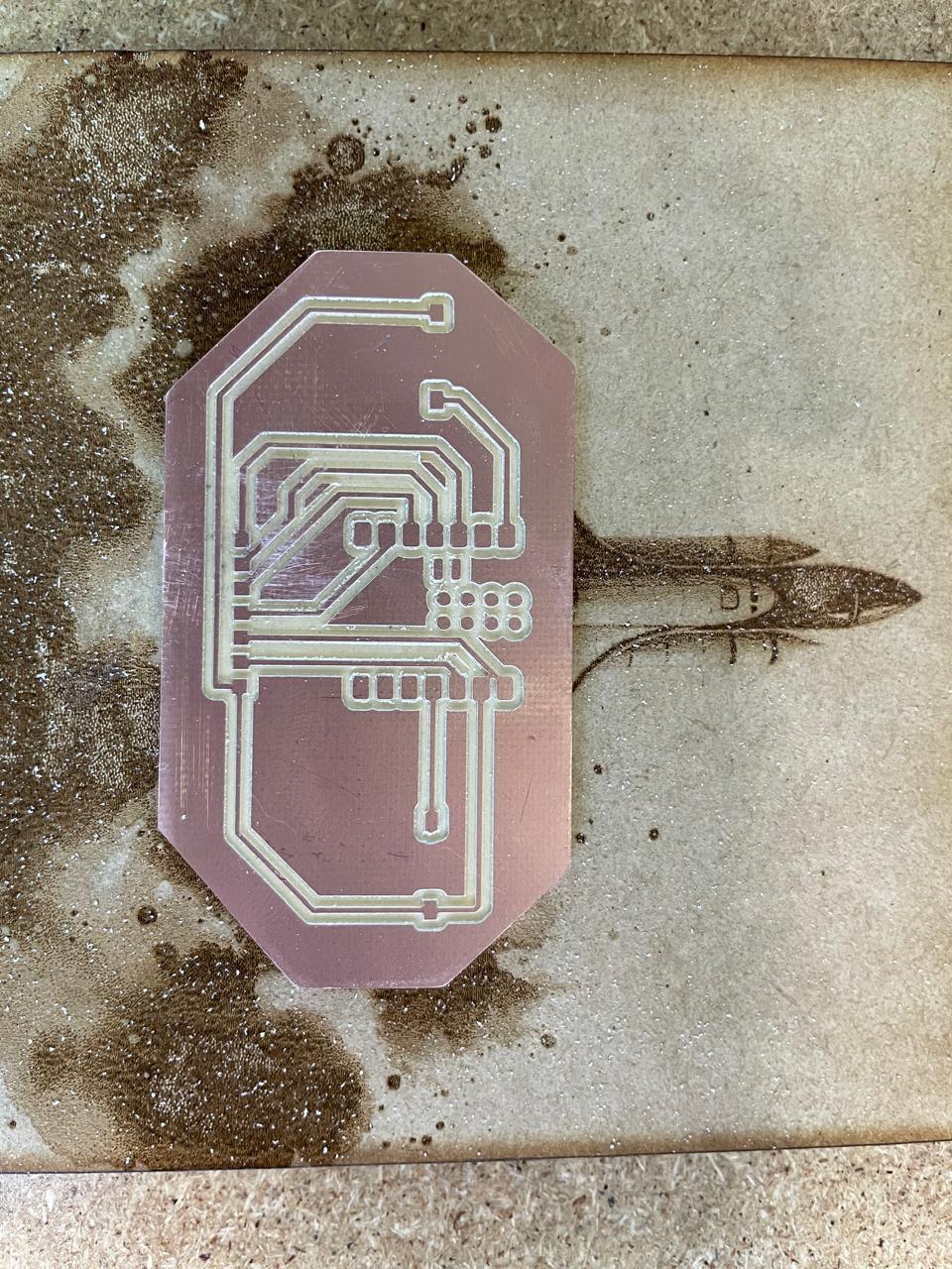
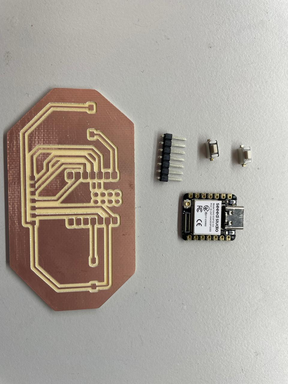
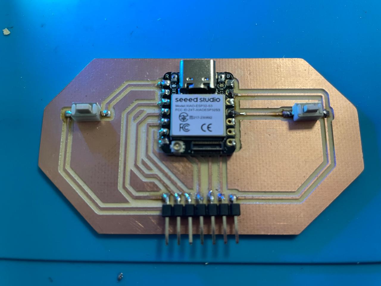
Bonus: Controller Board with ESP32S3 Sense
I designed a second PCB using an ESP32S3 Sense board. This version includes only two buttons and will be used as a standalone controller for other projects. The board’s role will be explained in more detail in Week 11: Networking and Communications.
For now, here are some images of the schematic, the prepared board for cutting, a short video of the process, and the final result.
Lessons Learned
-
470kΩ ≠ 470Ω: I soldered the wrong resistor — yes, three extra zeroes of resistance. The data line to the NeoPixel was essentially meditating in isolation.
Fix: Bridged the pads with a piece of solder wire to test, then replaced it with the correct 470Ω SMD resistor.
Lesson: Always verify component values before soldering. Multimeter > assumptions. -
MODS is not your friend... until it is: I forgot to invert the SVG when milling traces, so the machine happily carved a reverse circuit like it was making anti-electronics.
Fix: Realized the mistake after wasting a board. Next time, I checked the preview and confirmed the trace paths before exporting.
Lesson: The MODS interface is weird, but not psychic. Always verify direction and layout. -
Jog height matters: I set all origin coordinates (X, Y, Z) to 0. The result? The endmill almost engraved a love letter into my board face-down.
Fix: Adjusted jog height and Z-home to something more... respectful. Also learned to isolate Z adjustments during tool changes.
Lesson: Z = 0 is not universal. Respect vertical space or scratch your board like it owes you money. -
Pin labels are confusing: I used D0 in the code without realizing it mapped to GPIO2. The NeoPixel ring sat there, unbothered, because the signal never reached it.
Fix: Switched to using the actual GPIO number (`#define LED_PIN 2`), and the LEDs suddenly cared about my existence.
Lesson: Learn your board’s pin mapping — D-labels lie. -
Solder bridges are a valid debugging tool: In a moment of desperation (and no spare resistors), I created a data path with a melted solder blob.
Fix: It worked. Temporarily. Then I did the responsible thing and soldered a real resistor.
Lesson: Solder bridges are ugly heroes. Use them for quick tests — not for production.
Hero Shot
The final showdown: on the right, the NeoPixel-powered main board; on the left, the minimalistic two-button controller. One lights up. The other presses your buttons. Both survived my soldering skills.
Design Files
This board uses the same code as my original prototype — a simple web interface that lets you control the LED ring through WiFi. You can pick colors, switch effects, or just sit back and watch it glow. Functional? Yes. Overengineered? Also yes.
Check the code for both boards in Week 11: Networking and Communications.
In addition to the Arduino sketch, I’m also sharing the complete KiCad project files for both the main board and the controller. Everything from schematics to final PCB layout is in there — mistakes included, you're welcome.