Week 6: Electronics Design
Overview
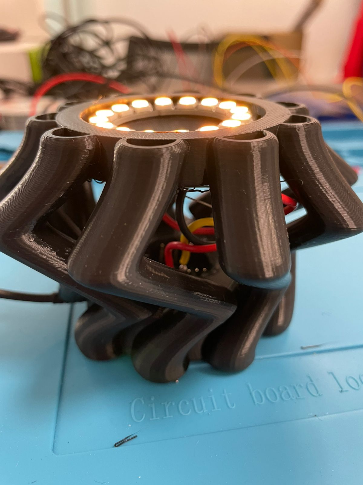
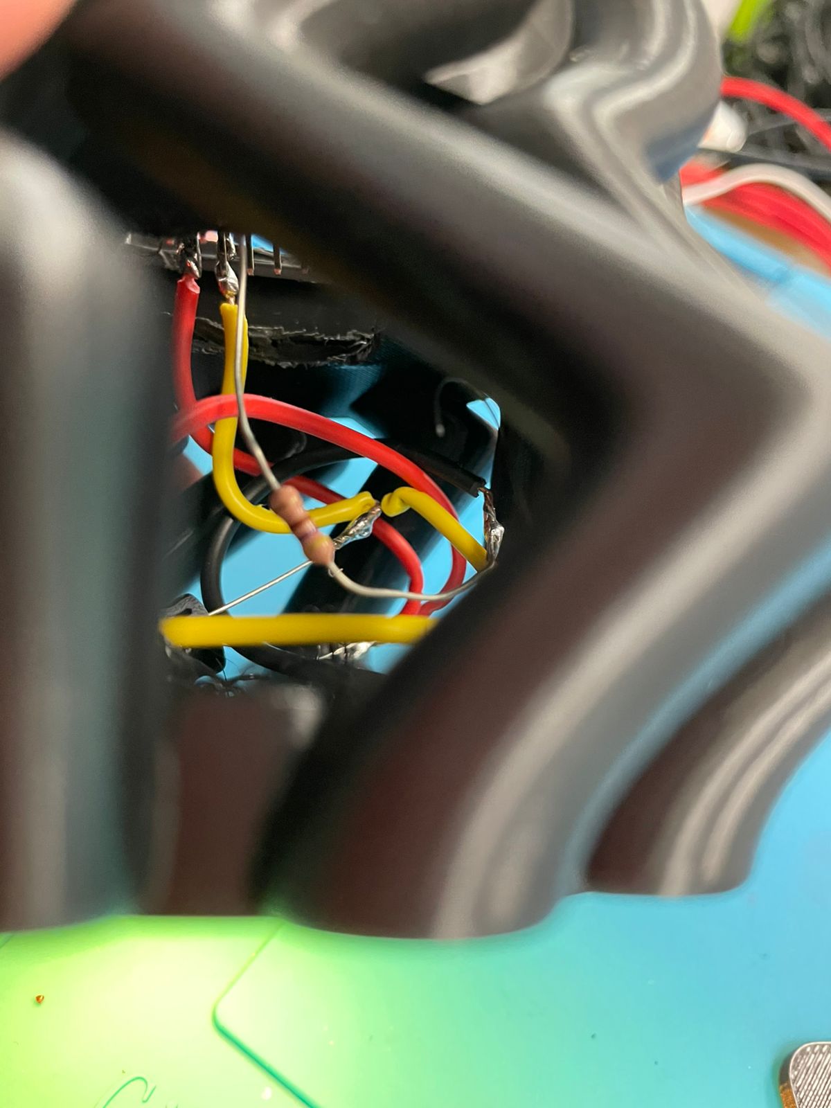
This week, I focused on designing a better circuit for my project, building on the work I did in Week 5. Last week, I created a dead bug circuit using an ESP32C6 and a Neopixel ring, which connected to a web server and allowed users to select different lighting effects. The circuit was integrated into my 3D-printed crystal rock holder, making it a functional and visually appealing piece.
Checklist
Group Assignment: Electronics Design
As part of the group assignment, we explored lab instruments and PCB design processes to better understand how circuits are tested and manufactured.
Lab Test Equipment
We used various lab instruments to analyze and validate PCB designs. These tools were crucial in ensuring that circuits functioned as expected.
| Instrument | Purpose | Relevance to the Assignment |
|---|---|---|
| Multimeter | Used to measure voltage, current, and resistance in a circuit. | Essential for checking continuity and ensuring proper electrical connections in PCB designs. |
| Oscilloscope | Helps visualize electrical signals over time. | Used in the group assignment to analyze signal integrity and troubleshoot PCB traces. |
| Power Supply | Provides a stable voltage source for testing circuits. | Ensured that the designed circuits received consistent power during testing. |
For more details, visit the group assignment page: Group Assignment - Week 6
Findings
Electronics design is not an easy assignment when you have little experience making circuits. However, having a solid grasp of the basics and using the right tools can make a big difference.
With the support of Puebla’s FabLab staff, I learned that even complex circuits become manageable when broken down into smaller tasks. Designing a PCB requires patience, but the results are rewarding when you see your custom board come to life.
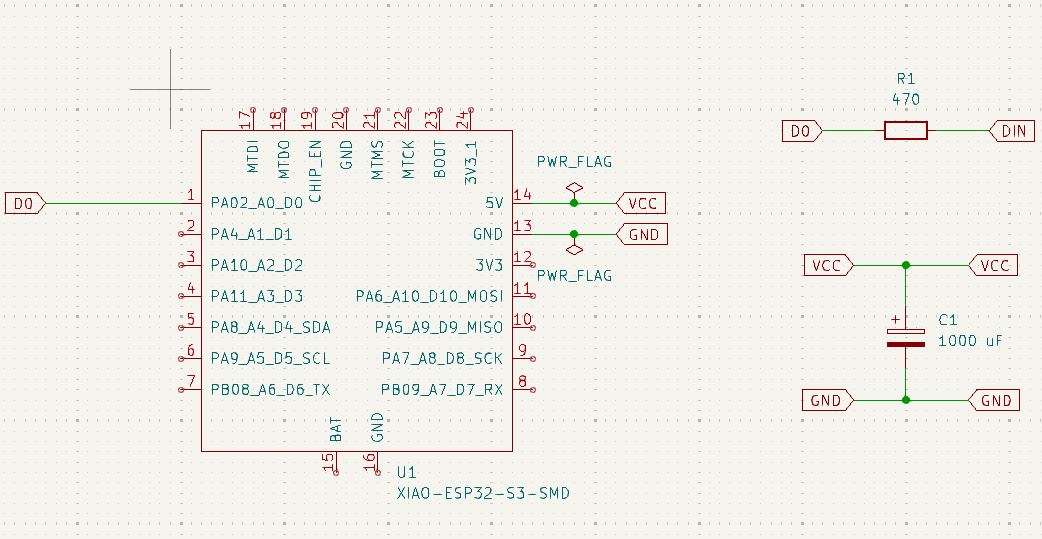
ESP32C6 (5V) + Neopixel Ring (WS2812B-16) Circuit Design
Understanding the Key Components
ESP32C6 Microcontroller (5V Version)
The ESP32C6 is a Wi-Fi and Bluetooth-enabled microcontroller. In this project, it controls the Neopixel Ring using a digital data signal.
- Operating Voltage: 5V
- GPIO Logic Level: 5V (matches Neopixel Ring requirements)
- Communication: Single-wire control via a dedicated GPIO pin.
Neopixel Ring (WS2812B - 16 LEDs)
The Neopixel Ring is a chain of 16 individually addressable LEDs that receive data signals from the ESP32C6.
- Operating Voltage: 5V
- Data Logic Level: 5V (fully compatible with ESP32C6 5V output).
- Pins:
- VCC: 5V power input.
- GND: Common ground.
- DIN: Data input (receives signal from ESP32C6).
- DOUT: Data output (used for daisy-chaining multiple Neopixel rings).
Circuit Explanation
I used CircuitLab to create this schematic. CircuitLab is an in-browser schematic capture and circuit simulation software tool to help you rapidly design and analyze analog and digital electronics systems
CircuitLab FAQThe following schematic shows the correct way to connect the ESP32C6 to the Neopixel Ring:
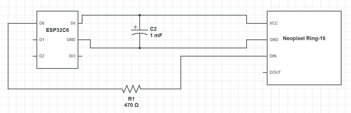
Power (5V & GND)
Since the ESP32C6 and the Neopixel Ring both run at 5V, they can share the same power supply.
- VCC (5V) from ESP32C6 → VCC on Neopixel Ring
- GND from ESP32C6 → GND on Neopixel Ring
Data Line (GPIO → Neopixel DIN)
The Neopixel Ring requires a single data signal to control the LEDs. The ESP32C6 sends this data through a dedicated GPIO pin.
- ESP32C6 GPIO (D0) → Data In (DIN) on Neopixel
- A 470Ω resistor is placed in series to reduce noise and voltage spikes.
Capacitor (C2: 1000µF)
A 1000µF capacitor is placed between 5V and GND to stabilize power.
- Purpose: Prevents voltage drops when multiple LEDs turn on at once.
- Placement: As close to the Neopixel Ring as possible.
Calculating the Resistor (R1)
The Neopixel Ring (WS2812B) is sensitive to voltage spikes, and a resistor helps prevent signal ringing.
Reference:
- Adafruit recommends a 330Ω - 470Ω series resistor to reduce noise and protect the first LED. [Adafruit Neopixel Überguide]
- The WS2812B datasheet suggests stable signal conditioning for reliable operation. [WS2812B Datasheet]
Calculating the Capacitor (C2)
When multiple LEDs turn on at full brightness, they draw high current. Without a capacitor, voltage fluctuations may cause flickering or unexpected resets.
Reference:
- Adafruit recommends a minimum of 1000µF for larger Neopixel installations. [Adafruit Neopixel Überguide]
Final Thoughts
The circuit follows best practices for Neopixel integration:
- ✅ ESP32C6 (5V) directly powers the Neopixel Ring (5V).
- ✅ 5V logic ensures stable data communication without a level shifter.
- ✅ A 470Ω resistor protects the data line.
- ✅ A 1000µF capacitor stabilizes power, preventing flickering.
Getting Started with KiCad
To design the PCB for this project, I used KiCad, an open-source electronic design automation (EDA) tool. The official documentation provides an excellent introduction:
- KiCad Getting Started Guide: [KiCad Documentation]
- KiCad Video Tutorial: [YouTube Tutorial]
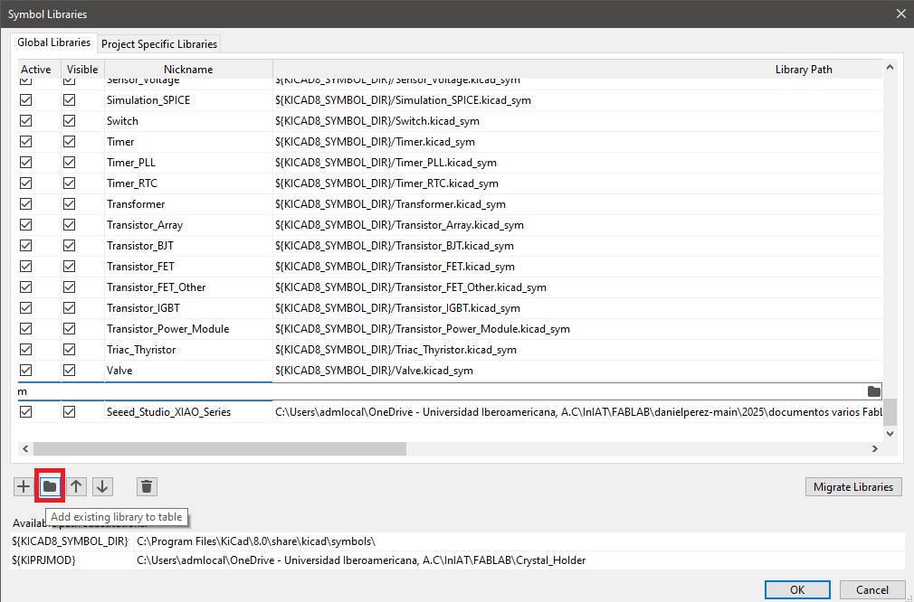
Step 1: Adding the Xiao ESP32C6 Library
The Xiao ESP32C6 was not included in the default KiCad library, so I had to download it separately. The official Seeed Studio KiCad library is available on GitHub, and I followed the provided instructions:
To easily download the library, I cloned the GitHub repository using the following command:
git clone https://github.com/Seeed-Studio/OPL_Kicad_Library.git
It is important to download the library to a proper directory where it can be easily accessed for the next step.
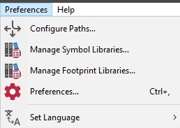
Step 2: Adding the Library to KiCad
Once the library was downloaded, I added it to KiCad:
- Go to Preferences > Manage Symbol Libraries and select the downloaded library.
- Repeat the process for footprints by going to Preferences > Manage Footprint Libraries.
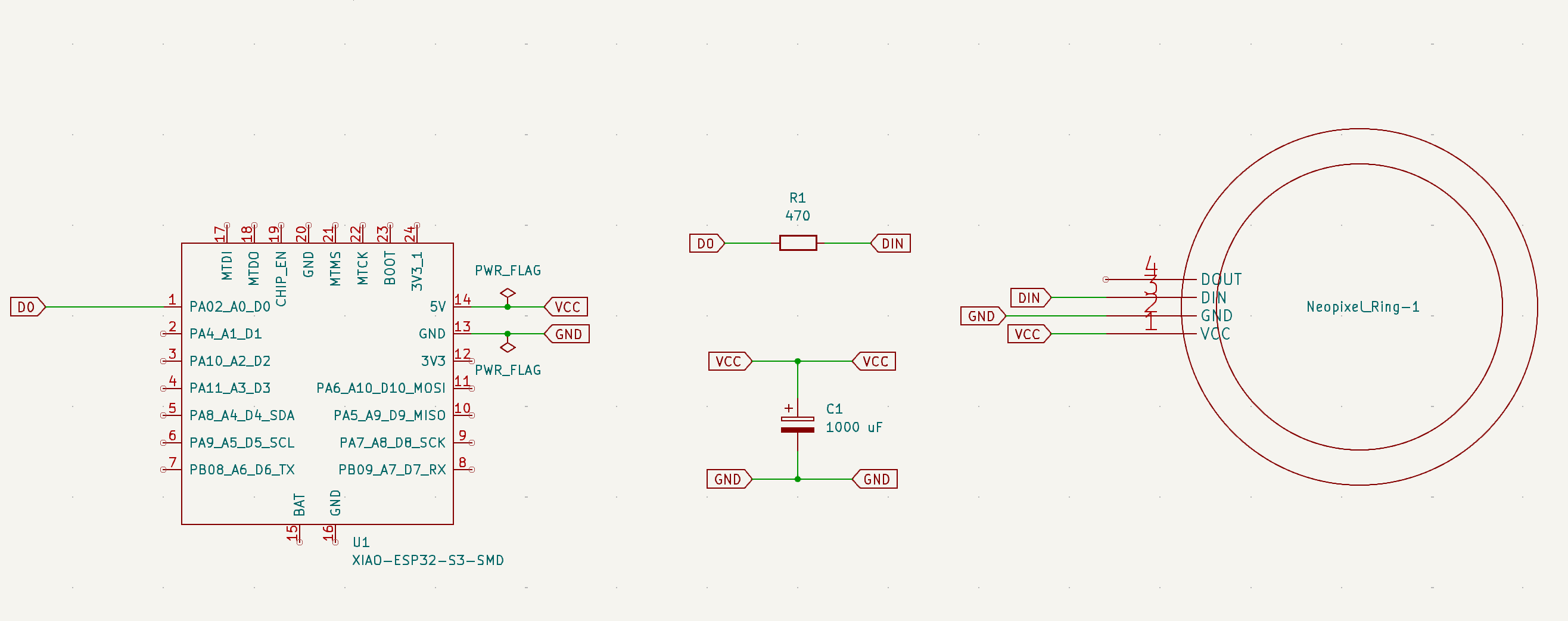
Step 3: Creating the Schematic
After successfully adding the ESP32C6 library, I started designing the schematic.
Step 4: Creating a Custom Symbol and Footprint for the Neopixel Ring
Since I could not find a predefined symbol or footprint for the Neopixel Ring, I had to create my own. While not difficult, the process required attention to detail.
Creating the SymbolUsing the Symbol Editor, I defined a new component with the correct pin configuration for the Neopixel Ring. This involved:
- Defining the pin names: VCC, GND, DIN, and DOUT.
- Ensuring the symbol was properly classified and saved.
Next, I used the Footprint Editor to create a matching physical layout:
- Positioning the pads to match the Neopixel Ring’s physical connections.
- Defining the footprint shape to reflect the real component.
- Saving the footprint to my custom library.
Step 5: Completing the Schematic
With all necessary symbols and footprints in place, I completed the schematic, ensuring that all connections matched my original design.
Step 6: Designing the PCB
After finishing the schematic, I moved to the PCB Editor to arrange components and route the traces.
- Placed components according to the schematic.
- Used the routing tool to connect traces.
- Optimized the layout for manufacturing.
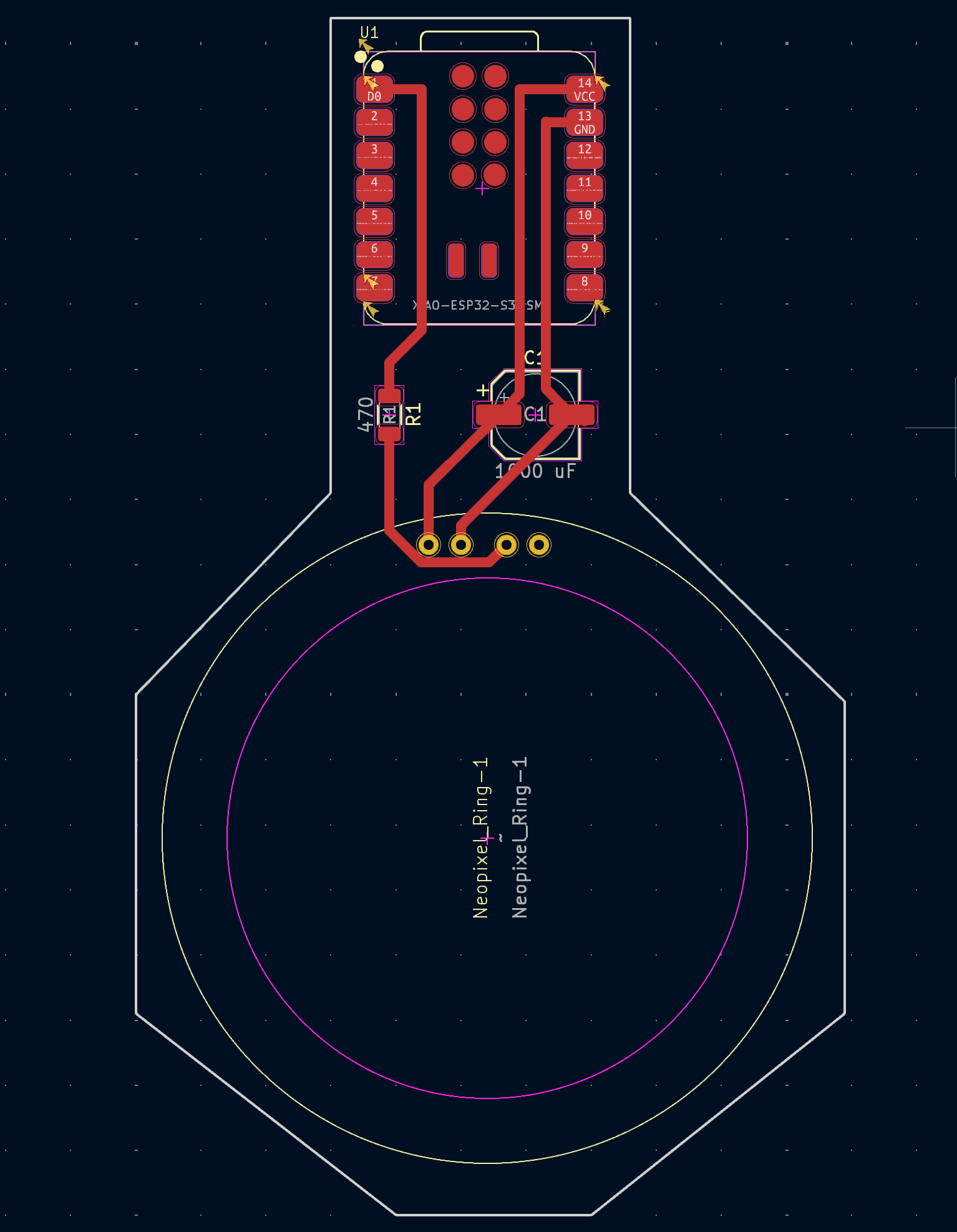
Step 7: 3D Rendering and PCB Production
KiCad provides a powerful 3D viewer that allows previewing the PCB before production. This helped in verifying component placement and overall design accuracy.
In the upcoming weeks, I will fabricate a PCB using two methods:
- Milling the PCB in the FabLab.
- Ordering the PCB from a manufacturer.
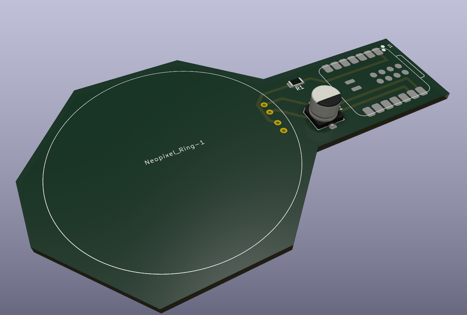
KiCad's features made the design process intuitive and efficient, allowing for a streamlined workflow from schematic creation to PCB layout and rendering.
Download Project Files
All project files, including the schematic, custom footprint and symbol for the Neopixel Ring, and Gerber files for PCB manufacturing, are available in the following archive:
These files include:
- The complete KiCad project files.
- The custom footprint and symbol for the Neopixel Ring.
- The exported Gerber files for PCB manufacturing.
These files can be used to reproduce the PCB design, modify the schematic, or send the board for fabrication.