Electronics Design
Linked to the group assigment page
About PCB
One of the most prominent aspects of printed circuit boards (PCBs) is their function as electrical connectors between electronic components through traces and pads. These boards, constructed with layers of various laminated materials, facilitate the routing of signals and power between physical devices. Soldering acts as both an electrical conductor and a strong mechanical adhesive. Additionally, there are various materials for PCBs, each with its specific characteristics. For example, FR4, the most commonly used, employs fiberglass as a base. It is essential to understand key terms related to PCBs, such as "annular ring," "design rule check (DRC)," and "solder mask," among others, to comprehend their design and fabrication.
PCB Design and Fabrication Process
Electronic PCB Design with KiCad:
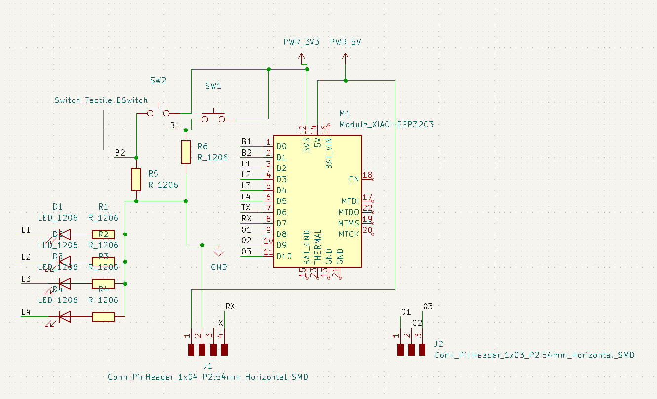
- Schematic Creation: Using KiCad, the circuit schematic is created by placing components and connecting them correctly.
- Pros: Intuitive interface, extensive component libraries.
- Cons: Initial learning curve.
- Footprint Assignment: Instructors of Fab Lab Puebla provided a file with footprints of materials available in the lab, easing footprint assignment in KiCad.
- Pros: Access to specific footprints available in the lab, simplifies footprint assignment.
- Cons: Depends on the availability and variety of provided footprints.
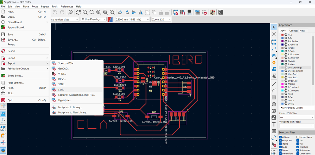
- Exporting Design as SVG: The design is exported as an SVG file from KiCad to be later imported into MODS.
- Pros: Facilitates parameter configuration in MODS.
- Cons: May require manual adjustments to ensure accuracy in conversion.
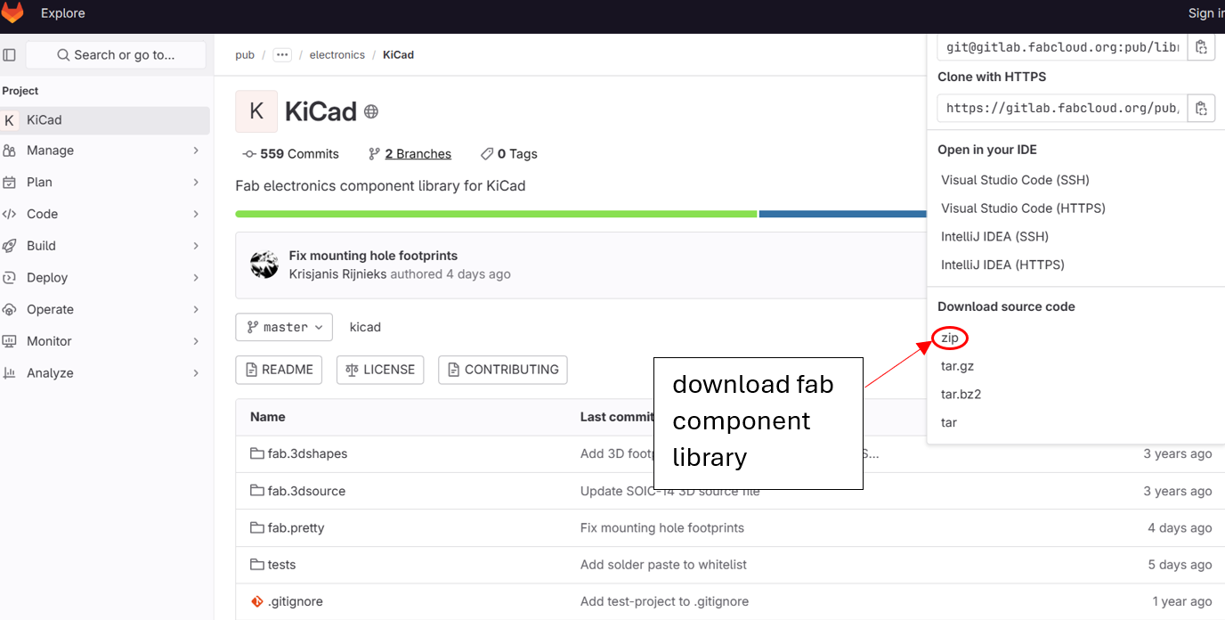
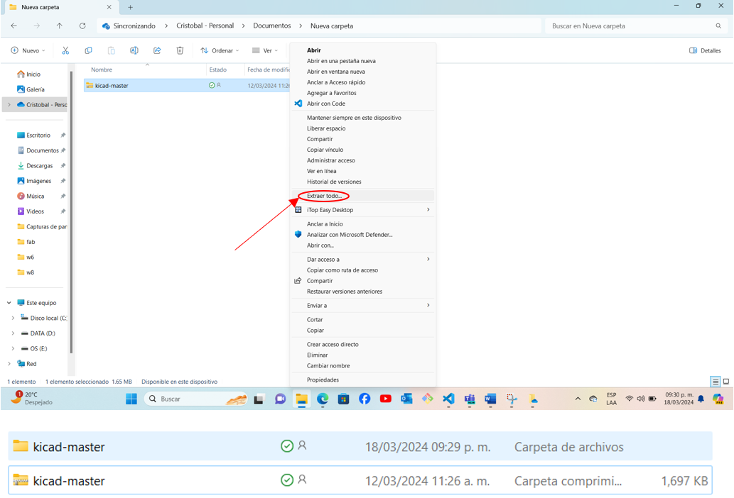
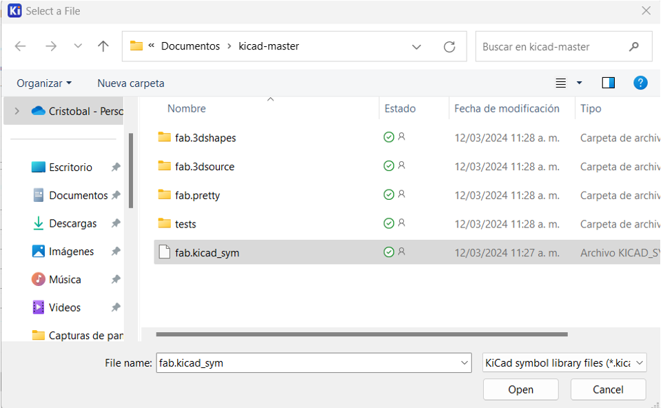
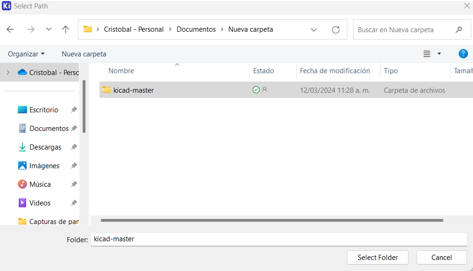
Download and unzip fab components library
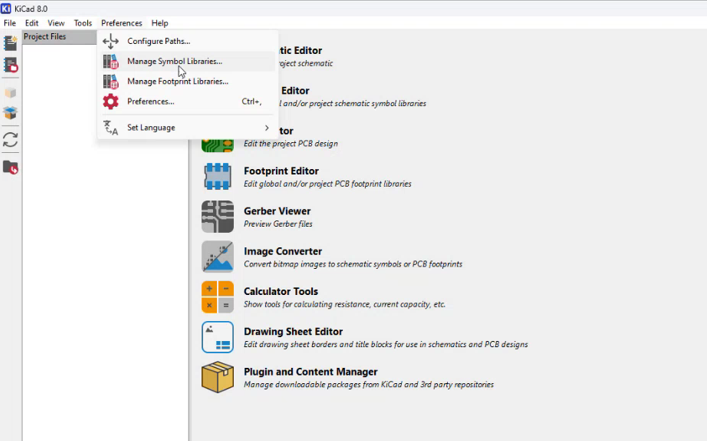
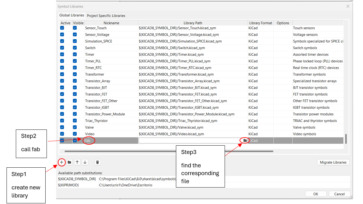
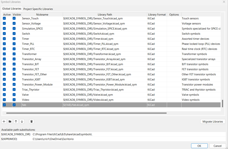
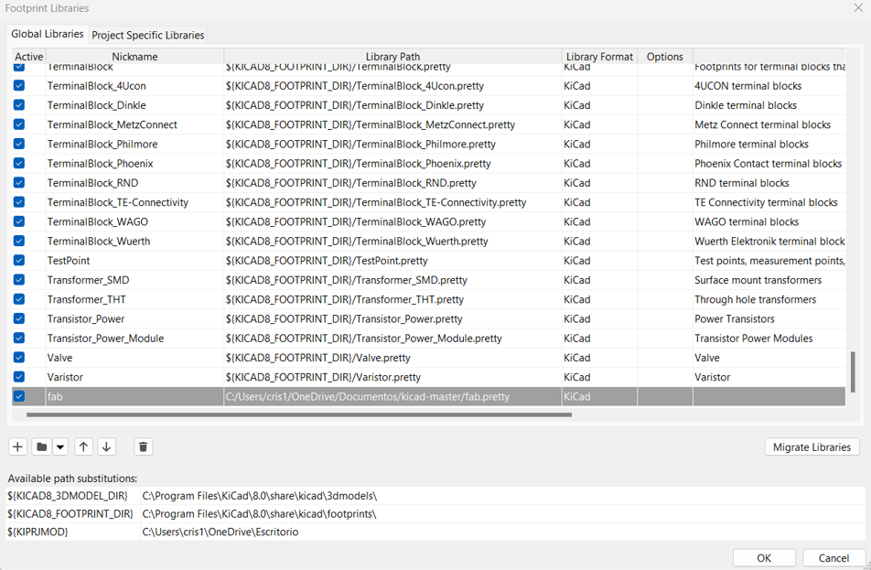
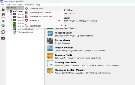
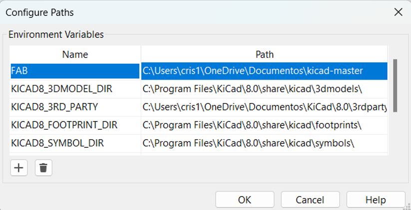
Kicad folders configuration
Symbol libraries
Footprint libraries
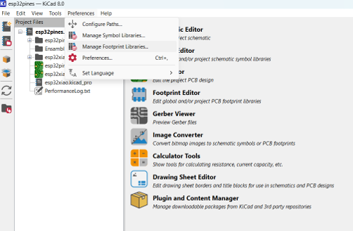
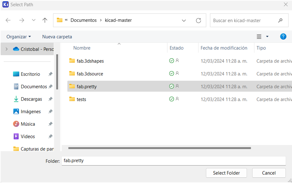
Configure paths
New project
Schematic editor
Main Commands:
- Create components: Use the "Add Component" tool to select and place components on the schematic.
- Connect components: Use the "Connect Wires" tool to connect the pins of components according to the circuit design.
- Edit component properties: Double-click on a component to edit its properties, such as value, reference, etc.
- Add labels and names: Use the "Label" tool to add names and labels to components and connections.(control + l)
- Anchor connection points: Connection points are implicit in the components, but you can adjust them if necessary to facilitate the connection.
- Delete components and connections: Use the "Delete" tool to remove unwanted components or connections.
- Rotate and move components: Use the "Move" tool to move components and the "Rotate" tool to rotate them as needed. (control + R)
- Adjust zoom and view: Use the zoom and navigation options in the toolbar to adjust your view.
- Save and load projects: Use the save and load options in the File menu to save and open projects.
- Generate Bill of Materials (BOM): KiCad can automatically generate a bill of materials based on the schematic. This option is available in the project output generation.
PCB editor
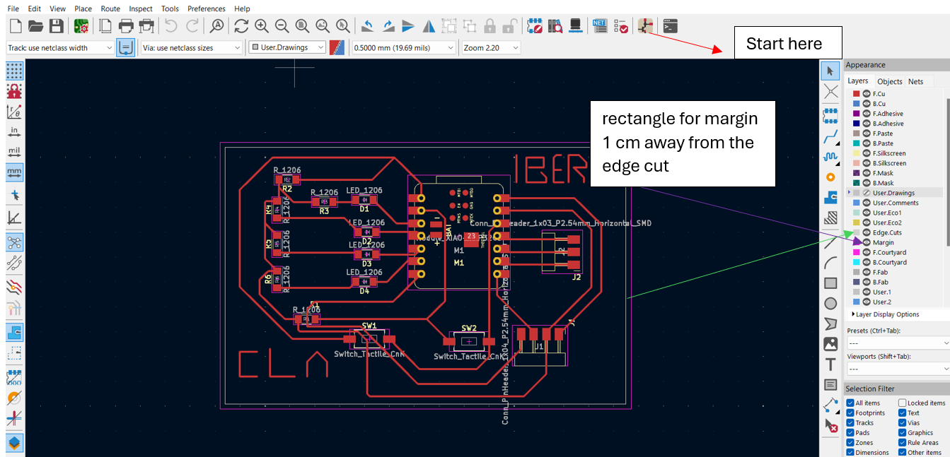
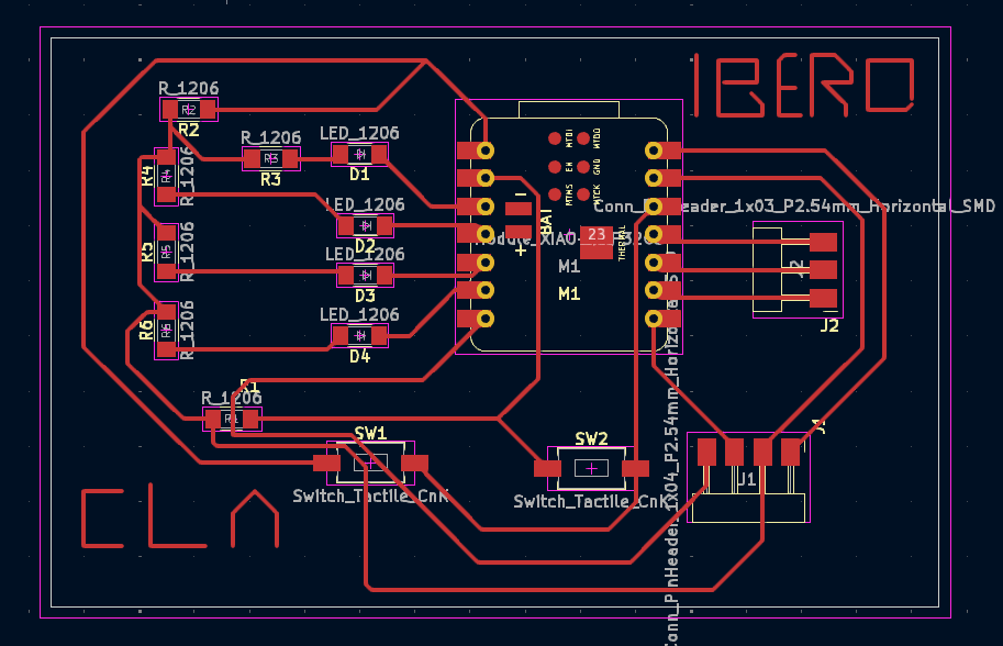
With the selected tool in F.Cu, if you press the 'x' key, you can draw the tracks.It's easy since the program tells you what to join with what, with what if something laborious when the tracks start to join together too much and there is no longer a step, it's like a game if that's how you want to see it.
When you finish joining, a rectangle is made with the edge cut tool, I mark this tool with a green arrow and the gray rectangle, this rectangle is responsible for mentioning which part will be cut.
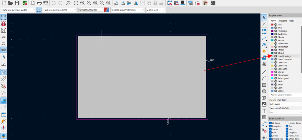
It is also important to make another rectangle with the margin tool, which I show with a purple arrow and the rectangle is pink, and this is responsible for indicating an area around the edge of the PCB that must be kept free of components and traces. This margin ensures that there are no components or traces too close to the edge of the PCB, which could cause problems during the manufacturing or assembly process.
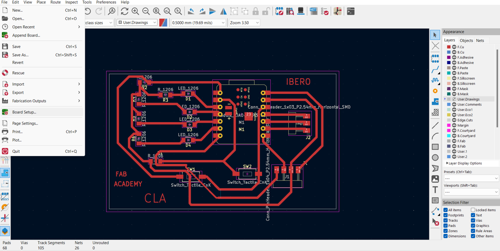
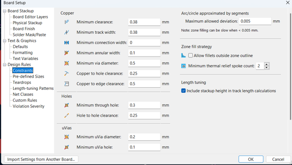
1. open board set up
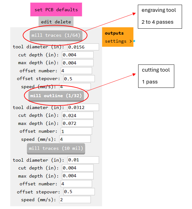
in this step first open board set up and then click contrains, I set up the design rules (DRC) to ensure that the PCB works well and can be manufactured without issues. I specified values like 0.38 mm for the minimum trace clearance and width to help prevent overheating and avoid short circuits. I also set the minimum via diameter to 0.5 mm to ensure that the holes are large enough to reliably connect different layers of the PCB. Additionally, I configured a minimum copper-to-hole clearance of 0.25 mm to prevent drilling problems and a 0.5 mm clearance from the copper to the edge of the PCB to avoid damage during cutting. These settings are important for the ESP32-WROOM module to function properly and for the PCB to be manufactured correctly.
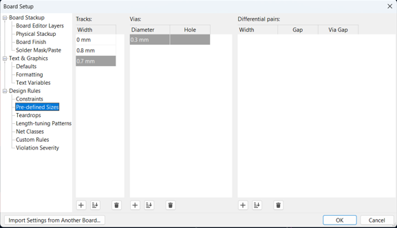
In this step, set the width of the track to 0.7 mm so that the machine does not have a hard time doing it and has problems like breaking a track or something like that.
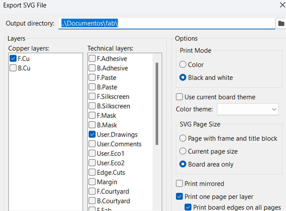
Export in format svg and black and white
During this week, we will be creating a PCB. It's simply a matter of putting theory into practice, programming the machine regarding speeds, axes, among other settings, as will be demonstrated in the following visual aids. It's worth mentioning that a ROLAND SRM-20 machine will be used for this purpose.
ROLAN SRM-20 steps
- Setting Up in MODS: The SVG file is imported into MODS, where all necessary parameters for manufacturing on the SRM-20 are configured.
- Pros: Allows precise configuration of manufacturing parameters.
- Cons: Requires knowledge of SRM-20 specifications and materials used.
- Generation of .RML Files: MODS generates two .RML files, one for cutting and another for track engraving, based on the established configuration.
- Pros: Automates the generation of specific files for the SRM-20.
- Cons: Requires precise configuration in MODS to ensure quality of the final result.
For making the files compatiblle for the machine (.rml) we will use the software called Mods.
In this first video, we can see the steps for setting up the program for PCB engraving.
For cutting, it's the same process, except that for the PNG, we will add the invert button and we changed de tool.
Manufacturing on a Roland SRM-20:
Steps for the machine
Safety bed
In this step, we will use knowledge previously seen in week 3 to cut our safety bed on the laser CNC.
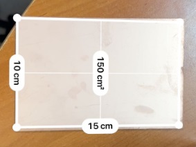
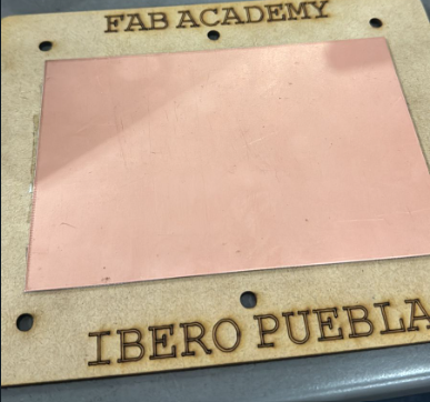
Then, we measure and adhere a copper plate.
Program and Driver
To use the machine, we need to install a program and a driver.

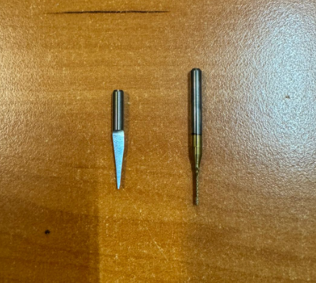
Identify tools
We are going to use a 15 degree V-bit for engraving and a 0.8 mm end Mill for cutting.
The tool on the left side is the engraver and the tool on the right side is the cutter that we will be using.
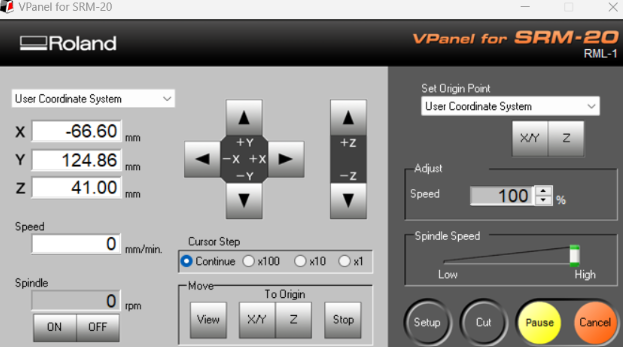
Sofware SRM-20
You have the option to manipulate the axis movement simply by clicking on the directional arrows. Additionally, you can designate the X/Y and Z origins from the options situated at the top right corner of the screen. It's also possible to toggle the spindle on or off as needed. Furthermore, you can navigate precisely to the origin point located at the bottom center of the screen. Adjustments to the approach speed can be made in the center of the screen When it comes to loading files and commencing cutting or engraving tasks, you'll find the necessary tools within the "Cut" section. Here, you can upload the engraving file to finalize the process, and if required, delete any previous engraving before adding the cutting file.
Calibrate, Engraving and Cut
First, secure the MDF with copper on the machine. Then, open the software and connect it to the Roland. Place the engraving tool and calibrate the X/Y axis around one centimeter from the bottom left corner. Next, lower the Z-axis near the board, adjusting the focus speed if necessary. Loosen the tool and allow it to touch the board before tightening it again. Save the X/Y/Z coordinates and move the tool upwards for safety. Finally, initiate the engraving process.
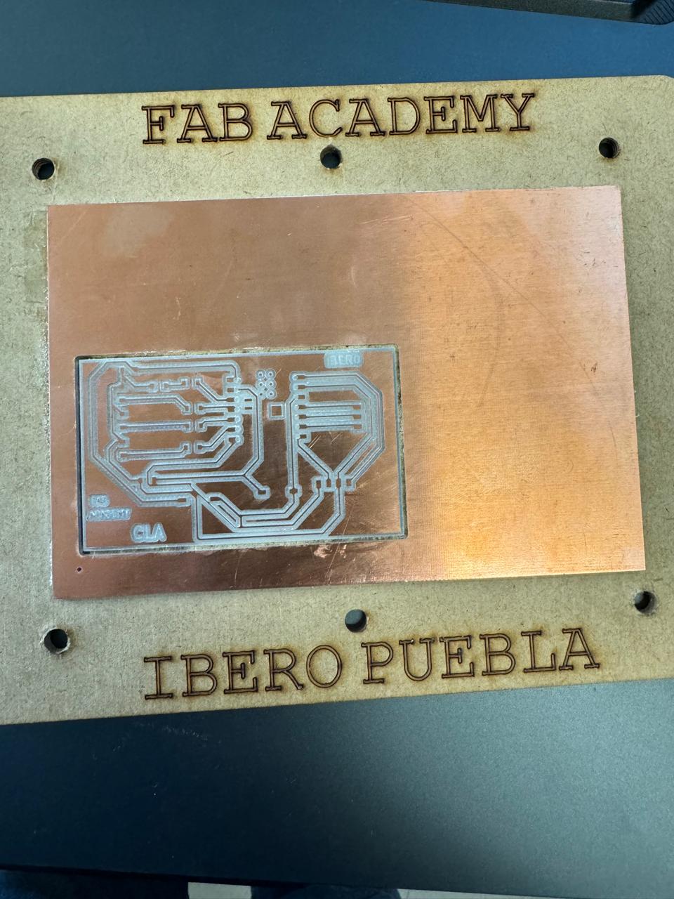
Once the process is complete, we proceed to vacuum up the remaining debris.
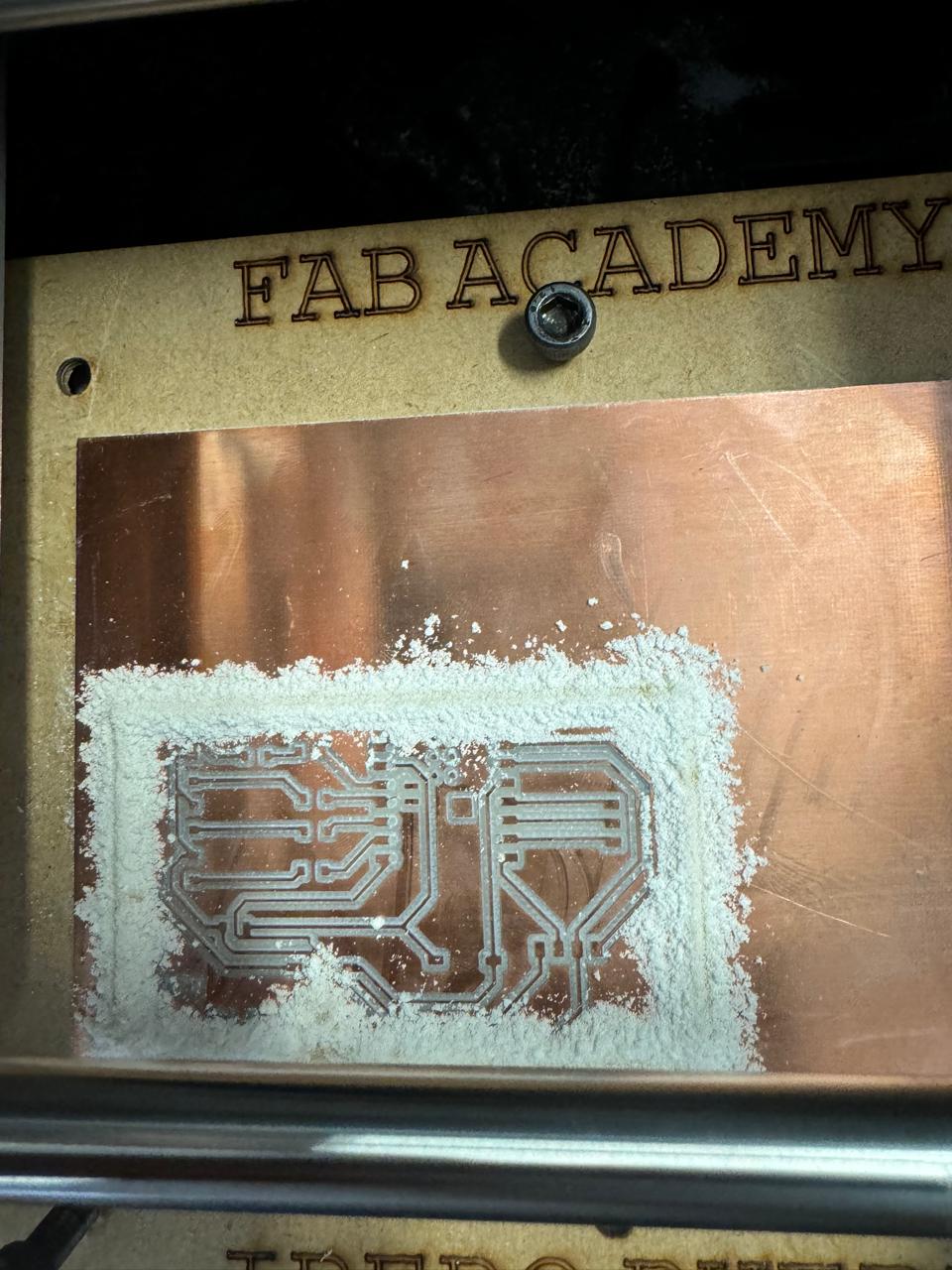
We change the tool to the cutting one and repeat the previous steps. The PCB should look like the one in the image.
Components and soldering
Tips for soldering like a pro
- Essential Tools: Use a quality soldering iron with a clean and fine tip for efficient heat transfer. You'll also need solder flux, quality solder, and anti-static tweezers for handling components.
- Temperature Control: Adjust the soldering iron temperature according to the type of component and the size of the copper traces on the PCB. Too high a temperature can damage components, while too low a temperature can result in weak joints.
- Proper Preparation: Clean the copper traces and pads with isopropyl alcohol and a soft brush before soldering to remove any residue. This ensures better solder adhesion.
- Use of Solder Flux: Apply a small amount of solder flux to the areas to be soldered to improve solder flow and adhesion. This helps prevent solder bridges and ensures solid connections.
- Soldering Technique: Keep the soldering iron in contact with the pad and component for a few seconds to allow heat to distribute evenly. Then, apply solder to the point of contact until the solder completely covers the pad and component.
- Avoiding Overheating: Avoid heating components for too long to prevent damage. Additionally, avoid applying too much solder, as it can cause short circuits between nearby traces.
- Inspection and Cleaning: After soldering, visually inspect all connections to ensure they are clean and shiny. Clean any excess solder or residue with isopropyl alcohol and a soft brush.
- Practice and Patience: Soldering on PCBs requires practice to master. Start with simple projects and practice regularly to improve your soldering skills. Be patient and don't be discouraged by initial mistakes, as practice will help you improve over time.
We proceed to solder.
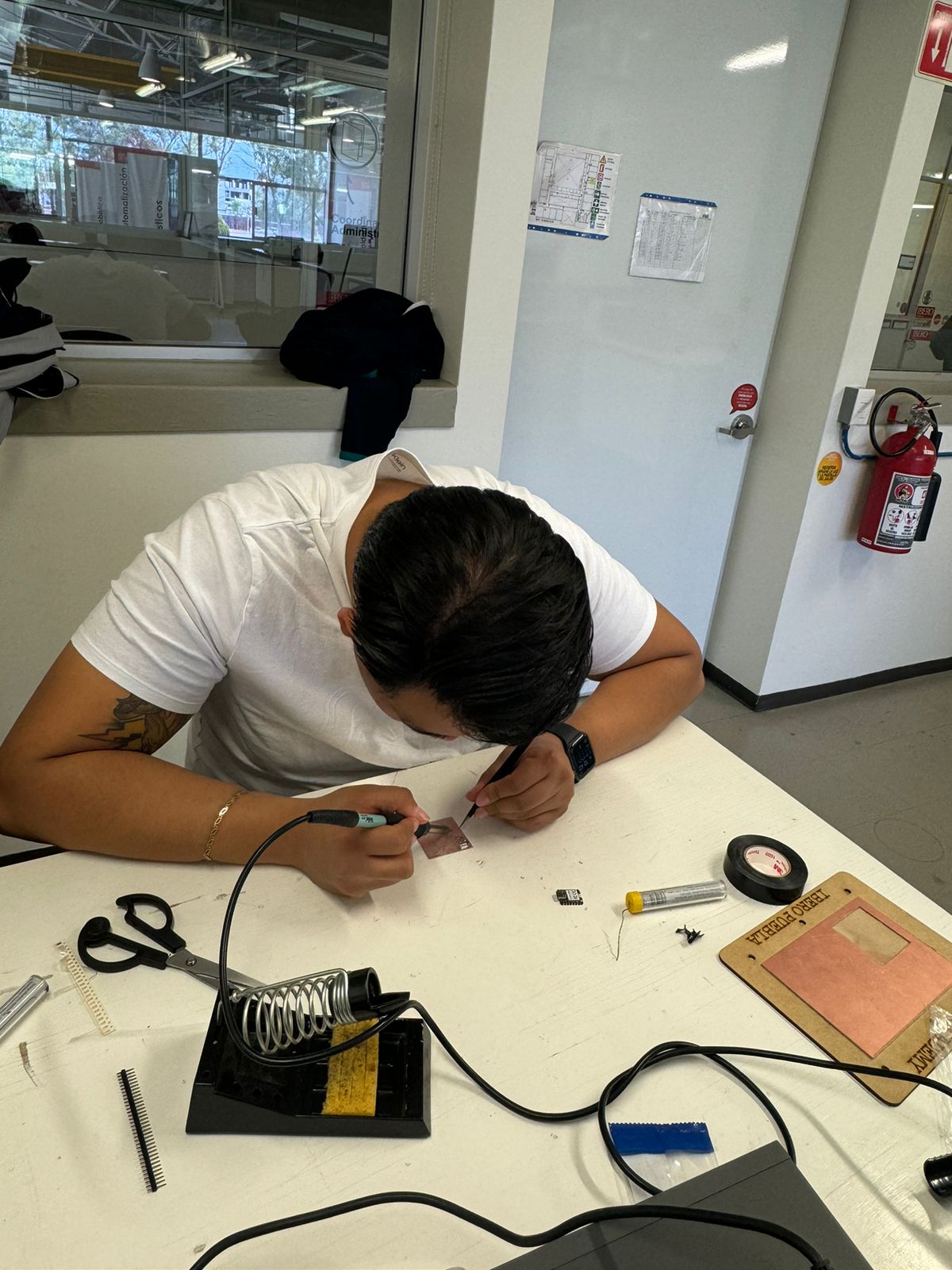
So that it finally looks like this.
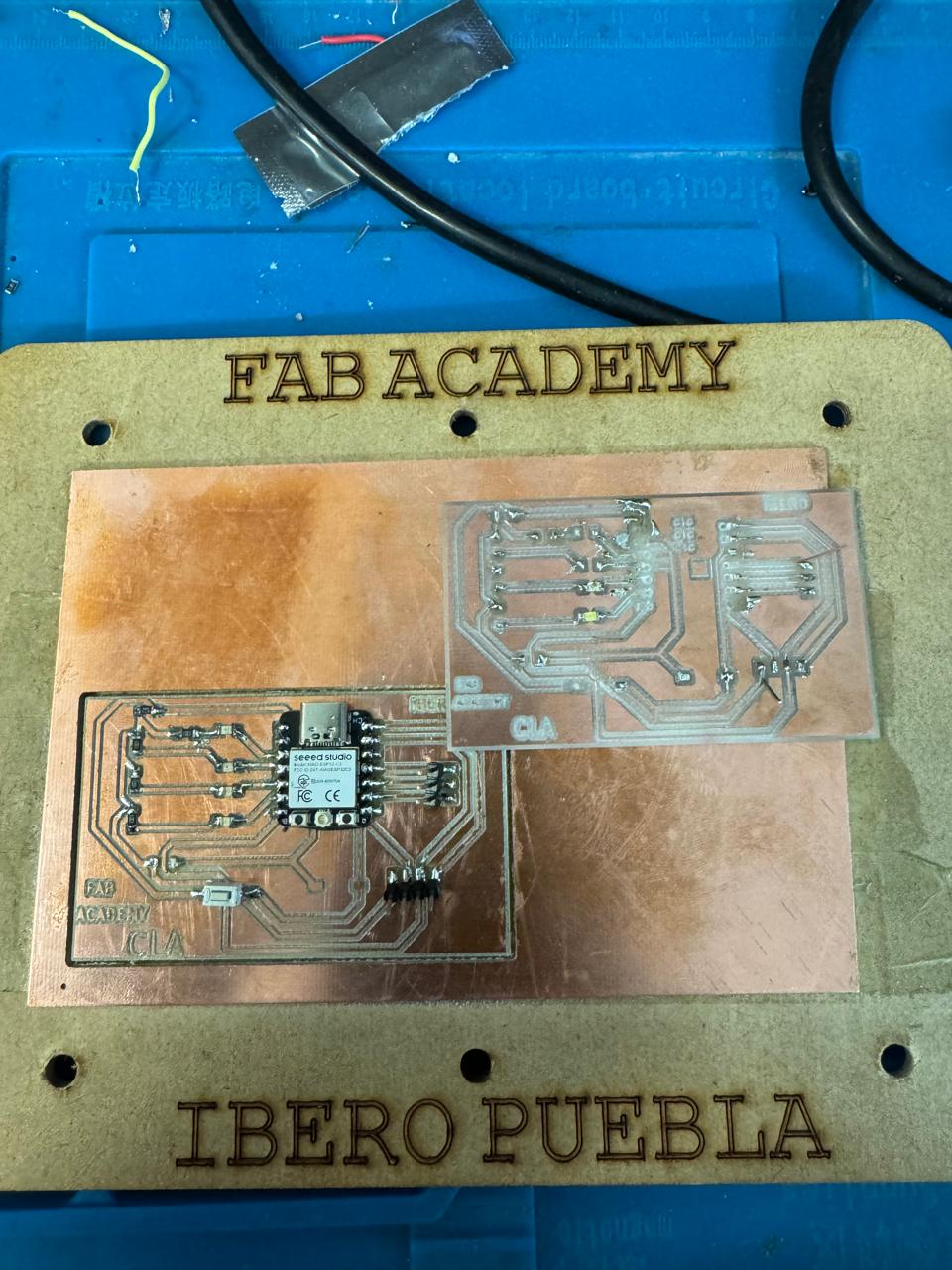
In the last photo we can see 2 pcbs since in the first pcb I made I didn't realize that the machine had not cut a track correctly, and because I was confident and didn't verify them either by sight or with a multimeter, it made a short in the xiao , affecting the operation
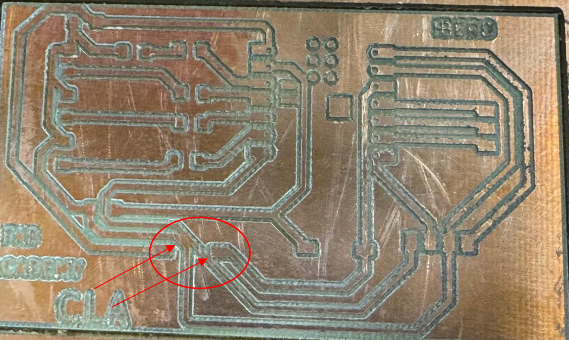
He proceeded to make the PCB once the error was detected, and this time it worked wonderfully.
Components:
| Qty | Description | Image |
|---|---|---|
| 1 | XIAO ESP32C3 | 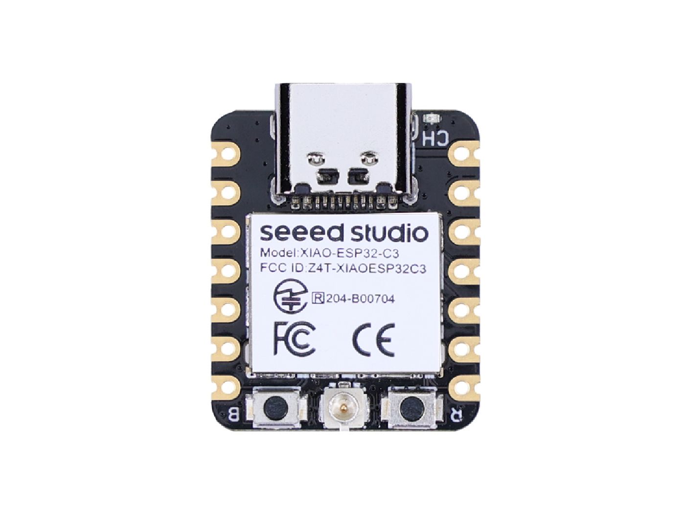 |
| 4 | 820 ohms resistor |  |
| 2 | 2.4 kΩ (242) resistor | 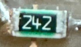 |
| 4 | Leds | 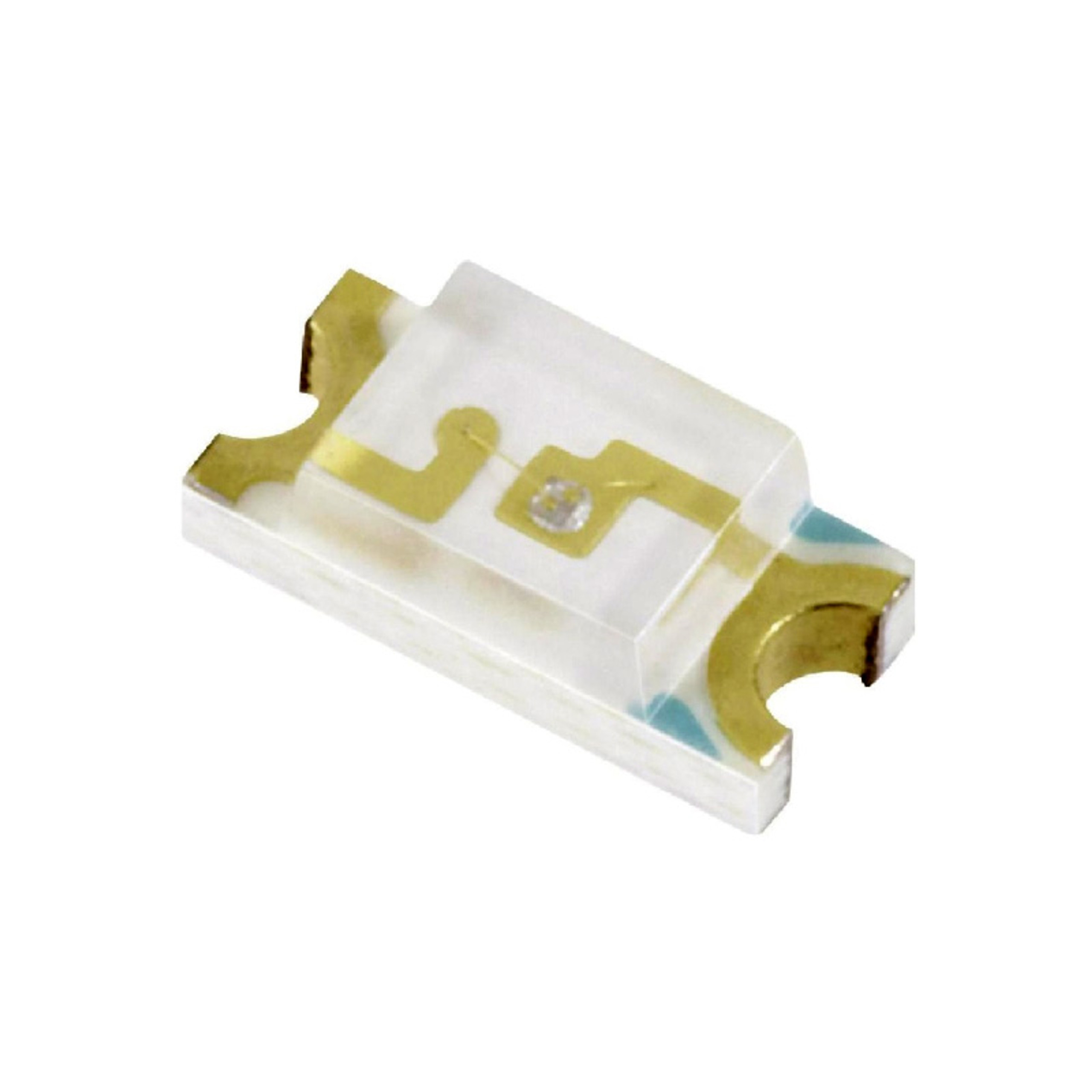 |
| 2 | push button | 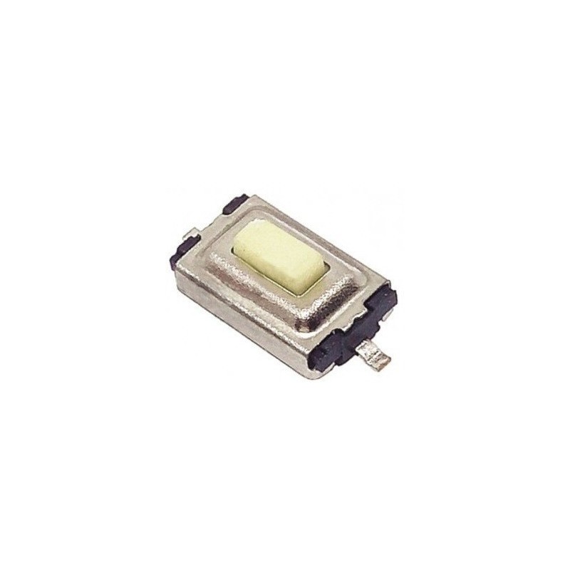 |
| 1 | 4-pin Right-Angle SIL Headers | 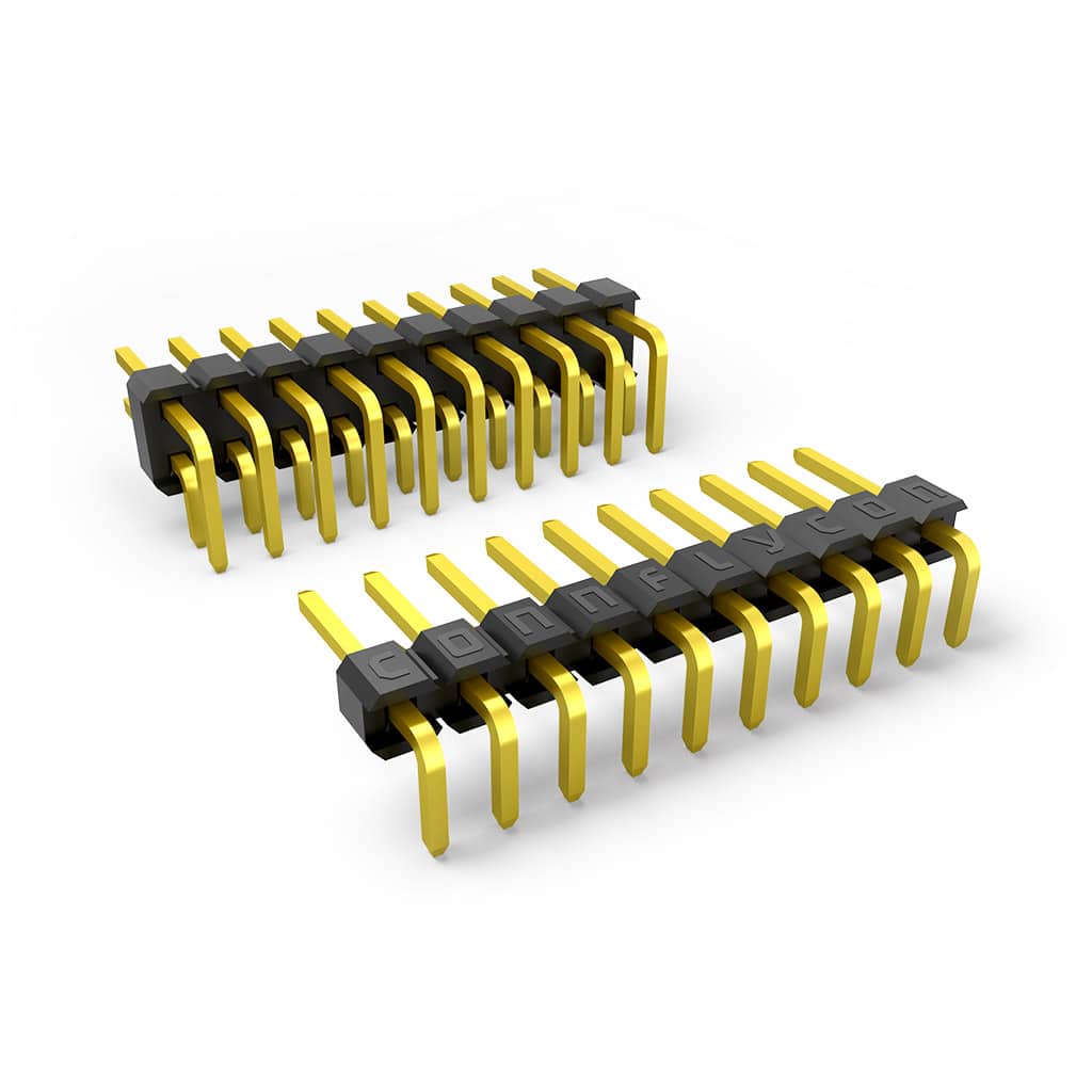 |
| 1 | 3-pin Right-Angle SIL Headers | |
Materials:
| Qty | Description | Image |
|---|---|---|
| 1 | Roll of tin for soldering | 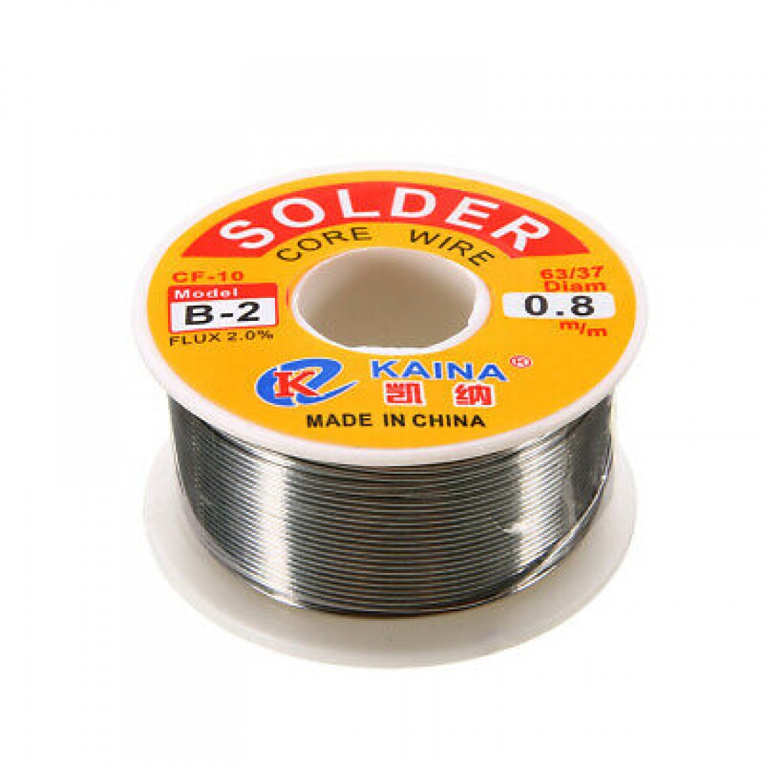 |
| 1 | Soldering iron | 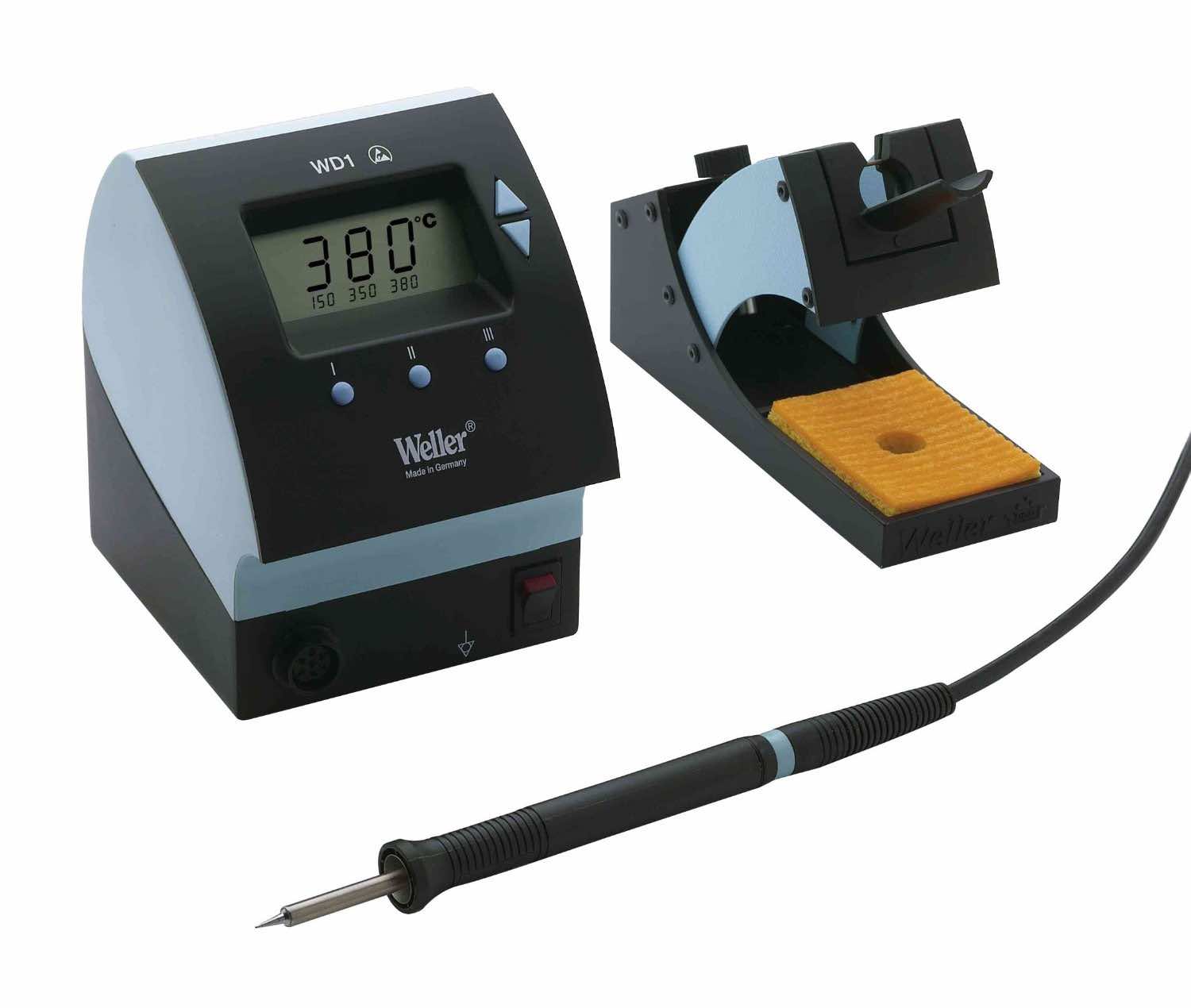 |
| 1 | Tweezers |  |
Pros and Cons of the Process:
Pros:
- Access to specific footprints available in the lab facilitates footprint assignment.
- Exporting the design as SVG from KiCad simplifies parameter configuration in MODS.
- Automated generation of .RML files for the SRM-20 in MODS.
Cons:
- Dependence on the availability and variety of footprints provided by instructors.
- May require manual adjustments in converting the design to SVG.
- Precise configuration needed in MODS to ensure quality of the final result.