8. Electronics Design
Research
Designing a PCB (Printed Circuit Board) using a CNC (Computer Numerical Control) represents an innovative approach that combines the precision of CNC technology with the flexibility of electronic circuit design. This technique enables the fabrication of circuit boards with high-precision traces and components, providing an efficient and customizable alternative to traditional PCB manufacturing methods. The CNC's ability to cut, drill, and engrave materials with great accuracy facilitates the creation of complex and detailed designs, making the PCB design process more streamlined and accessible for engineers and designers.
Here you will find the group assignment with a little more information.
Why did I use KICAD?
I chose to use KICAD because it is free and open-source software, making it accessible to everyone. Additionally, KICAD is very intuitive and easy to use, and it offers a wide range of features, including schematic capture, PCB layout, a 3D viewer, and a comprehensive component library. Furthermore, community support for KICAD is robust, providing abundant resources and tutorials. The ability to work on complex designs without the restrictions of licensing fees is another great advantage, making KICAD a cost-effective solution for PCB design.
Besides KICAD, I also know EAGLE and Altium Designer. EAGLE is known for its powerful features and ease of use, with a large community and extensive library support. It integrates seamlessly with other Autodesk products, which can be beneficial for certain design workflows. On the other hand, Altium Designer is a professional-grade tool widely used in the industry. It offers advanced features such as high-speed design, advanced layer management, and sophisticated simulation tools. Altium is known for its comprehensive design environment and powerful capabilities, making it suitable for complex and large-scale projects. However, its cost can be a limiting factor for some users.
Electronics design
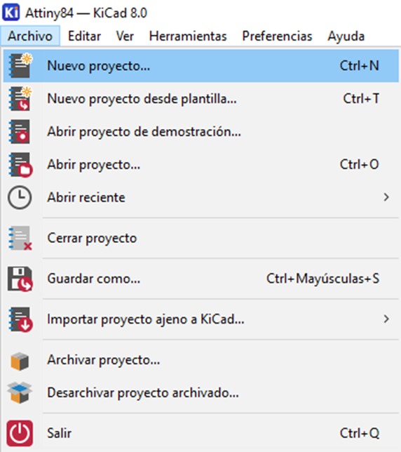
The first step to follow is to open the KiCad 8.0 application. To open a new file, we select the File tab, then New project.
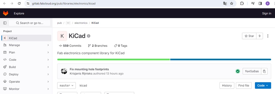
To be able to visualize the electronic components available at FabLab Puebla, it will be necessary to enter the following link , where in the "Code" section, you can download it. I did it in .zip format, which I later decompressed. Additionally, we were recommended not to place that folder in a location where we usually delete things.
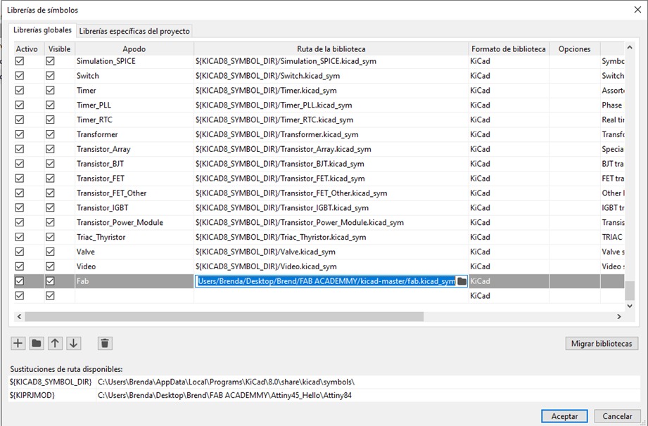
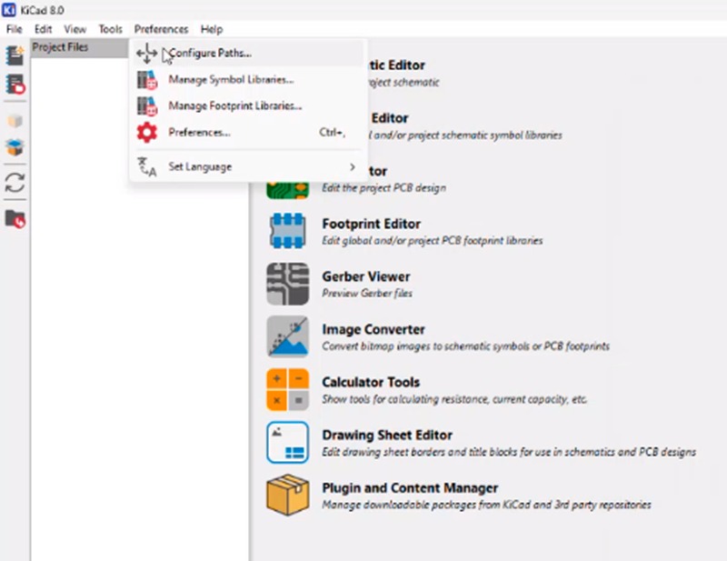
To include the elements in the KiCad application, we select Preferences, Manage Symbol Libraries... This will open a screen where we will select the "+" symbol and enter the name "Fab". Then, we will select the folder where the fab.kicad_sym file is located from the downloaded folder.
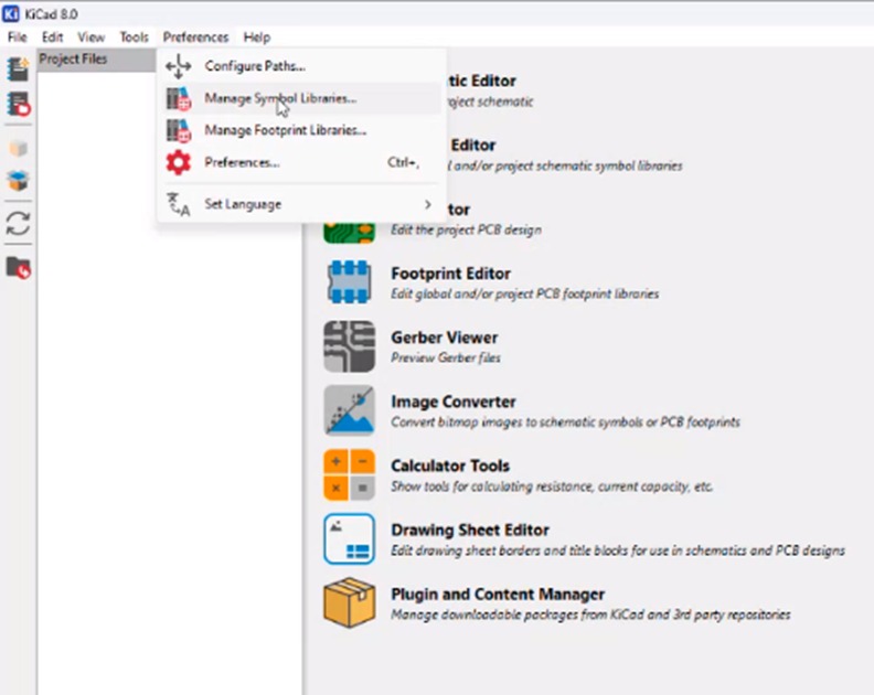
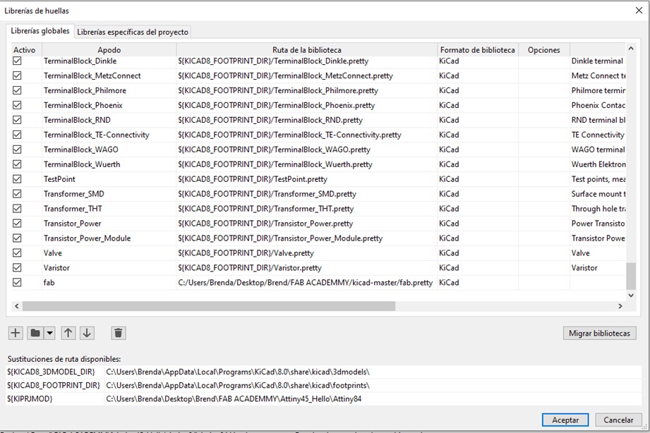
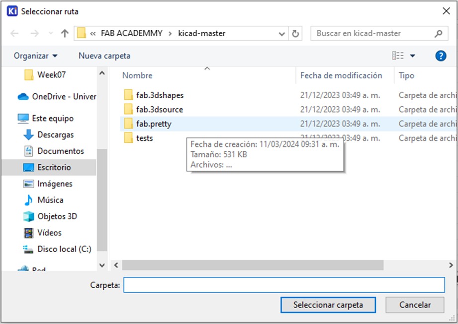
Subsequently, we select the "Manage Footprint Libraries..." option from the preferences menu. It will open a window similar to the previous step. Press the "+" symbol, and this time we will name it "fab" in lowercase because that's how it will find the files. Then, we select the fab.pretty files.
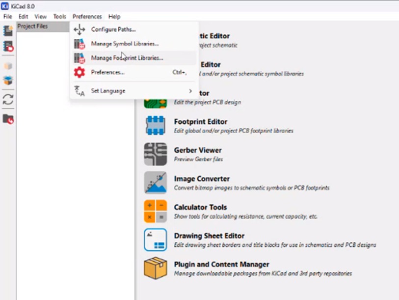
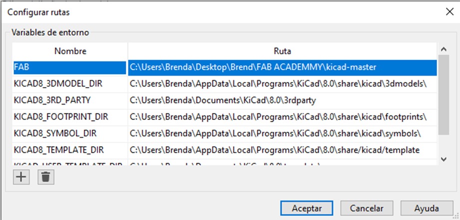
Finally, in the settings section, in the preferences tab, we select "Configure Paths..." where we will input the name "FAB". This time, we will select the entire downloaded folder.
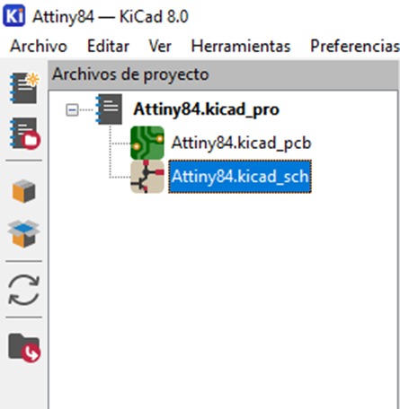
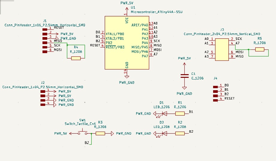
In the project files menu, we will open the one ending in _sch to include all the materials we will use.
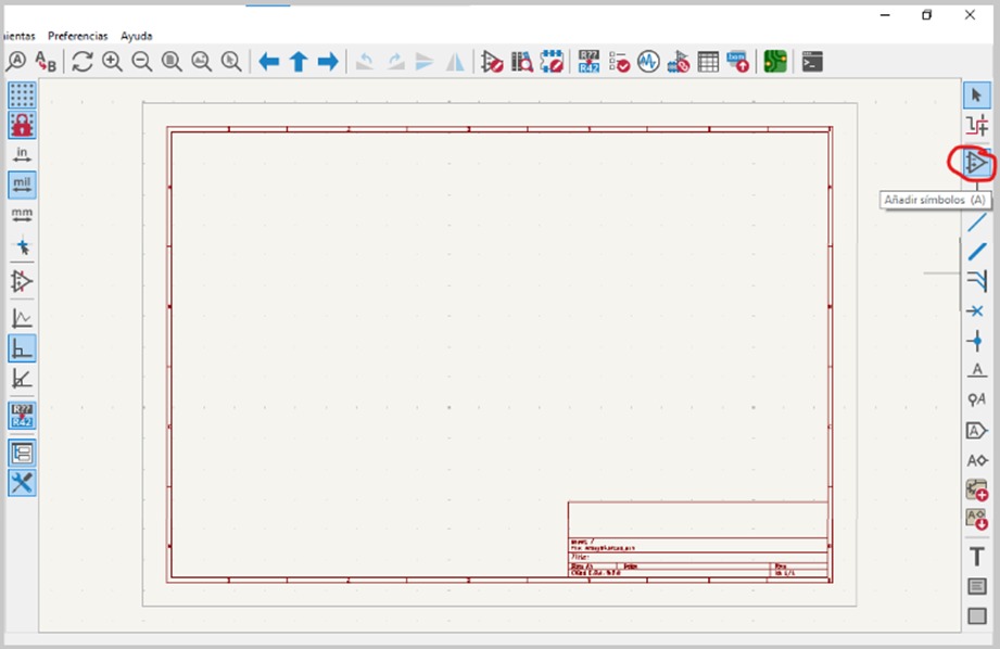
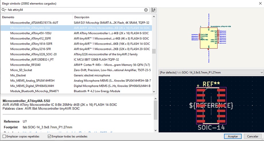
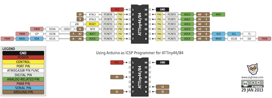
We select "Add Symbols" from the button with the opamp icon, and to search for the component we want, we begin by entering "fab + component name" in the search bar. In this case, I used an attiny44.
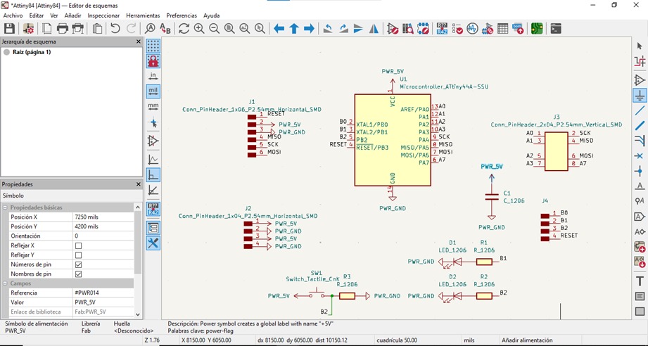
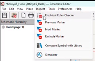
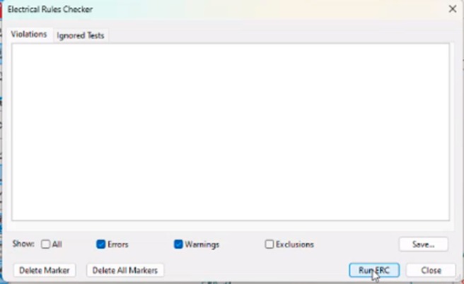
Once all the components to be used are placed and connected as desired, in the Inspect section, we select the Electrical Rules Checker option to see if there are any errors or if everything is in order. In the window that appears, we click on Run ERC, and if something comes up, it needs to be corrected. (It's important not to forget programmer pins and ensure that those placed are of a 2.54 mm size to avoid soldering complications).
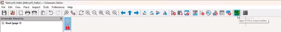
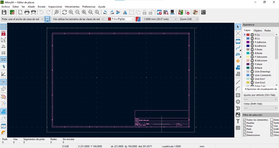
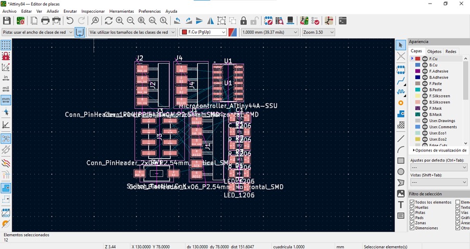
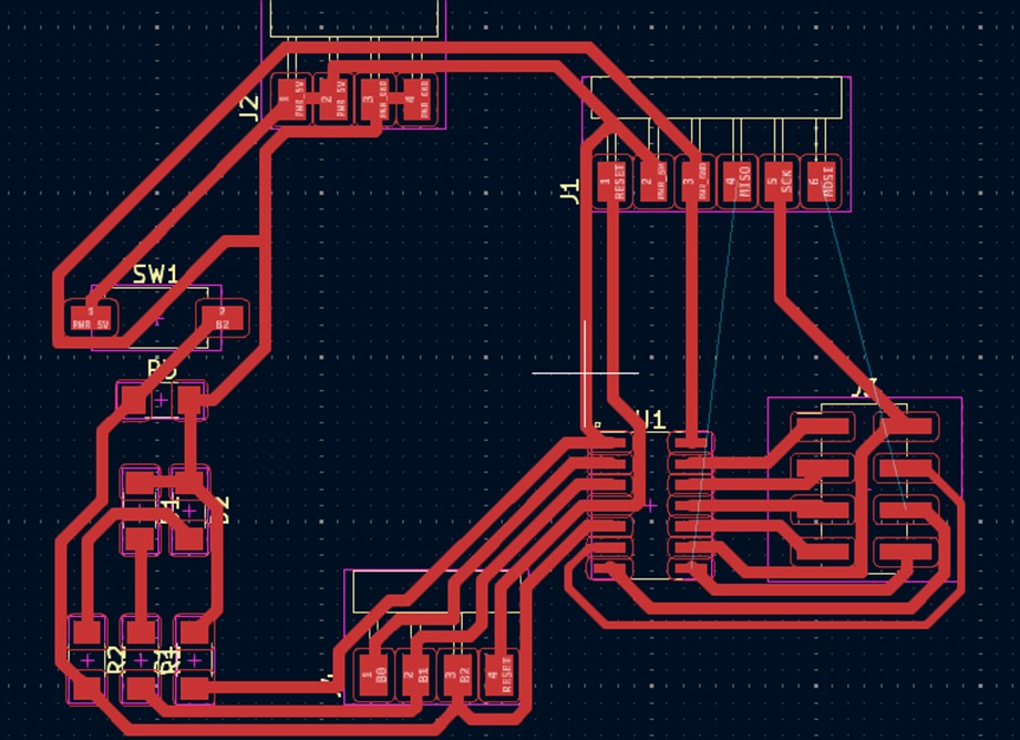
We will move to the component placement design section, where we position the components where they will appear on the PCB. We select the green rectangle drawing, and a screen similar to the one shown will open.
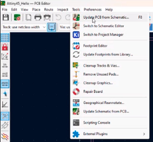
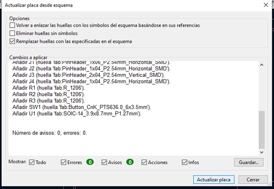
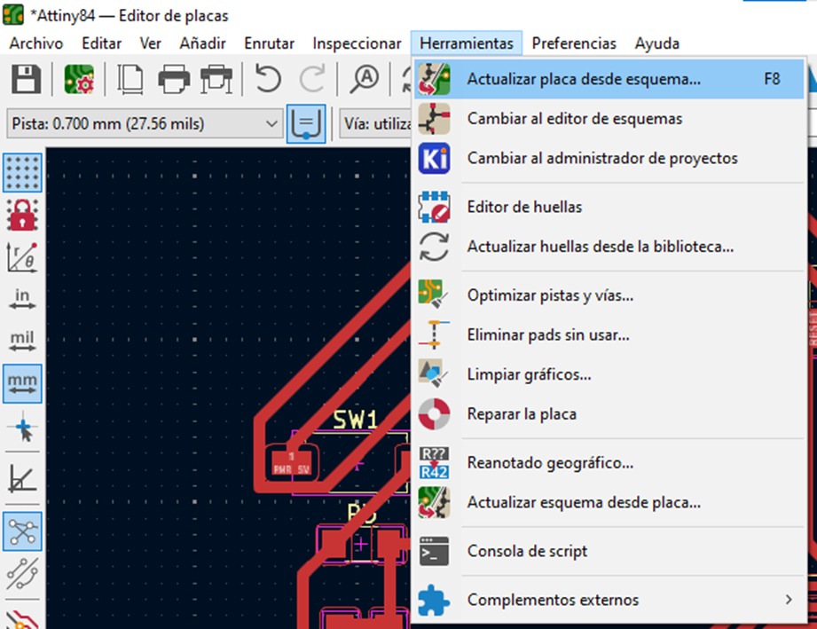
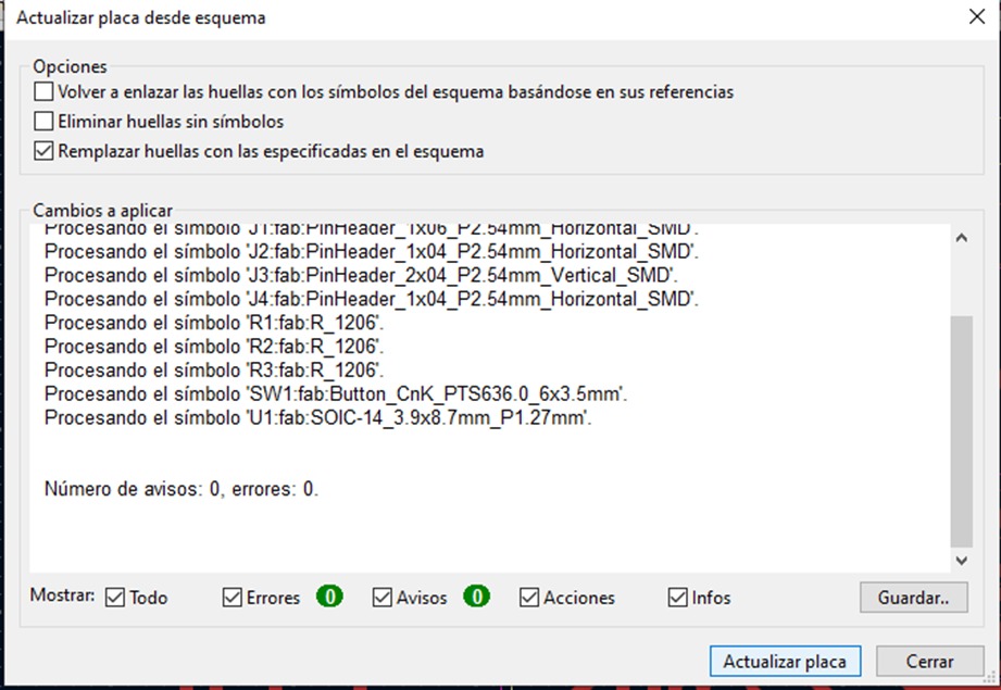
To place the components, in the Tools tab, we select the option "Update PCB from Schematic...". A tab will appear showing a list of components, and we will select the "Update Board" option.
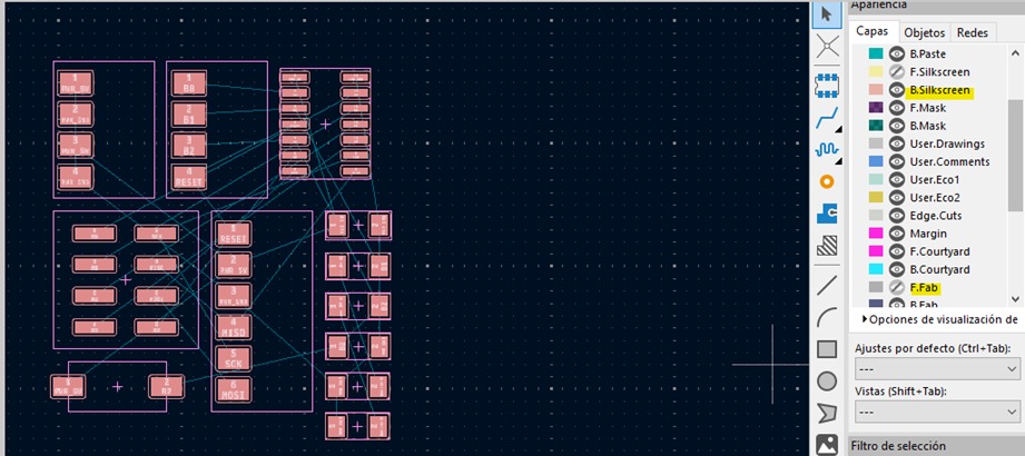
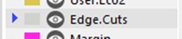
The following layers are important when sending the PCB to a manufacturing company.
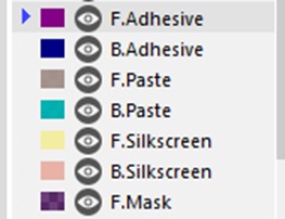
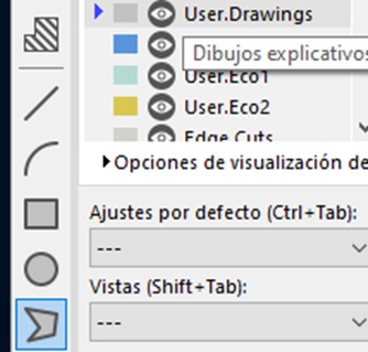
To work in a more organized manner, you can cover the following layers.
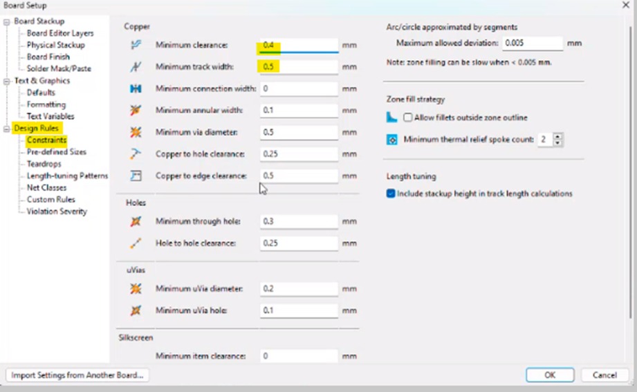
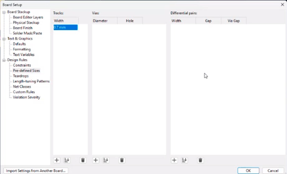
To add the rules for the traces to be made, in the File tab, we select Board Setup... In this section, because the cutting tool has a width of 0.4 mm, we set the minimum separation to 0.4 mm and the maximum to 0.5 mm in the Design Rules section.
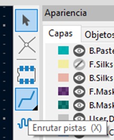
To start laying down the traces, we can select the following symbol or simply press the X key.
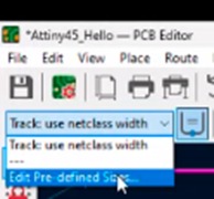
To select the thickness of the traces we will place, in the top section, we will find a dropdown menu where we select "Edit Pre-defined Sizes...". By pressing the "+" symbol, we can add a trace of 0.7 mm, which is recommended to make it easier to work with when soldering.
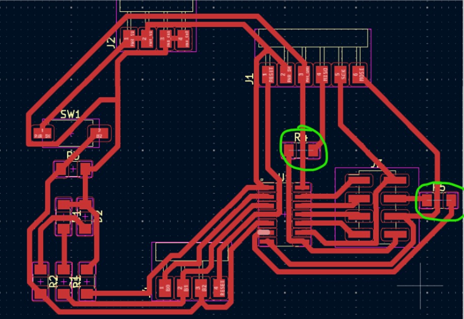
In this case, it became impossible to connect MISO and MOSI. Therefore, a valid option would be to change the connections in the schematic, and then follow these steps: In the schematic, we can place 0-ohm resistors to function as bridges, and then select the "Update Board from Schematic..." option in the tools tab, followed by selecting "Update Schematic."
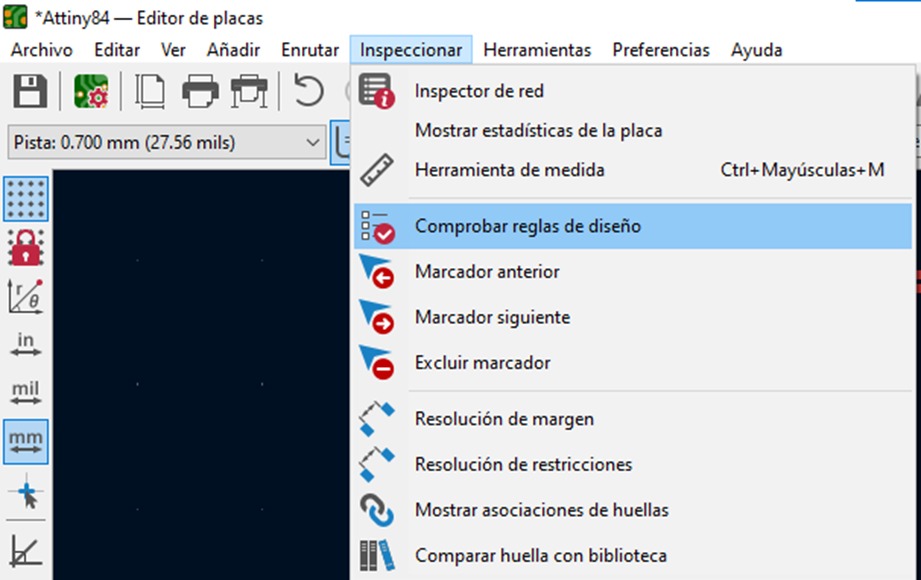
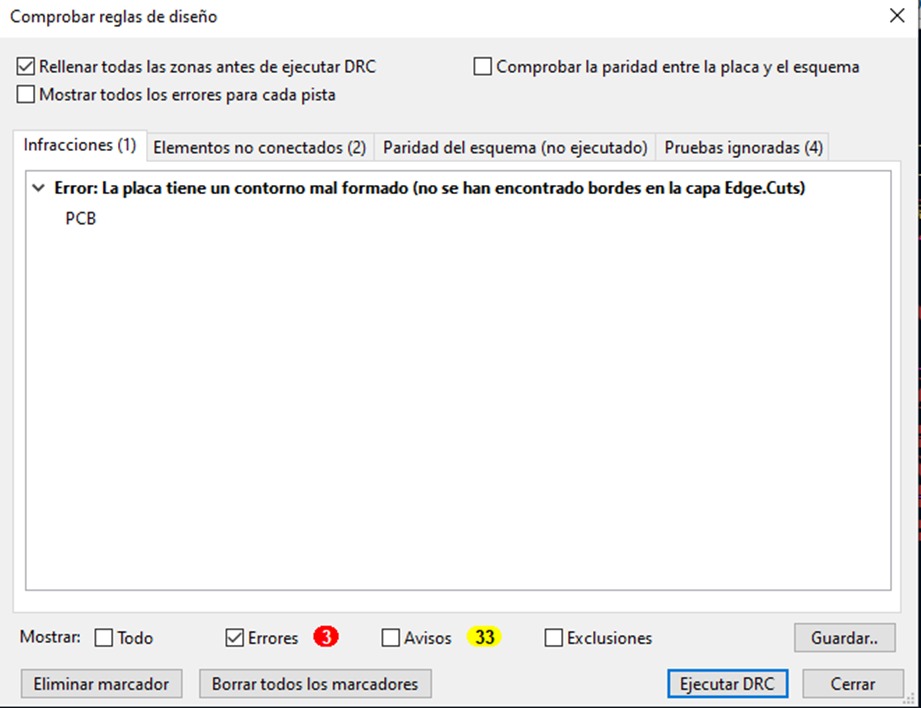
Now, we check for errors in the PCB design in the Inspection section, under the Check Design Rules option. We select Run DRC.
It's important to mention that if you want to add text, it should be done using this option and placed on the copper layer so that it gets cut as well.

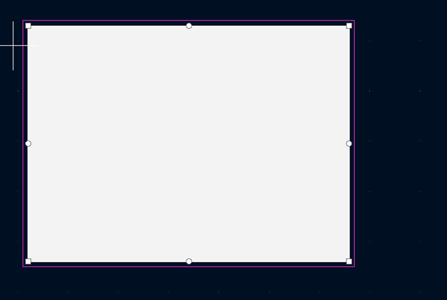
Now, we select the Edge.Cuts layer to create a rectangle outlining the size of the PCB, ensuring that everything is within the shape we created.
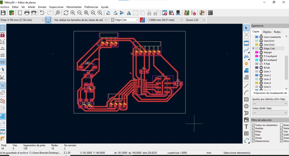
Now, on the Margin layer, we place a rectangle ensuring that there is a 1mm separation between it and the white rectangle created earlier. Subsequently, the white rectangle is deleted, as it is only for reference.

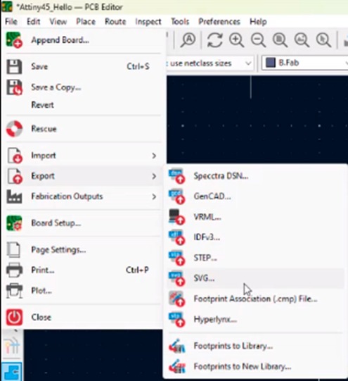
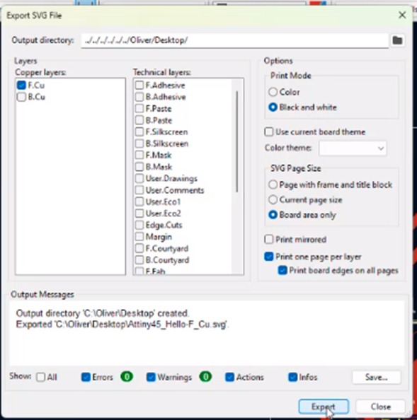
Now, to obtain the layer where only the etching of the traces will be done, in the File tab, under the Export option, we select SVG... We must ensure that in this window, the following options are selected: F.Cu, Black and white, Board area only. Then, we can proceed to export.
Finally, we select the User.Drawings layer and use the polygon tool to create a shape within the purple layer, ensuring a 1mm separation. And to export, we follow the same steps as before, but this time we select the User.Drawings layer.
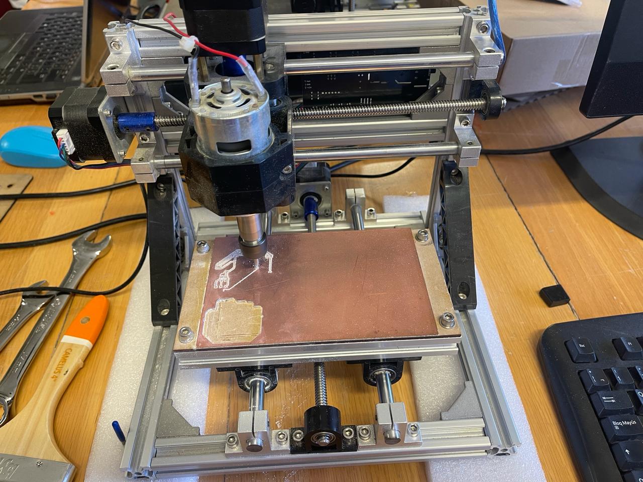
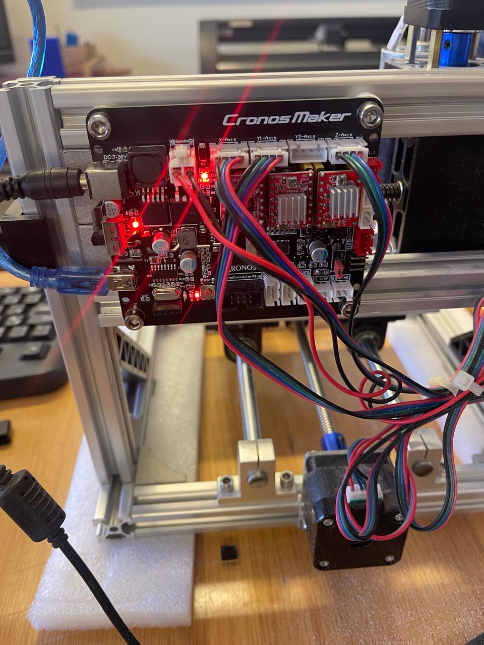
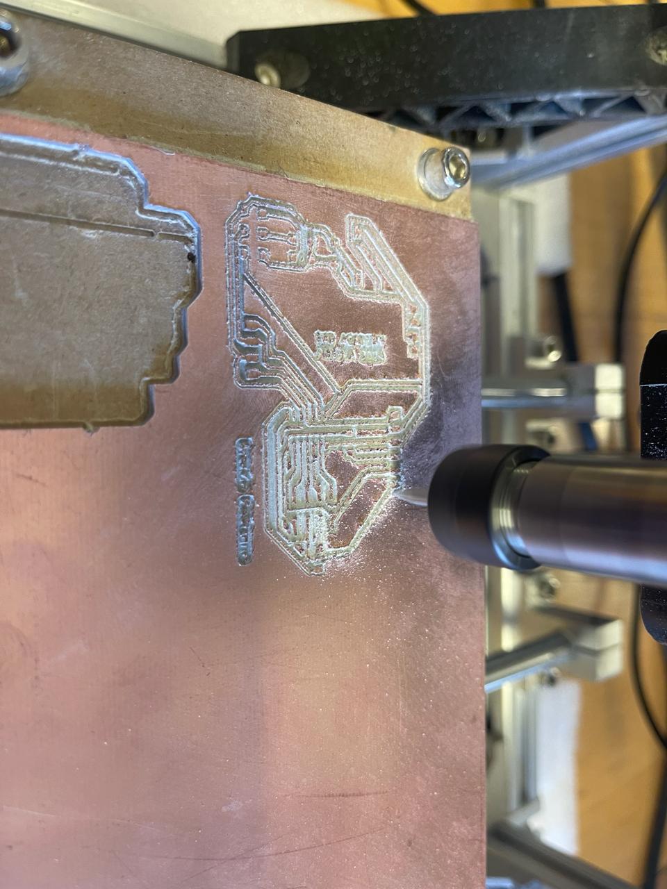
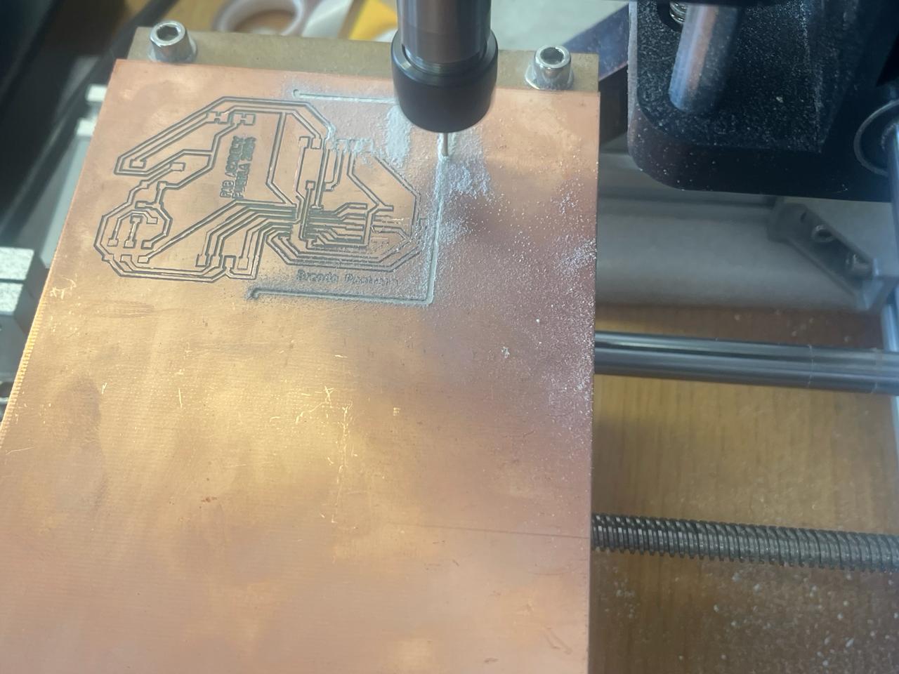
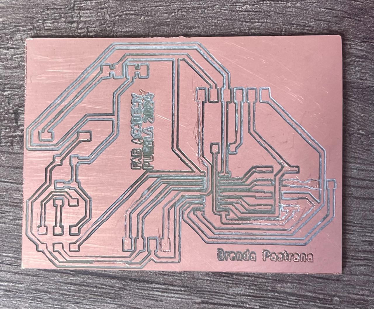
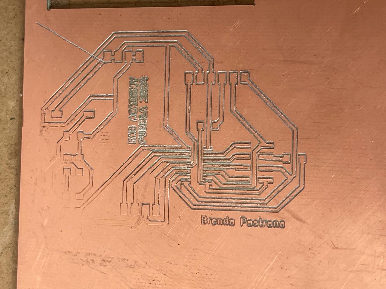
Physical PCB Design
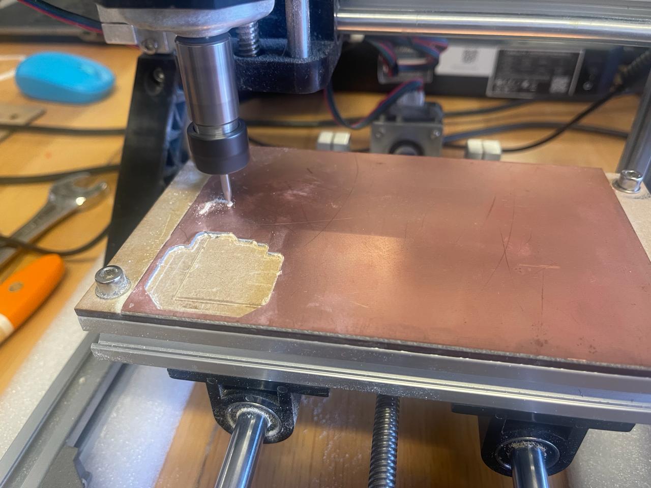
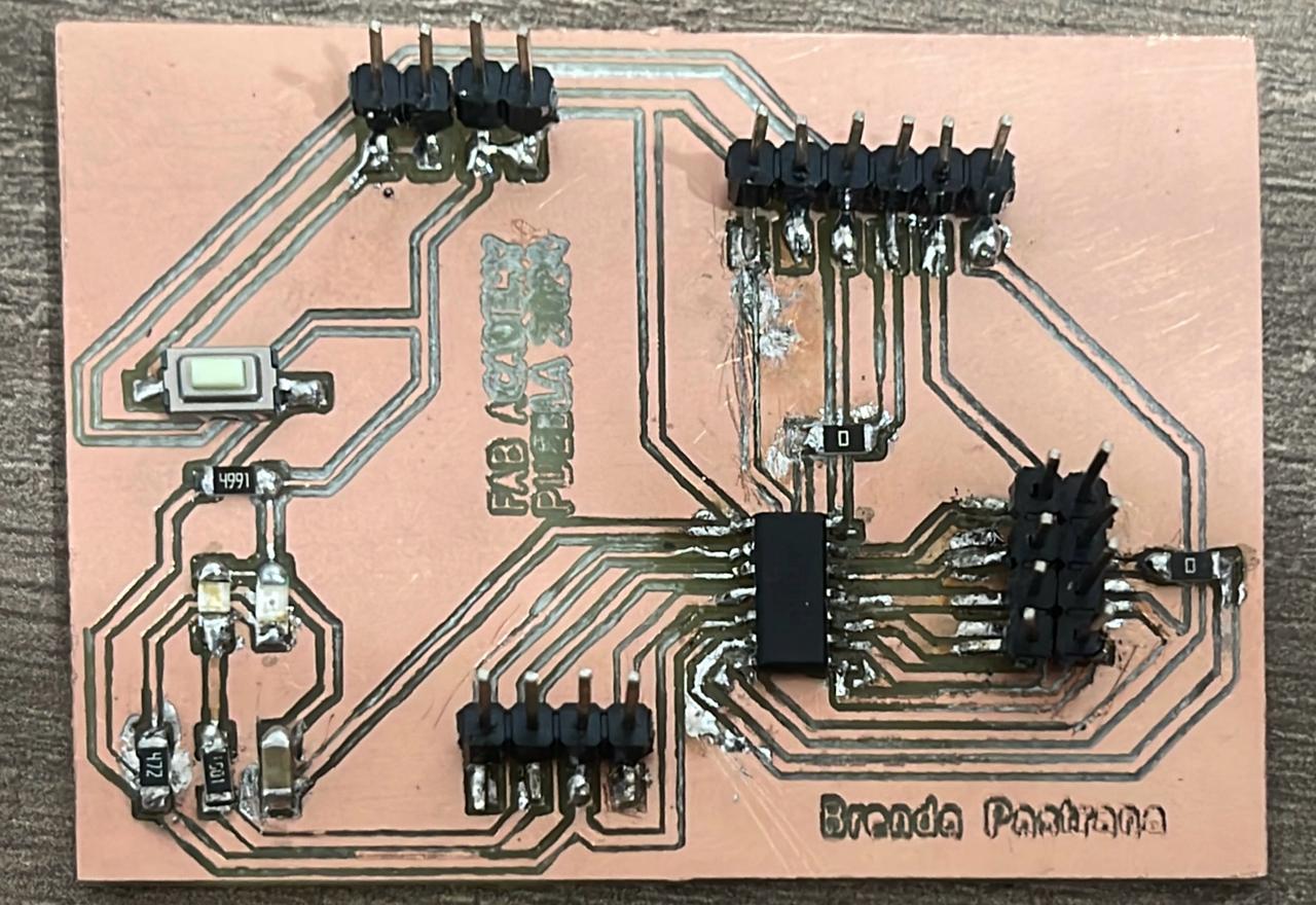
For this part of the physical PCB design, I encountered several complications, which will be discussed further in the Problems section. To cut the PCB, we will make use of the modsproject.org website, which can be reviewed in more detail on week 4 of my website. Once cut, we can proceed to solder the following components:
- 2 resistors 0 ohms
- Attiny 44
- 1 ceramic capacitor 1 microfarad
- 2 LEDs 1206
- 2 resistors 1 kilohm
- Button
- kilohm resistor
- 22 pins
Problems and how I fixed them
One issue I encountered several times was that after finishing cutting, I realized that the traces were not properly made because the tool didn't lower correctly. Later, I discovered it was because the tool was no longer sharp.
Another important point is that when I initially made the traces too thin, the tool lifted them. I had to redesign them to be wider. I recommend making them 0.8 mm in track width to avoid this issue.
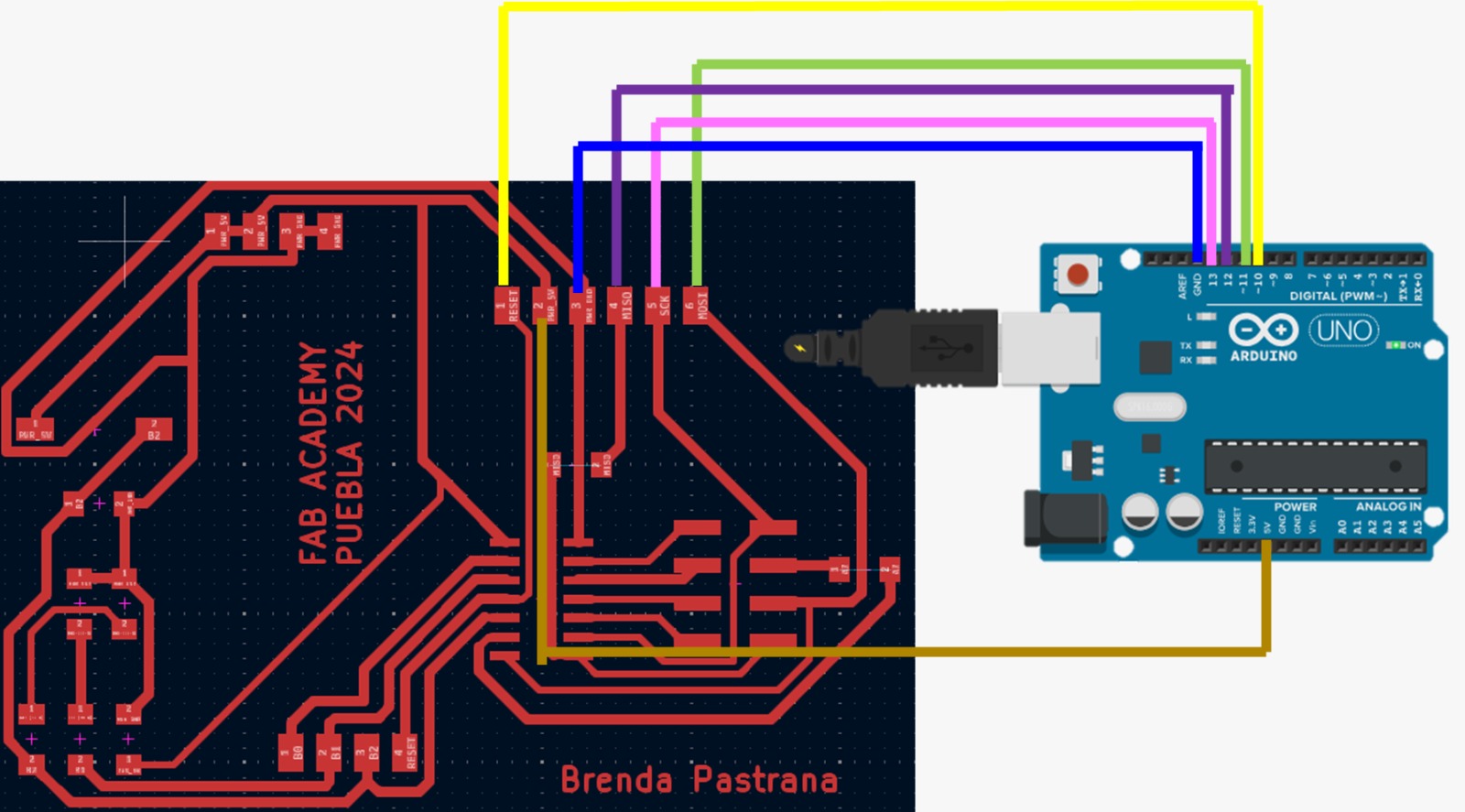
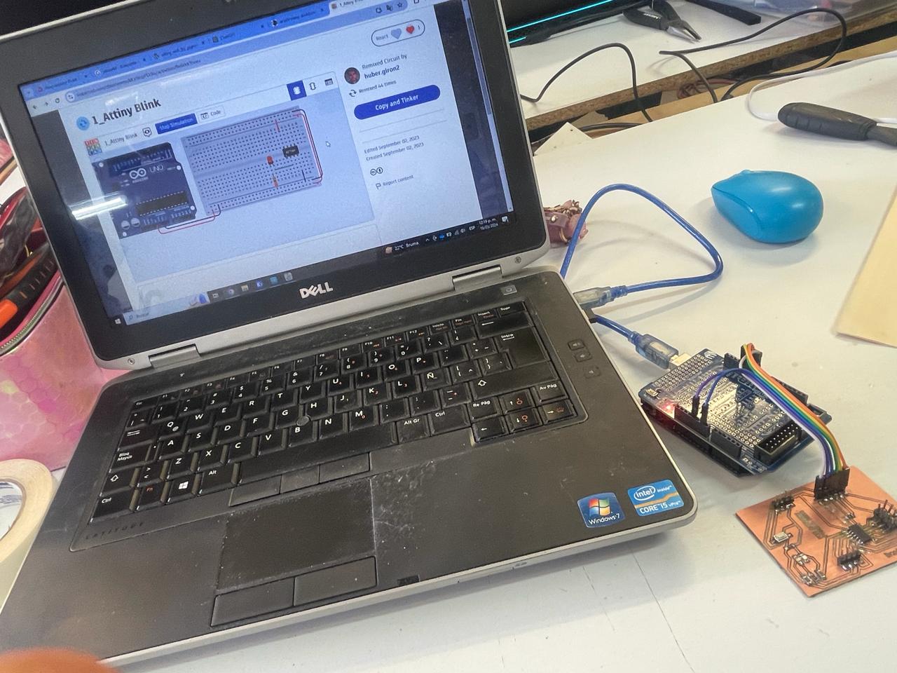
To program it, I used an Arduino Uno as an ISP.
Lastly, when attempting to program the PCB, I noticed that the LEDs weren't lighting up properly. One had a very dim light, and the other didn't light up at all. Upon further examination, I realized that when designing, I accidentally connected the button with one of the LEDs, causing the LED's resistance and the button's resistance to add up. This prevented the LED from emitting light. My solution was to use a cutter to sever the trace connecting the pin to the button, ensuring that the resistances did not sum up anymore.
Conclusion
At the end of this assignment, I believe it is important to emphasize the necessity of understanding design rules to avoid errors. It is essential to pay close attention to the elements being placed; for example, pins have different spacing distances, so the choice will depend on which ones you need to place. Additionally, you must consider the values of the resistors for each component, as you cannot use the same resistor for a button as you would for an LED.
For more information on how to measure resistance with a digital multimeter, you can consult the article How to Measure Resistance with a Digital Multimeter. This article explains step-by-step the process of measuring resistance, including how to prepare the multimeter, how to correctly connect the test leads, and what to expect on the device's display. Additionally, it provides useful tips to ensure accurate measurements and avoid common mistakes.