
4. Electronics Production
This week, I machined my own Printed Circuit Board (PCB) from a copper-clad sheet, then I learnt the basics of how to solder components onto it and ran diagnostic software to ensure that all components were properly soldered and functioning correctly.
Group assignment:
Group Assignment for week 4, Fab Puebla.
Milling your own Printed Circuit Board:
I divided this section into 3 parts: digital file preparation, creating an RML file and the actual milling process.
Digital file preparation:
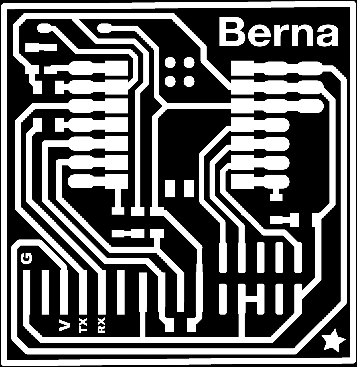
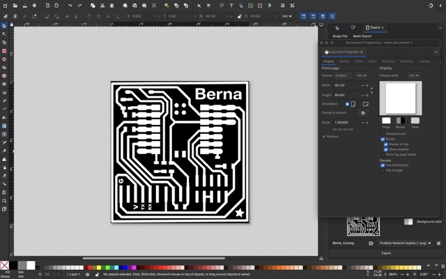
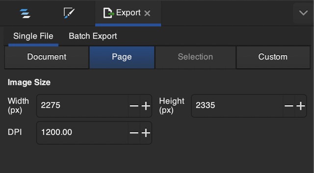
The first thing we had to do was figure out what pattern we wanted to cut, we received a template as a PNG image but I decided to slightly modify it to make it a little more unique and to practice exporting images correctly, so I replaced the logo at the top with my name and added a small star in the bottom corner. Initially, I tried to do this by simply importing the image into Procreate, covering the original logo, and replacing it with my name and then exporting it as a PNG. Unfortunately, when I imported it into modsproject.org, the dimensions were off. I eventually traced the problem back to the DPI, despite the resolution remaining the same, the absolute size of the image changed.
 Let's explore the PNG export process in greater detail to prevent sizing issues during the milling
process. The concept of image resolution is relative, which means we need to provide the milling
machine a specific reference for it to determine the absolute size of your circuit board. In this
case we will use DPI (Dots Per Inch) as a reference. For example, if the template you're working with
has a DPI of 1200, your PNG file needs to align with this DPI to preserve the intended dimensions.
By the way this precision is necessary to ensure all components fit correctly on the board. To illustrate
this concept more simply, I've created an illustration that demonstrates how an image with the same
resolution may vary in absolute size when printed, or in this case, milled depending on the DPI used.
Both of these images have the same resolution, but one has twice the DPI of the other making it half the
absolute size of the other, one being 1" wdie and the other 2".
Let's explore the PNG export process in greater detail to prevent sizing issues during the milling
process. The concept of image resolution is relative, which means we need to provide the milling
machine a specific reference for it to determine the absolute size of your circuit board. In this
case we will use DPI (Dots Per Inch) as a reference. For example, if the template you're working with
has a DPI of 1200, your PNG file needs to align with this DPI to preserve the intended dimensions.
By the way this precision is necessary to ensure all components fit correctly on the board. To illustrate
this concept more simply, I've created an illustration that demonstrates how an image with the same
resolution may vary in absolute size when printed, or in this case, milled depending on the DPI used.
Both of these images have the same resolution, but one has twice the DPI of the other making it half the
absolute size of the other, one being 1" wdie and the other 2".
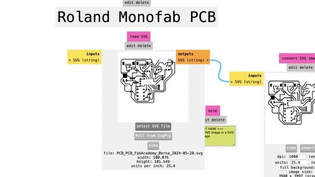
Creating an RML file
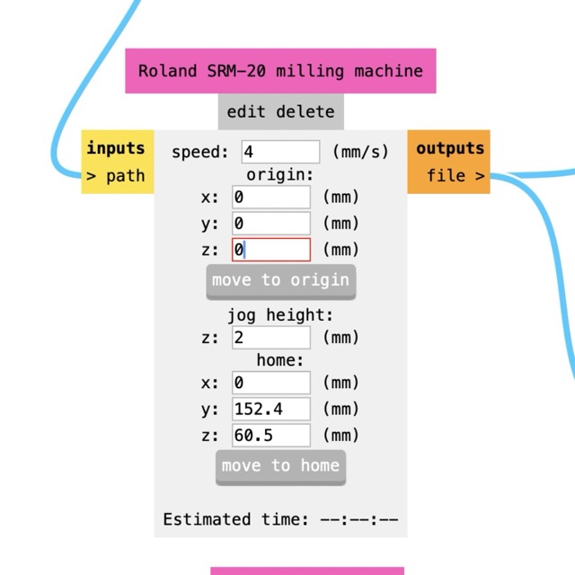
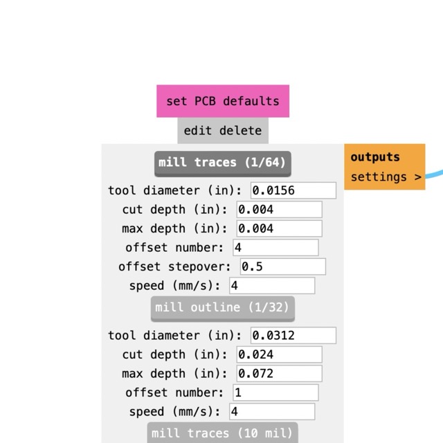
We used an online node based program called modsporject to convert the SVG file we exported from Kicad into G-code for milling, here are the steps we took:
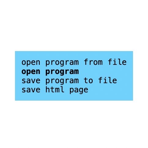
1.Opening mods project and choosing milling machine:
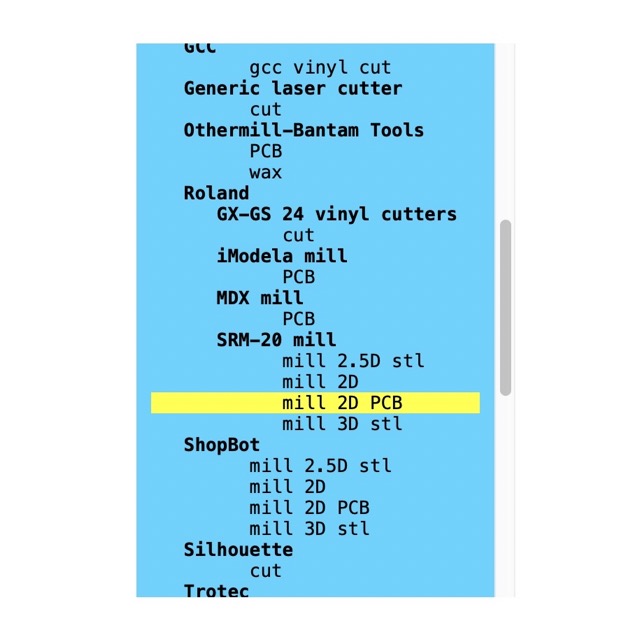
2. Main interface:
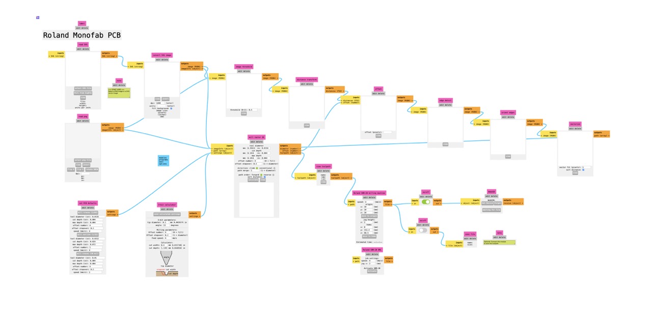
3. Here you need to selcect your SVG:
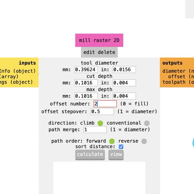
4. Then you select soffset numbers, 2 in this case, then set the origin to 0 for x,y and z and finally just click mill traces at 1/64th.
The actual milling process:
In order to cut all the way through the copper-clad sheet without worrying about hitting the metal base, we laser-cut an MDF sacrificial board which matched the dimensions of the base. We then used double-sided tape to secure the copper-clad sheet to the board and mounted it on the CNC mill using four screws.
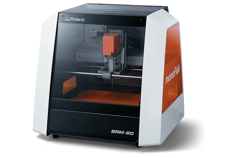
Properly attaching the bit to the CNC mill is essential for precision so I inserted the bit into the spindle up to the point where only the part of the bit that is fully cylindrical and at its widest remains exposed. I did this to insure that the bit was as short as possible outside the spindle, which significantly improves the stability and accuracy of the cut. Next, I tightened it down with a hex wrench, securing it firmly in place to prevent any movement during the milling process. To avoid any damage or dulling of the edge, I made sure the bit didn't drop as I secured it. This process was key for producing clean and precise cuts. We also used two different bits, one for engraving and one for the final cut.
Then came setting the origin, setting the xy origin was pretty straight forward, you just need to move the bit all the way the bottom left corner click the xy origin button. Setting the Z axis is a little more involved, specially since different people do it differently. Some of my classmates used a piece of paper to make sure the z origin was as close as possible to the surface, I turned the spindle on and lowered it slowly until i saw that the bit was slightly cutting into the material, a little like using pulse in a laser cutter. The reason i did this is to make sure I didn’t dull the bit when pushing it down into the copper clad sheet. I was advised to do this by a collegue, if you know of a better way to do it or a reason why the method I used leads to worse results please let me know, I want to learn.
After this it was simply a matter of removing the PCB from the base and removing the double sided tape. I decided to sand the edges a little bit to make sure they werent too sharp and then used alcohol to clean the surface to make sure it was easy to solder. Of course I also made sure to clean the machine using a vacuum machine to remove the dust and removed my sacrificial board.
Equipment requiered:
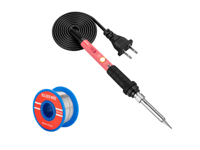
To solder there are some essential elements and others which aren't strictly needed but can make the whole process much easier. The essential ones are a soldering iron which is a tool with a metal tip which heats up to allow you to melt solder, and the other is as you might expect, solder wire which is a metal alloy with a relatively low melting point and is used to make metalic connections between components, that's it.
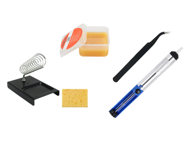
Non essential (but really useful) equipment include a silicon soldering mat which helps you in keeping everything organized and since it's less slippery than the table it holds your PCB in place, next is a small box with compartments where you can keep your components, this helps you stayed organized too. There are also tools that will help you with the actual soldering and that includes tongs, magnifying glasses, tweezers to hold components, actually tweesers are kind of essential equipment now that I think about it, you can also use a device which helps you remove excess soldering paste by sucking it up with a vacum and finally a wet sponge for cleaning the soldering iron and soldering paste which I only discovered after my third PCB
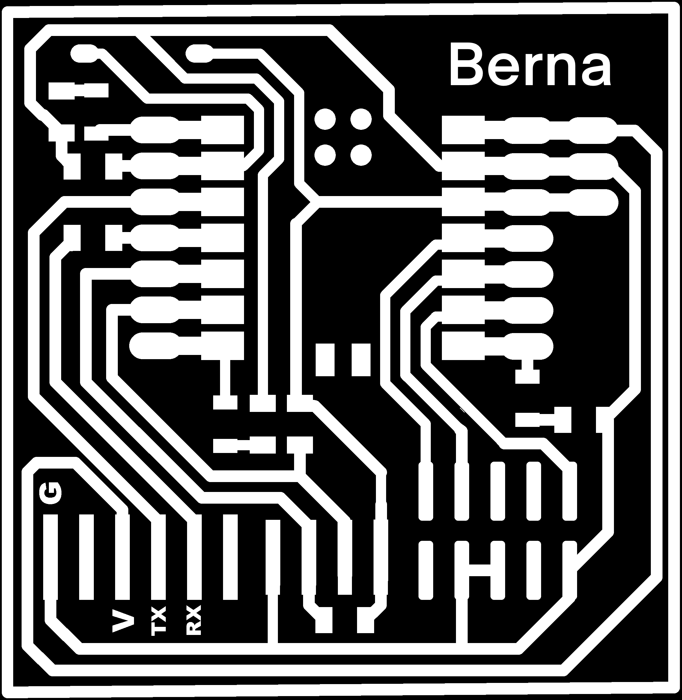
Using PCB map as reference for soldering:
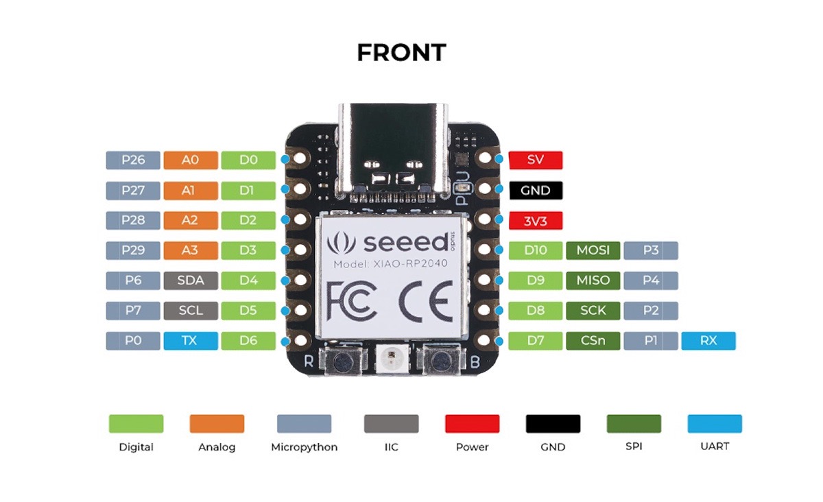
To know what components you will need and where to solder each one you need a reference, for this you can use both a schematic and an actual image of the PCB layout as it will look in the final PCB. In this case I used the one that was provided to us and I also used a pinout diagram to know which pins had specific functionalities like SCK, MISO, MOSI or reset for example.
The actual process of soldering:
I had never soldered before, I had used soldering irons to melt plastic and such but never to solder PCBs. Initially it seemed daunting but it turns out it's not that hard when you take your time and use relatively large components like I did. What I belive helped me the most was was understanding how soldering moves from one surface to another and why, I started by heating the solder wire directly which lead to large blobs of solder that wouldn't stick to the surface I wanted them to. I then understood that solder won't flow to cool surfaces so I changed my technique to heating the actual point the PCB where I want to solder and then only touching the solder iron slightly with the solder wire leading to an even distribution of solder.
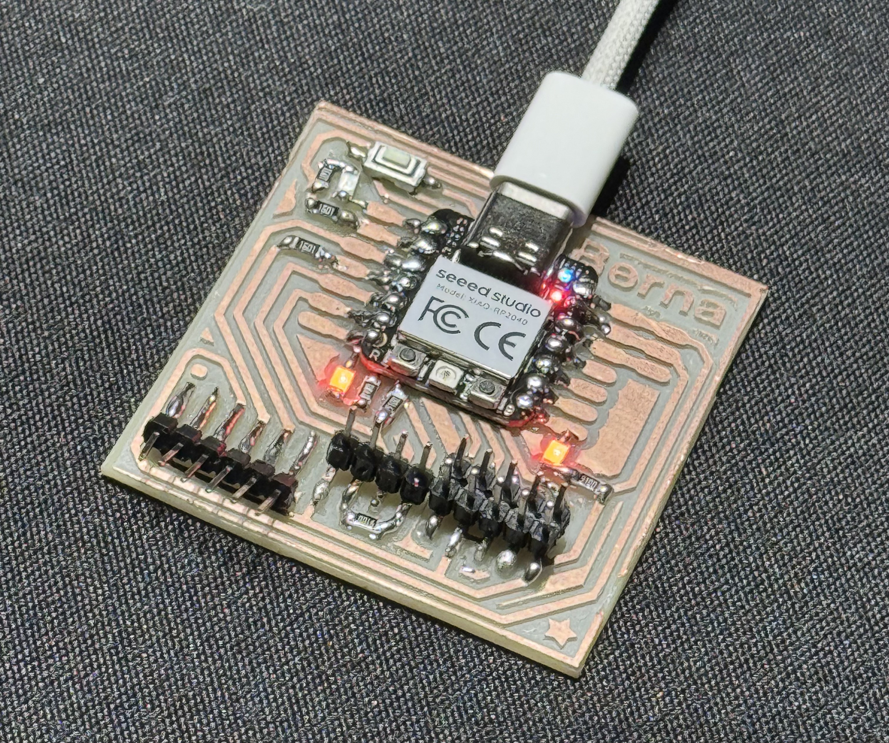
Final product:
I was very satisfied with the final product. I want to make my own functioning prototypes so liked two things in particular about my PCB. One was the fact that I managed to make a small and compact PCB, specially in comparison to a regular Arduino Board, and the second was the cost, my ATtiny was only a couple cents vs 20$ for my Arduino. One of the reasons I signed up to FabAcademy was the fact that if I ever want to make a small batch of products, for example a small project funded by a crowd funding campaign, I wouldn't be able to use an arduino. One of the reasons is it would give off a DIY look which won't give the customers much confidence, but that's not the main problem. Imagine a relatively small batch of 2000 products, the cost difference between a small DIY PCB with a 30 cent ATtiny and a 20$ Arduino board might be 18$ per unit. That's 36,000.00$. Having the ability to design my own custom PCBs would allow me to create smaller products and save tens of thousands of dollars whcih could be the difference between the product existing or it being just a dream. Specially if the final product is intended to be cheap, say less than 50$, 18$ per unit is almost 40% of the cost, that would take all the profits I could expect to make from the sale.
Software & testing:
This section is divided into the process of testing the soldering with a potentiometer and then running the arduino code to make sure it all works
Multimeter Testing for Continuity and LEDs
I used a multimeter, not a potentiometer, to test the continuity of my soldered connections on the PCB. To perform the continuity test, I set the multimeter to the continuity setting, which beeps when a complete circuit is detected. This involves placing the negative (black) probe on one side of the connection and the positive (red) probe on the opposite side. If the multimeter beeps, it indicates that electricity can flow through, confirming the connection is intact. If there is no beep, it suggests a break in the connection.
Additionally, I used the multimeter to test the functionality of the LEDs. By switching the multimeter to diode mode and applying the probes correctly—positive to the anode and negative to the cathode of each LED—I could check if the LEDs lit up. This not only ensured that they were properly soldered but also verified that they were still functional and not burnt out. This method was particularly useful as it helped confirm that the components weren’t as fragile as one might expect based on their size.
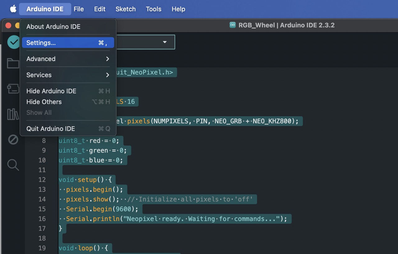
Arduino IDE boards manager setup:
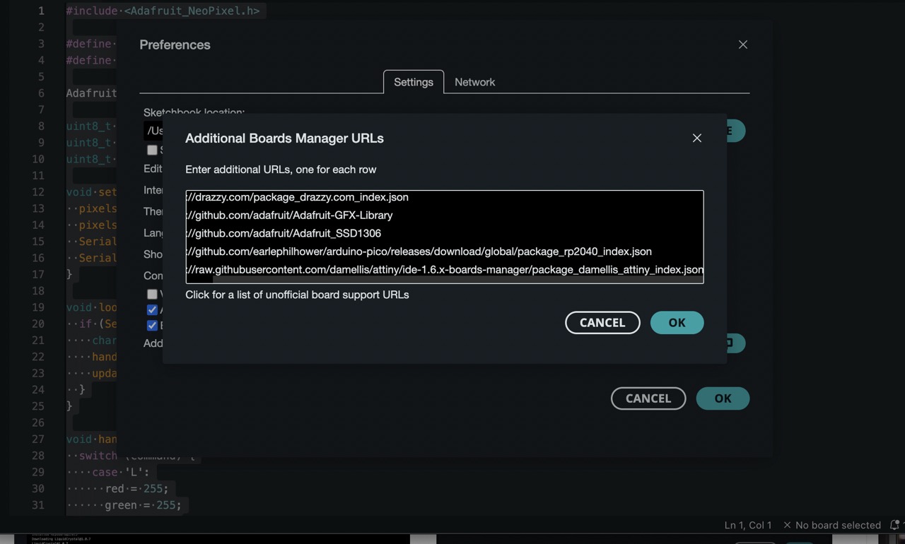
To integrate and utilize the Seeed Studio XIAO RP2040 board with the Arduino IDE, you’ll first need to configure the IDE to recognize this specific board. Begin by launching the Arduino IDE and navigating to the Preferences window accessible through the File menu. In the Preferences window, there is a specific section labeled ‘Additional Board Manager URLs’, where you must input the URL required to fetch the board’s package information: https://github.com/earlephilhower/arduino-pico/releases/download/global/package_rp2040_index.json. After adding this URL, confirm your changes by clicking ‘OK’, which will save the new settings.
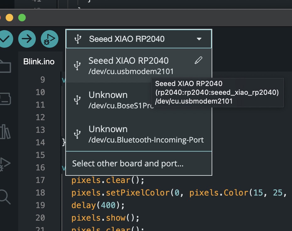
Next, it’s crucial to restart the Arduino IDE to ensure that the new board configurations are loaded correctly. Post-restart, open the Boards Manager from the Tools menu. Here, you should now be able to locate the Seeed Studio XIAO RP2040 by searching for ‘RP2040’ in the search bar. Once found, proceed with the installation of the board package. This package enables the IDE to compile and upload programs specifically tailored for the RP2040 board.
After the board package installation is complete, the final step involves connecting your board to the computer. Once your board is connected via USB, return to the Tools menu and select the appropriate port — typically, this is the port where your Arduino Uno board is connected. By selecting the correct port, the Arduino IDE can communicate with the Seeed Studio XIAO RP2040 board, allowing you to upload sketches and perform tests directly from the IDE. This setup not only simplifies the development process but also ensures you can efficiently troubleshoot and deploy applications on the RP2040 board.
Here is the code we were given to confirm our board was fully functional and properly soldered. It makes the inbuilt NeoPixel on the Xiao ligiht up and cycle between different colors.