Electronics Design
Throughout this eighth week of FabAcademy we will create our own electronic design on a board that we will have two assignments as in the last weeks, a group assignment and an individual assignment. The group assignment is use the test equipment in your lab to observe the operation of a microcontroller circuit board (as a minimum, you should demonstrate the use of a multimeter and oscilloscope) and document your work on the group work page and reflect what you learned on your individual page.
For individual mapping, we need to use an EDA tool to design a development board to interact and communicate with a built-in microcontroller.
what is an electronic design?
An electronic design refers to the process of creating a schematic representation or blueprint for an electronic circuit or system. This includes everything from conceptualizing the functionality of the circuit to detailing the specific components, connections, and layout necessary to achieve that functionality. Electronic designs can range from simple circuits like those found in household appliances to complex systems like microprocessors or integrated circuits.
Having the concept that is the electronic design, it is time to choose the EDA that I will occupy for this assignment which will be KiCad.
KiCad
KiCad is an open source software package mainly used for electronic design automation (EDA). Provides tools for schematic capture, PCB design and Gerber file generation. KiCad is widely used by students and professionals alike to design electronic circuits and systems.
What will I do for my electronic design?
After a long investigation about what I could do for this week, I decided to make a board with a direct USB input, after some research I found that it is not the first time that someone else made this type of USB-shaped PCB, so I started designing my PCB according to what I wanted.
The first thing I did to start designing the PCB was to create a new project in KiCad, this project I called "USB", having created the project I started to do my schematic design. Once inside the schematic I started looking at the components I was going to be using, these components were these:
| Qty | Component | Schematic image |
|---|---|---|
| 1 | Microcontroller ATtiny45V | 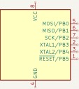 |
| 1 | ISP |  |
| 1 | USB Plain |  |
| 1 | Capacitator |  |
| 2 | Diode |  |
| 2 | Led |  |
| 2 | Power 5V |  |
| 2 | Ground |  |
| 6 | Resistor |  |
| 16 | Pin | 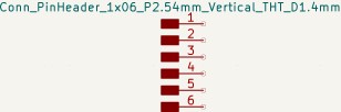 |
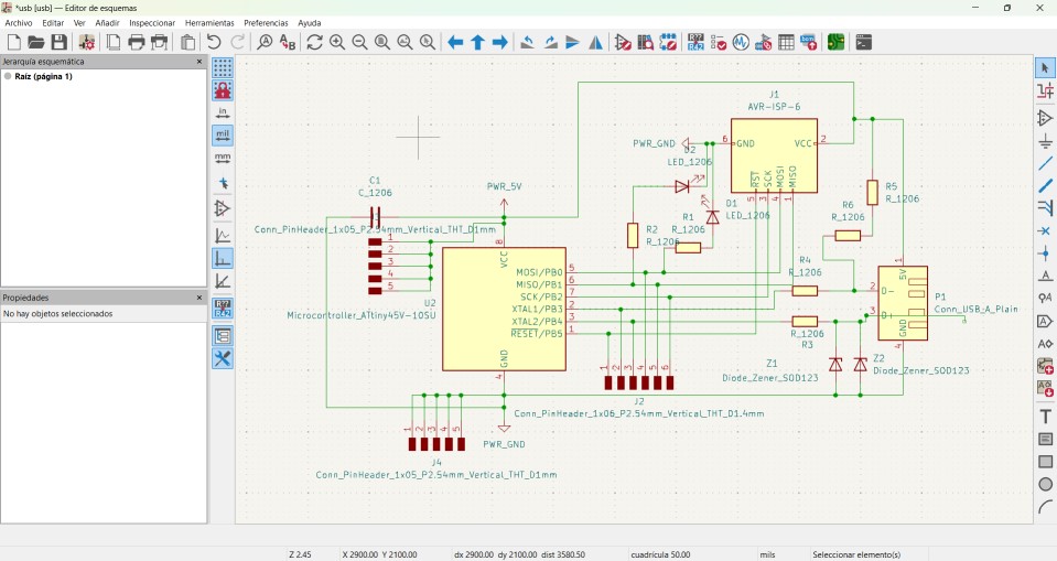
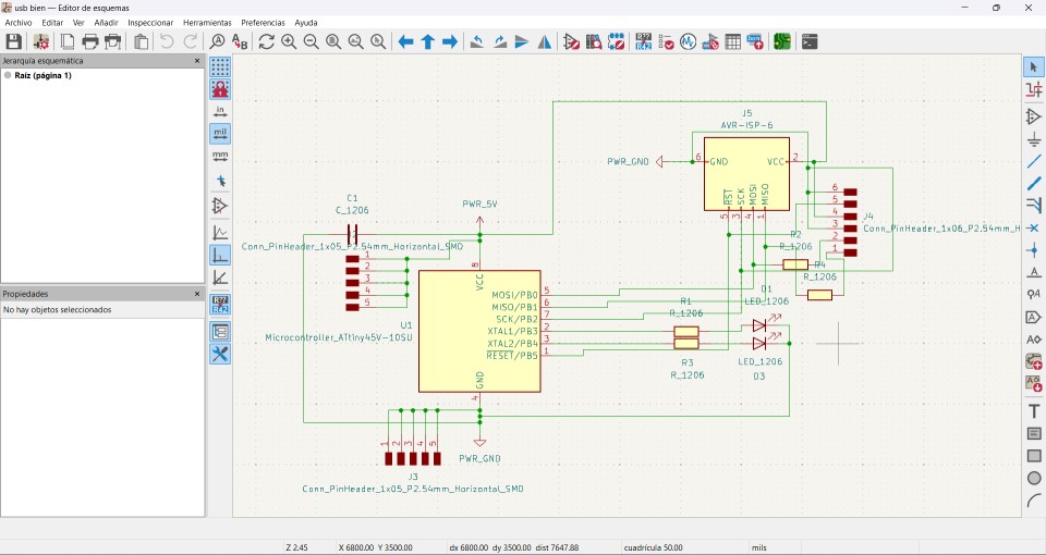
Knowing already the components that I was going to use to build the PCB, I had to make sure that the University had them, in case of not having them I would have to buy them in an electronic components store. Fortunately, they had all the components that I was going to use, so I started making the circuit and then going through my advisor and making sure that everything is correct. This is the circuit I created:
After the review my advisor gave me there was no problem with the circuit, so it’s time to move from schematic to a PCB. In KiCad to move from a schematic to a PCB you have to click on the green button at the top right of the program.
After opening the PCB editor, we have to go to the tools section and select the option to update board from schematic, or simply (depends on your computer device) press the F8 key on our keyboard. Once this is done, you are going to import the schematic to our PCB, it should look similar to this.
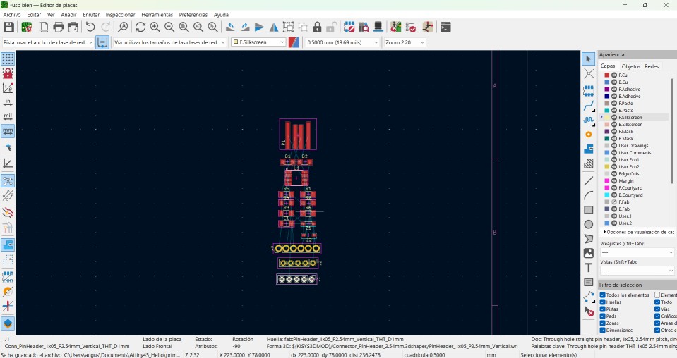
As you can see in the image above, all the components are too much together, so we have to move them in order to better accommodate them and thus shape the wiring that the components will have. Another thing I recommend you do is to remove the names of each component, as these are not so necessary for this process, since the entire circuit is marked with a gray line that appears next to each component. So to remove the names, on the right side of the program remove the option of front mounting fingerprints and proceed to accommodate the components in a way that do not collide with each other.
This is how I initially decided to put my components, but it is very likely that I will have to change them for accommodation topics.
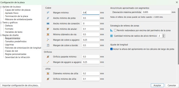
Now, it’s time to put the design rules we’re going to have to follow, these design rules were seen in week 4 "Electronics Production". To access the design rules we have to go to the file section and select the option of plate configuration, once in this option we go to the section of design rules and select requirements. The only things that are going to change in this section are: minimum track width and minimum margin. The minimum margin will be 0.4 mm and the minimum track width will be 0.5 mm, the rest of the data are correct, only these two are going to be modified. The following image shows the correct data.
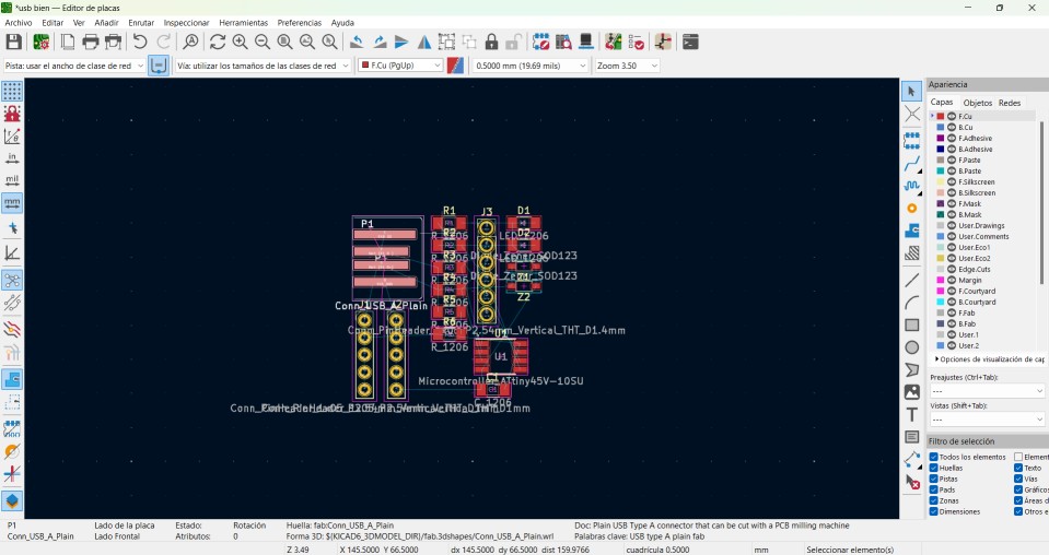
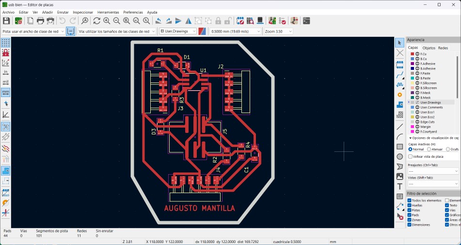
After about an hour and a half I managed to find the best accommodation for the circuit. Having arranged the circuit you have to start wiring it, the wiring is made according to the design rules we established before, the wiring tool is on the right side of the program in place number 4 represented as a broken line. The default program will try to connect everything regarding the schematic design, this is the result of my wiring.
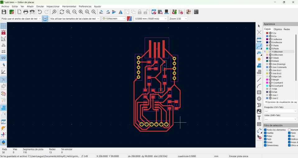
Since the wiring is done, it is necessary to make the part to be cut from the board, this part will measure 1 mm wide. In my case, I drew something like a USB.
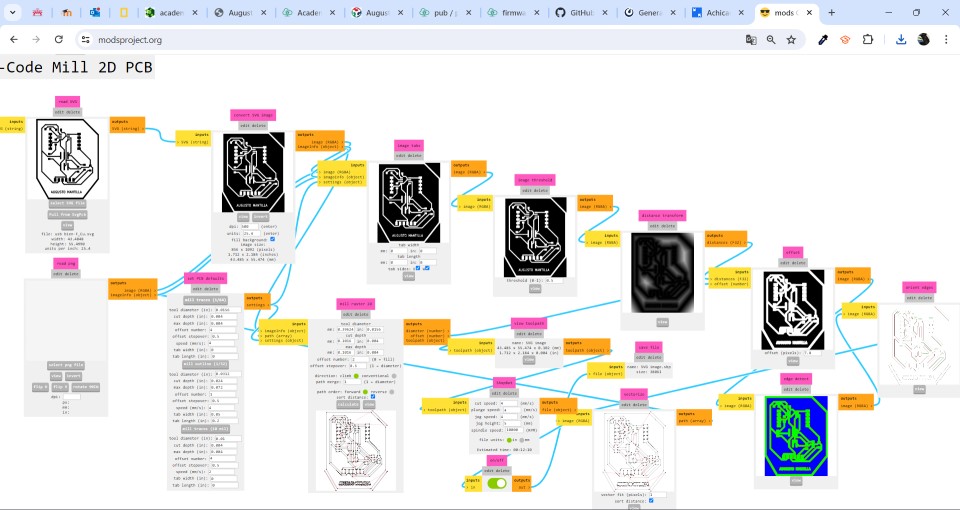
Finally we export the file in . SVG format to later use the Mods CE page, in this part I had many problems to be able to get my format in G code, for some strange reason I could not get the correct cutting strokes, so I had to occupy the format option. PNG, but this was not enough to get the right strokes and at the same time the format in G code. After being 2 hours with my advisor we were able to get the right strokes and the file in G code, this was achieved by putting both formats on . SVG and .PNG.
Due to time issues I can not use the Monofab SRM-20 milling machine so I had to use another milling machine from one of the Fab instructors, the disadvantage of this one is that I had to redo the file in G code, but on this occasion I had no problem as I already knew how to fix the problem that appeared to me when using Mods CE. These were the parameters.
.jpg)
.jpg)
.jpg)
.jpg)
.jpg)
Having already the G code, you have to open the Universal Gcode Sender program aka "UGS", I had to use this program as it can read the Gcode and translate it to the milling machine so that it can cut effectively.
After connecting the milling machine to the program we can add the Gcode where we have the strokes and cuts of the plate that we want to cut. Once you have uploaded the program you just have to place the tip in our origin where you will start cutting. Another important thing is to start cutting first the part strokes and at the end the part of the cut on the edges, this so that the plate does not move at the time of cutting, also before cutting check that the tip we are using is the right one and thus avoid inconvenience in the future.
This is the milling machine cutting
After the cut, the components have to be welded to the plate that we have just cut, the components are exactly the same as those in the schematic diagram, only this time they are in physical form.
Another problem I had was that the milling machine I used was not entirely accurate and it came to take a few pieces of tracks from the plate, it was not much but it would be complicated when soldering, this because of the lack of space.
At the time of soldering I had no problem, as I had previously soldered on a copper board with a soldering iron, there was a great improvement in my soldering technique compared to previous weeks. This is the final result after soldering all the components it required.
.jpg)
Files
KiCad
Re-Design
Due to programming problems and practicality I decided to redesign my board this week. The design I’m going to make is going to be one in which you will not have the design of the USB, but a simpler one. The following table has all the components that I'm going to use for the re-desing of the board.
| Qty | Component | Schematic image |
|---|---|---|
| 1 | Microcontroller ATtiny45V | |
| 1 | ISP | |
| 1 | Capacitator | |
| 2 | Led | |
| 2 | Power 5V | |
| 2 | Ground | |
| 4 | Resistor | |
| 16 | Pin | |
If you can notice, these are very small changes I made compared to the previous one, I only removed the USB footprint and 2 resistors. This will facilitate the soldering process. This is the schematic of the board.
Following with the steps I did for the last board, now I have to pass it to PCB Design, the design was as follows.
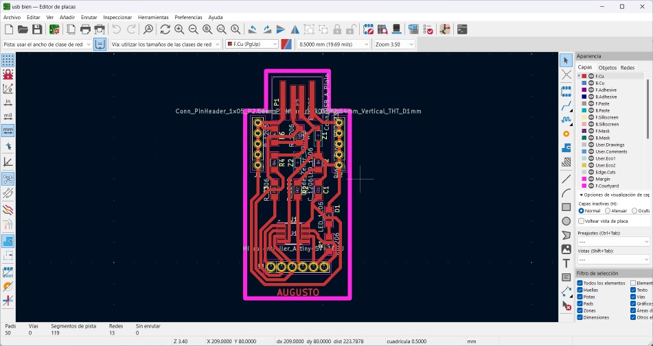
Note: One if my mistakes in the last board was put margin insted of a edge cut. So, in thid board I change that.
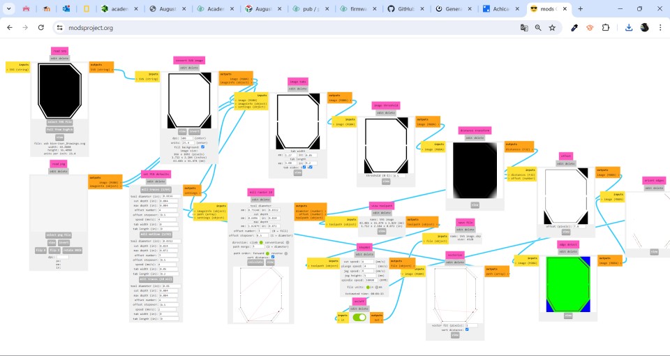
Saving the files in .SVG as I did in the past desing I need to go to Mods CE page to configurate the parameters for the milling machine that I'm going to use. This time, I could use the Roland SRM 20. The parameters were the same as the week4. If you want to know with more detail how the parameters are, click in here.
This is for the traces of the board
This is for the cut
Controling the milling machine
The configuration of the milling machine controls is the same in week 4, if you want to find more details about the process click here.
When connected to the milling machine, I sent the board traces first, so that it has more stability and does not move too much. After making the traces is important to cut the board.
This is the milling machine making the traces
This is the milling machine cutting
Soldering
Having already cut the board, I need to start soldering this board, for this is necessary to have already the components that I will occupy, in my case the components gave me fast so I did not have to wait long to start soldering.To start Soldering it is advisable to start with the smaller components, this so that it does not become complicated to solder them after. This is the final result of the soldering.
