Footprint libraries
add the fab.pretty
This week and the next are more learning weeks than machining weeks, all the theory needed to create something electronic based compiles in an extended series of documents, videos and the learnts from our tutors, putting some knowledge in practice i can use EDA tools, to design, preview, milling and solder to produce a board like in week 4.
I know 3 EDA tools, the first one would be Altium Designer, known for its powerful integration of PCB design, simulation and data management tools. Fusion EDA on the other hand offers a collaborative and cloud-based environment. KiCad an open source option, popular for its accessibility and robustness, with many functionalities for PCB design without the costs associated with commercial tools, I consider kicad to be at least at the level of Fusion EDA so I will use KiCad, Download KiCad
I want to test the attiny 44, after reading the specs, that microcontroller offers good settings enough to test the outputs and inputs in future weeks.
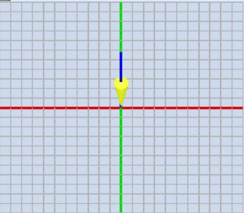
This week Group assignment, It consisted of learning to use tools to measure and test our electronic projects, you can feel confident that your project works by using a multimeter to check each path and connection, checking that the values of resistors, capacitors, diodes are correct and measuring that the power supply is adequate, however to check if the communication, if your program works as you think it should and if the electronic devices work you need an oscilloscope,It allows you to view and analyze electrical signals in real time, making it easier to detect anomalies such as noise or unexpected spikes. This tool offers accurate measurements of voltage, frequency, and phase. It is also essential for verifying the integrity of signals, especially in high-speed circuits, ensuring that there is no crosstalk or distortion that could compromise the performance of the design.
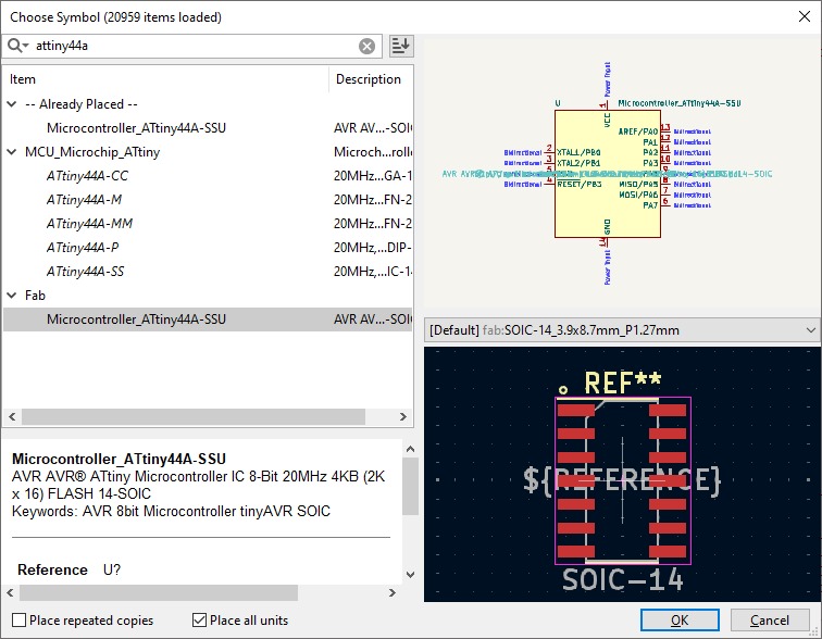
You can work directly with the components the basic KiCad brings but, the correct way to work is to use the exact foothprint you are going to use for Fabacademy there's a folder with the components,download.
The first time you set the next parameters some warnings will show up, just accept and complete the changes, to add the libraries click in the plus button.
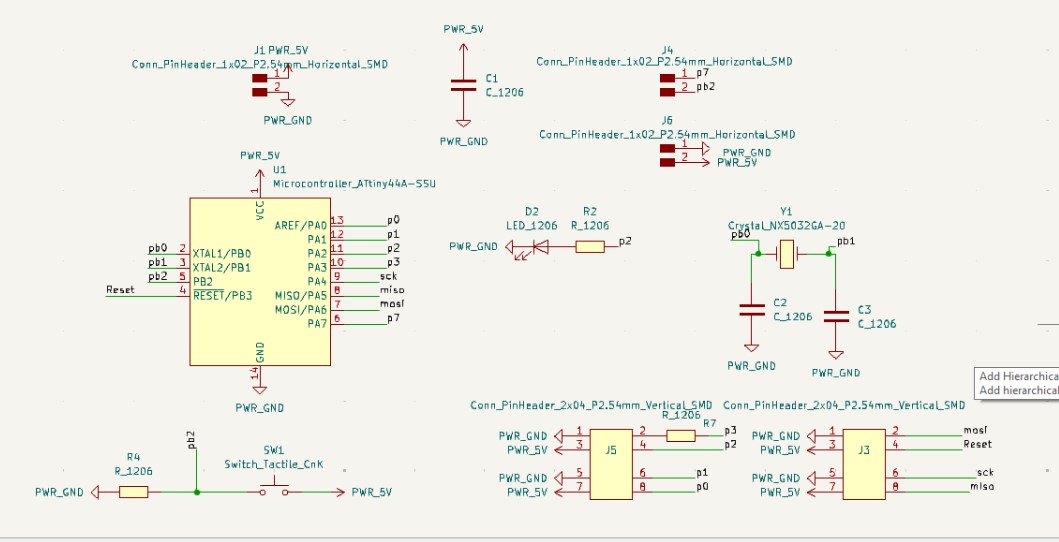
Now you can start creating a new project, and then click in the schematic, this is the first step that works as a layout of the components you will need and the connections between them, i will breafly explain the tools i'd used.

In the image of the right you can see, if you uploaded the libraries right, the components the fablab should have using the fab tag and the Name of the component, when you selected a little spreadsheet behind will show aswell as the connections module for the schematic and the print in the PCB.
The arrow tool let you choose and drag the components frequently to join them instead of wiring. The third tool is the one for including components, it opens a tab where you can find the components easylly using the fab tag in the search space. The fourth is the ground and power components very usefull. Then the tools with an A helps you create connections between components, we aren't doing the cable managment section here, so use those tools and link the components with text tags for each pin.
There are lot of things to have in consideration when designing PCBs:
The components i used:
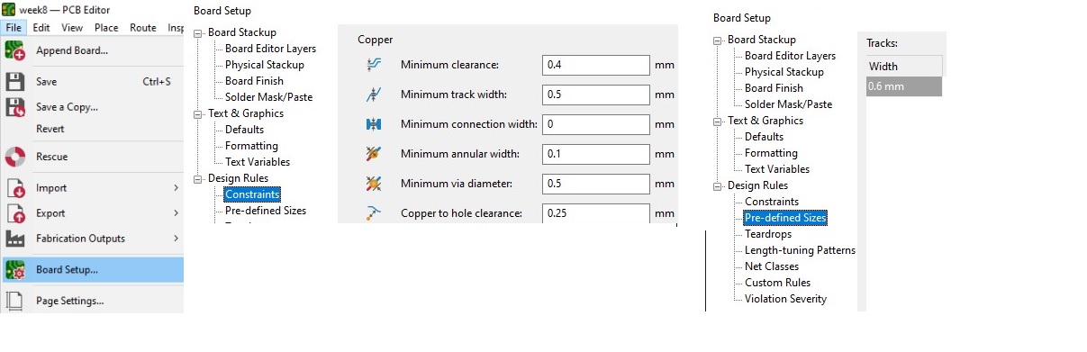
Before starting with the design and position of the components and paths we have to go through the design rules, these are defined by two issues: the size of your tool and the amount of current that will pass through the path, to know the necessary width there are many web tools, you normally make 0.5mm width at least to make the soldering easier, depending on the tool normally 0.4mm width is the minimum clearance you need to specify, when you are designing and when finished your design you can run a safety check that will mark if this are violated.
On the top of the image you can see 4 buttons, just the first two matter, the first one gives you the components in the schematic, and the second one shows an analysis of issues tab, once you finished always check.
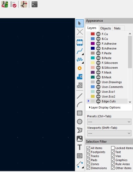
In the column there are other tools like the draw figure to draw the edge-cuts and other things, the T tool to add text and the others dedicated to style the traces.
Finally in the right there's also the appearance tab where you can show or hide layers, also, you can select the one to edit or draw there, this is usefull when working with multiple layers PCB in our case we are just using the F.Cu layer.
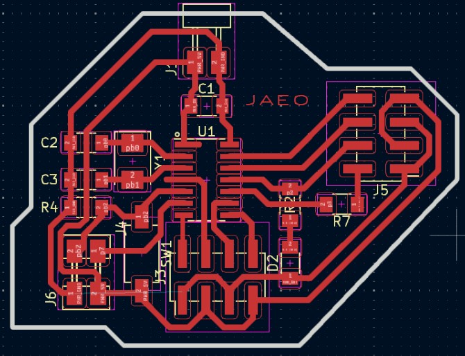
Make the layout for the components, join them with diferent traces and the needed trace width pressing x to activate the trace creator; for example the Attiny44a-ssu trace width is about 0.6mm so i made horizontal traces to make the soldering easy, then add a margin with the draw figure tool to create the border with the width of your milling tool to cut the PCB, then export the files of F.Cu and the border files, if you export them as svg. you will need to add an invert to the steps shown in Week 4.
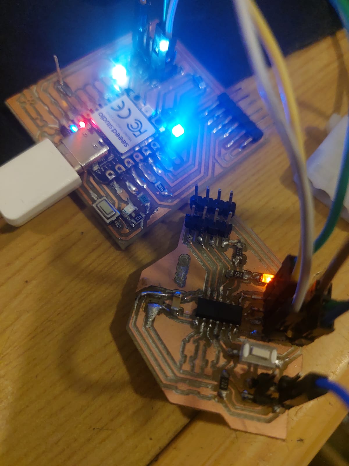
The last thing would be to calculate the necessary resistance for the diodes, in the datasheet of the orange diode it says it requires 2V of direct voltage and 20mA of direct current, so using Ohm's law as in the image I show R = V/I.
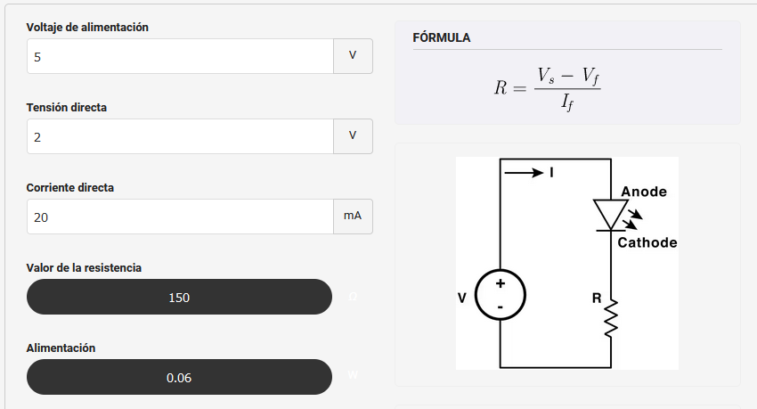
To check the value of the voltage you would need with a multimeter to place the black tip in any ground trace of your circuit, and take measurements: one before de resistor of 5V, another after the resistor around 2V more or less and another after the diode close to cero, the idea is that each component consumes some of the voltaje the microcontroller is sending, while the current is determined by the needs of the diode in this example.
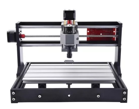
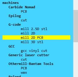
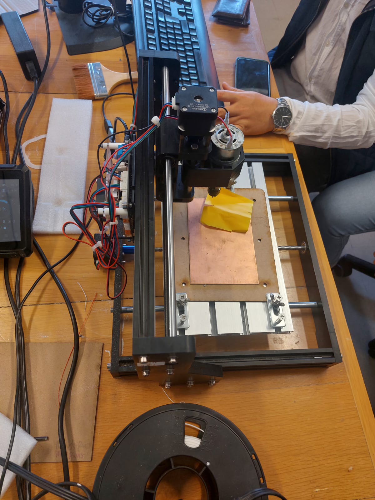
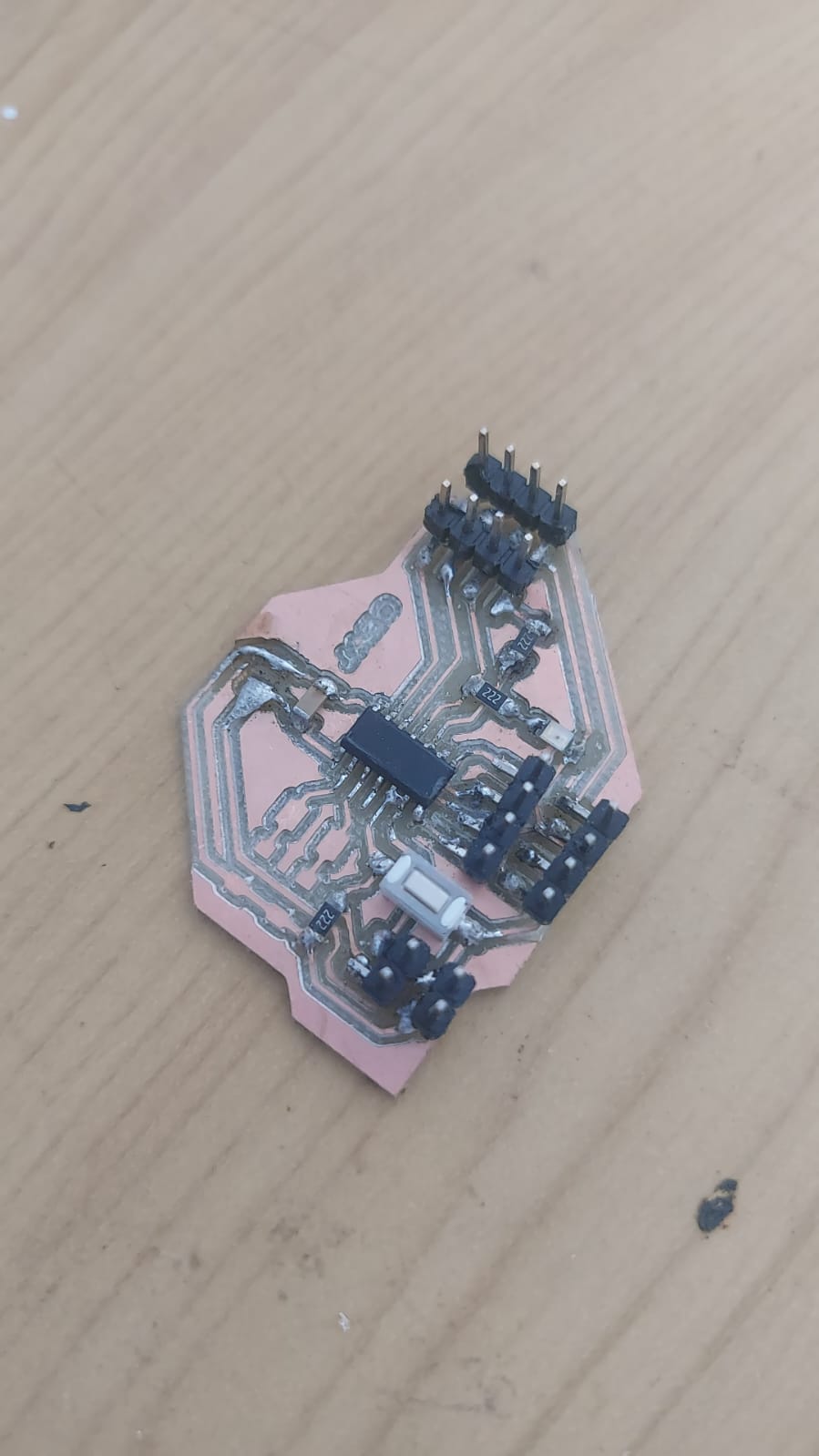
I made two PCB just for the experience of using a different milling machine, we have like 4 hand crafted models diy, and i wanted to test them to realize the quality of the roland, yeap, now i see the improvement, the process is pretty similar to the one with the Roland with some changes: first in mods you select a generic machine for milling 2D PCBs, then since the machine doesn't come with a licensed software you will need to use Universal G-code sender, again all the same steps of setting zero axes and the main problem, is that the traces sometimes appear allgin to cero without leaving margin for the edge cuts, that was an issue too.
To create one usefull PCB i finished one "copper" plate, fighting with the depth of the traces, the machine decided to vibrate and other errors made me really a lot of headaches, in that last attempt the power pins and many traces took off, i decided to stop testing and made a new one in the rolland which gave me a little challenge making the traces like 0.4 mm. In the process of desoldering and soldering again the attiny got cooked, something i didn't realize until many hours later.
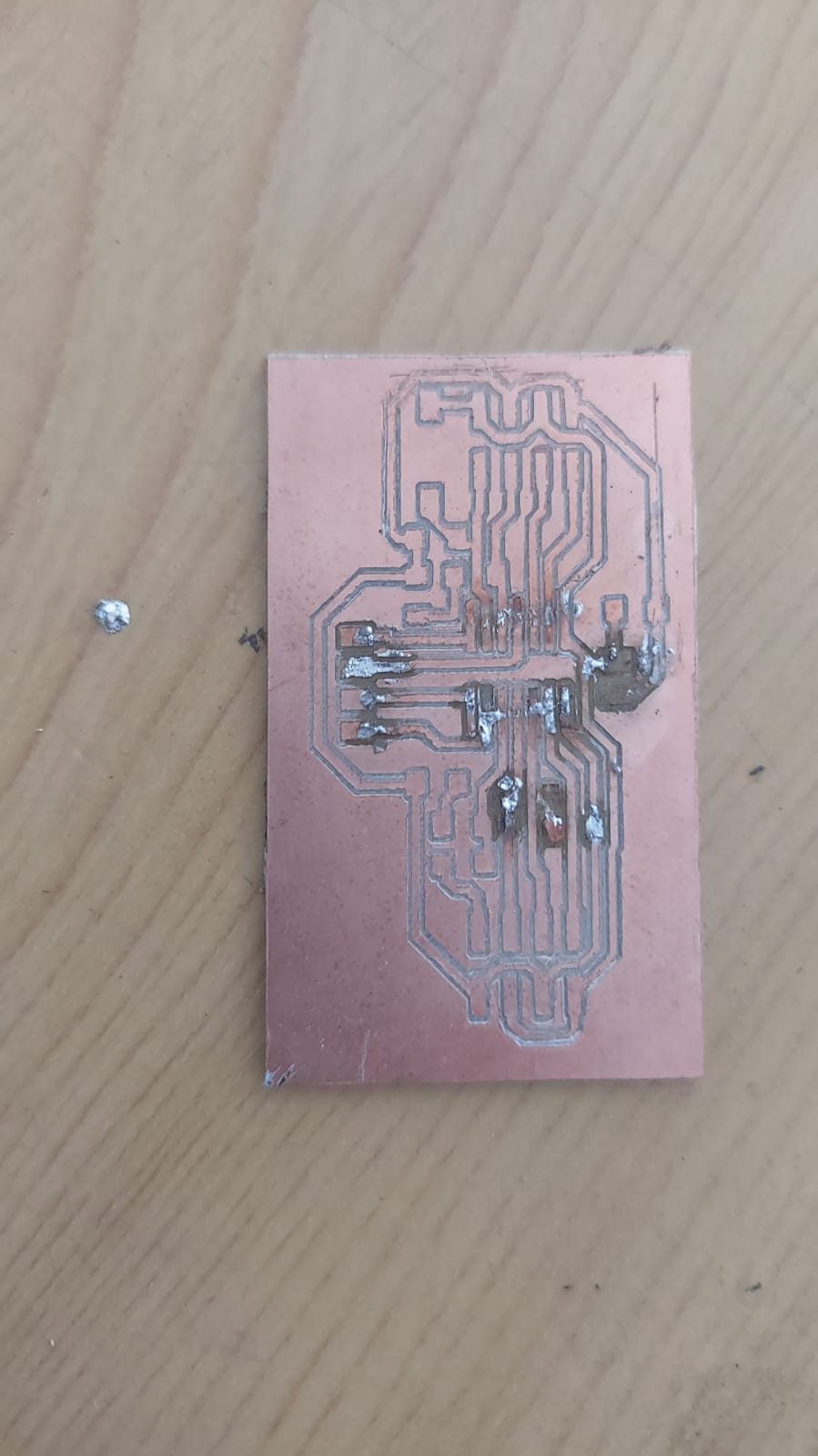
With a new microcontroller after the semana santa hollidays i programmed it following the steps in the quentorres page, for the next PCB i should be extremely cautious when soldering the power pins again ];
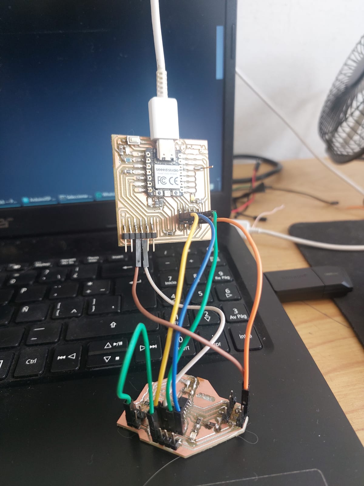
Download the Schematic and PCB design with extra room, for an easy soldering: KiCad.zip.
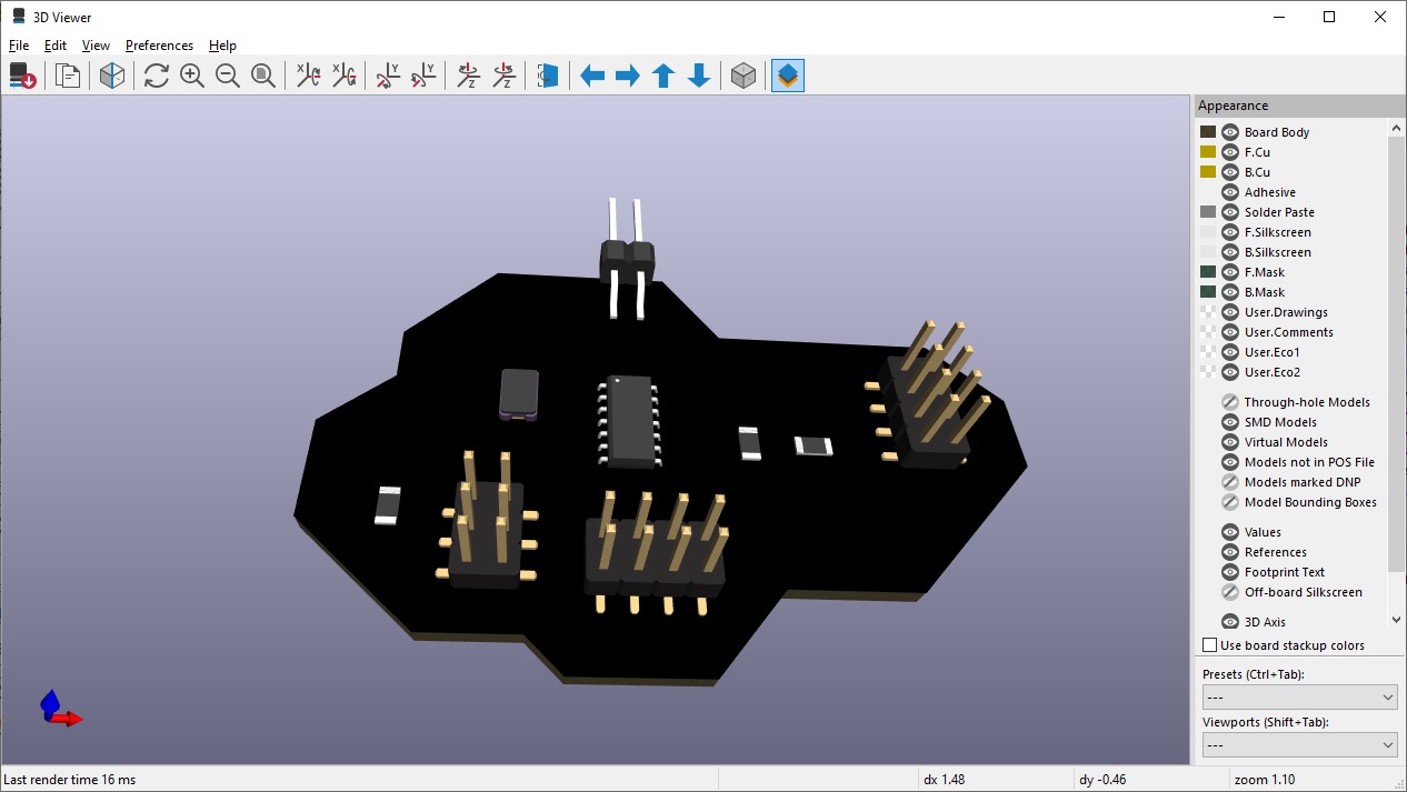
I don't know why the capacitors, led and button aren't showing but here is the 3D model.
Throughout the week, I faced technical challenges that required a solid understanding of electrical principles and the small components needed to create a PCB. Using advanced EDA tools like KiCad made it easier for me to create accurate and efficient designs. Additionally, learning how to use an oscilloscope to verify and debug my design gave me a practical perspective on how theoretical design principles translate into the real world. Designing and producing the same board but with improvements helped me identify things that aren't taught like the position of components so that when soldering, components or even the tracks themselves don't come loose.