4. Electronics production
In week number four, the main theme is learning the bases of electronics. To achieve this, in the group assignment, we will discover the making of a custom PCB and then send a batch across the sea to a cheap Chinese manufacturer where they'll give the PCB the usual colours 'protections'. Is my job to make a predefined PCB in the milling machine, solder the components and run a test software.
The group Assignment
Brief summary:
The instructors will give us the fabric parameters of the milling machine, explain the steps to use it, describe the different tools used in the milling process, specifically the tips used for engraving and cutting. Explain the controllable parameters: drill hole size, material to work with, number of layers, the minimum clearence and width; how to convert the files to .rml (the type that monofab supports); using the page mods, at last see the results of different combinations of parameters in the milling file. Link to the: group assignment
-
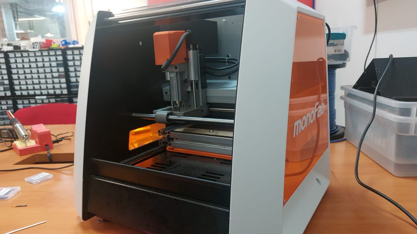
The Milling machine
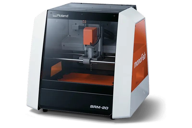
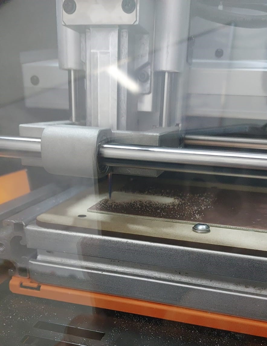
The machine we will use for this assigment is the ROLAND SRM-20, the way this compact tool works assembles the traditional drill, but in miniature, it can cut: Modeling Wax, Chemical Wood, Foam, Circuits, Acrylic, Polyacetal and Acrylonitrile Butadiene Styrene (ABS), with the dimensions of: 203.2 mm (X) × 152.4 mm (Y) × 60.5 mm (Z),
-
Like in the laser-cutter machine in the previous week, we'll have to adjust: the coordinates, Drill hole size (dependant to the tip and settings), the choosen material, Minimum clearence and Trace width and last but not least the number of layers (laps).
-
-
-
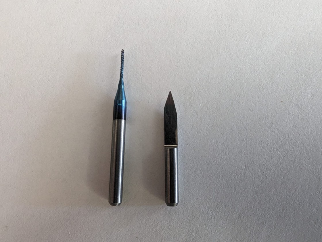
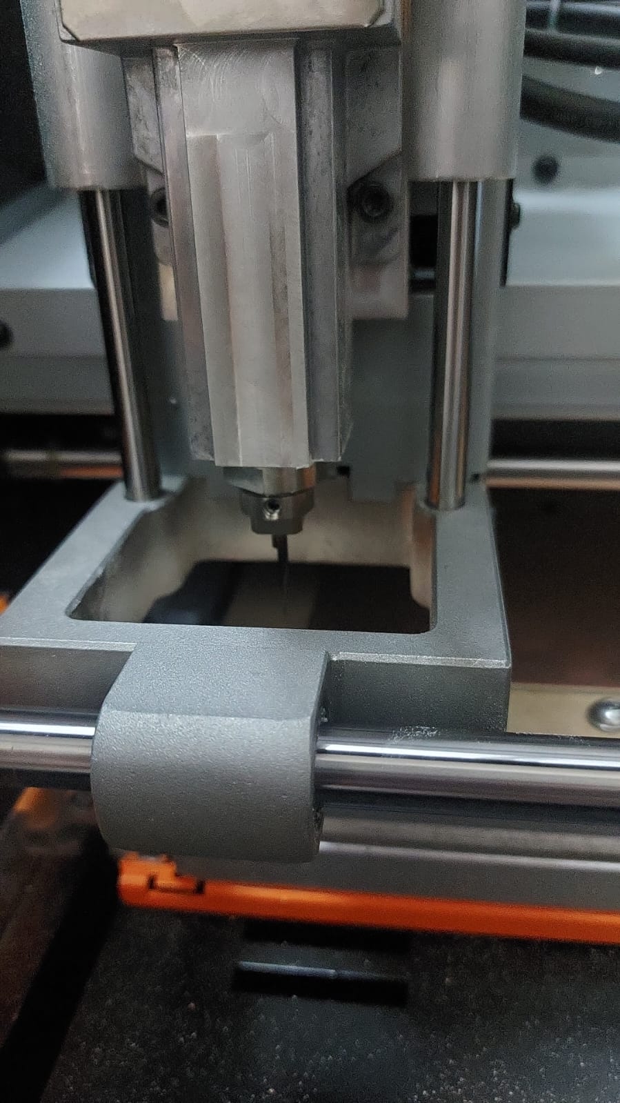
There are two principal tips we are going to use For engraving we're using a 15 degree V-bit, for cutting we're using a 0.8 mm diameter two flute end Mill.
The tips we use and the own machine parameters make a complex array of possibilities, fortunately already exist a tool especiallized in giving the milling machine the correct instructions, yes i'm talking about mods, this website works as a settings panel for our machine and similar ones, with the help of different modules you change the .png files to .png.rml .
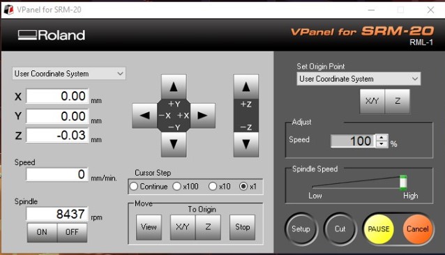
Also the software needed to controll this specific machine: link to the drivers needed and the Vpanel for the visual settings needed.
Personal Job
In this task I need to make my own PCB and then solder the electronic components, more specifically Surface-mount technology (SMT), it's a hard task even if you have experience, so what you should do is keep practicing!, once the introduction is finished lets continue with this week's machine diagram:
Steps to make a PCB
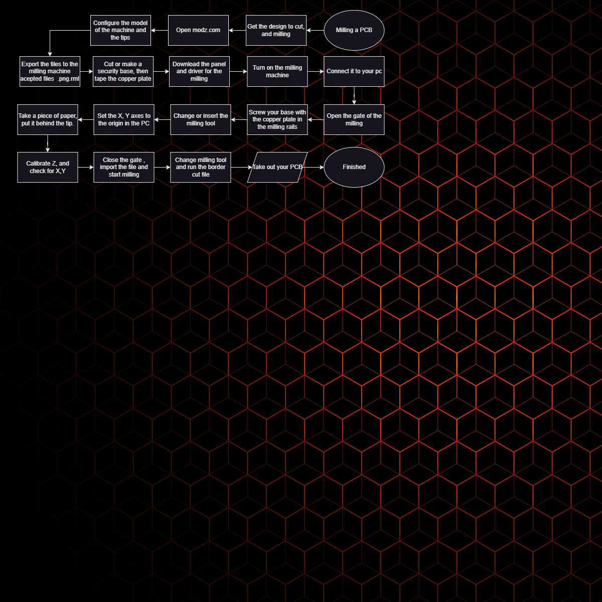
Getting Ready
-
In order to start making our PCB we shall make a support for the copper plate to prevent damaging the machine in an unfortunate coincidence, Uber instructor sent us the next file: bed for the milling machine, then we cut it in the laser-cutter using MDF.
-
The material all have used is FR-1 one of the most common in PCB making, the advantages it gives are: fast working, prevent electric fails while soldering and is easy to keep clean.
-
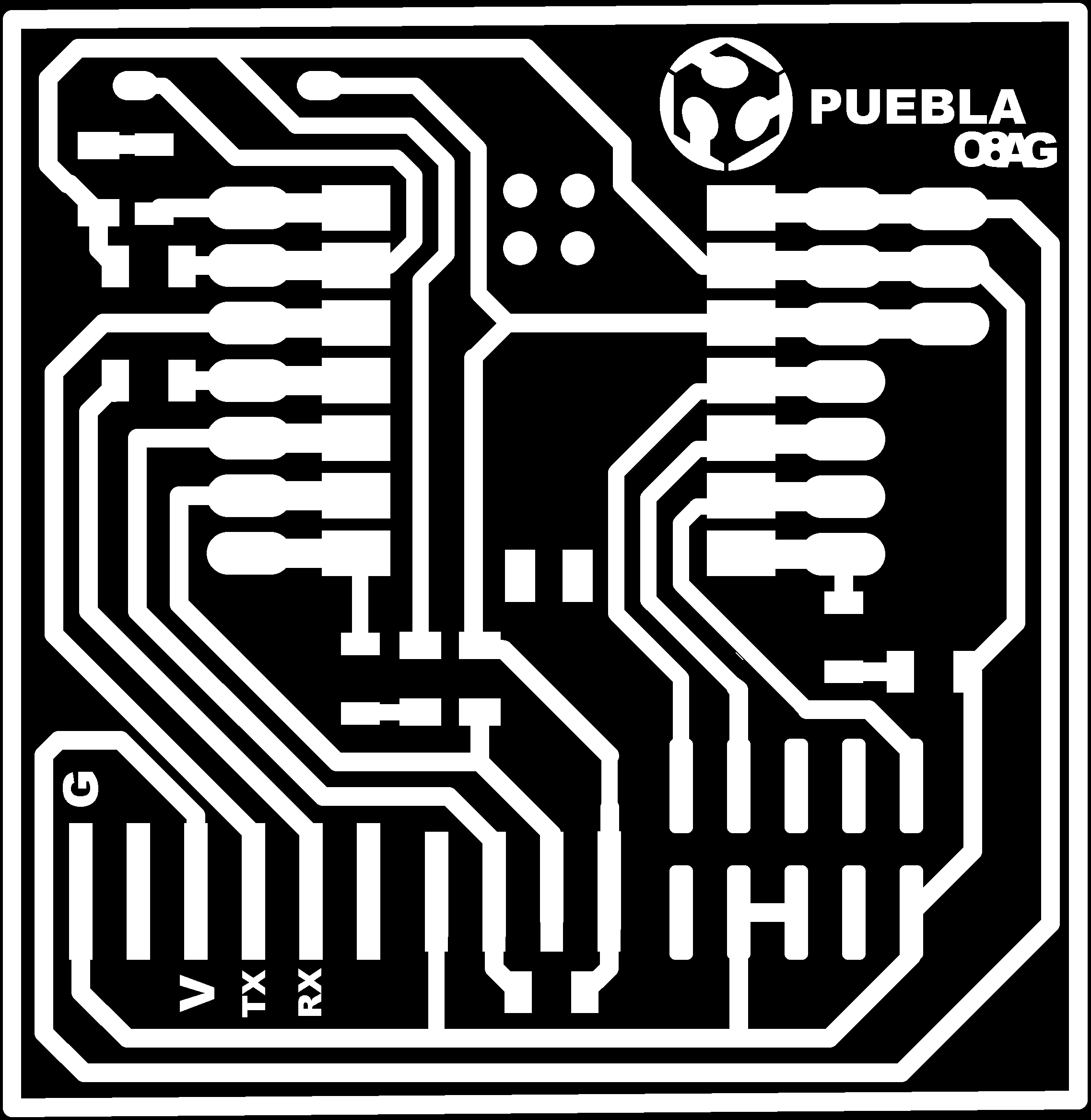
The design we are going to make was made by our instructor O8AG, he gave us the next 2 pngs: The paths and The border cut.
Mods
-
When you enter the page richt click, then programs/open programs and go the specific machine and method, in this case mill 2D PCB, the in the left side a little down you will find the select png file, first the one with the paths, following with the set origin to 0's, then you can change the tool diameter and the offset number, you can left the tool diameter as it's stated (in mi case I putted it in .8) and the number in 2, after that turn on the right button and click in calculate, the program will download the file and give you a preview.
-
For the border file set the pcb default to mill outline and repeat the process but when you have imported the png, invert it so it does what is was intended, obviously dont change the raster 2D parameters if you set it to outline in the past instruction.
Now we can go to the monoFab, connect it to your pc with the programs downloaded, turn it on, screw your bed, open the virtual panel set the origin there for the three coordinates, the technique used here was to place a post-it below the tip, when it is un-moveable, remove it and lower a .01 mm more, the turn it on and lower it a little more.
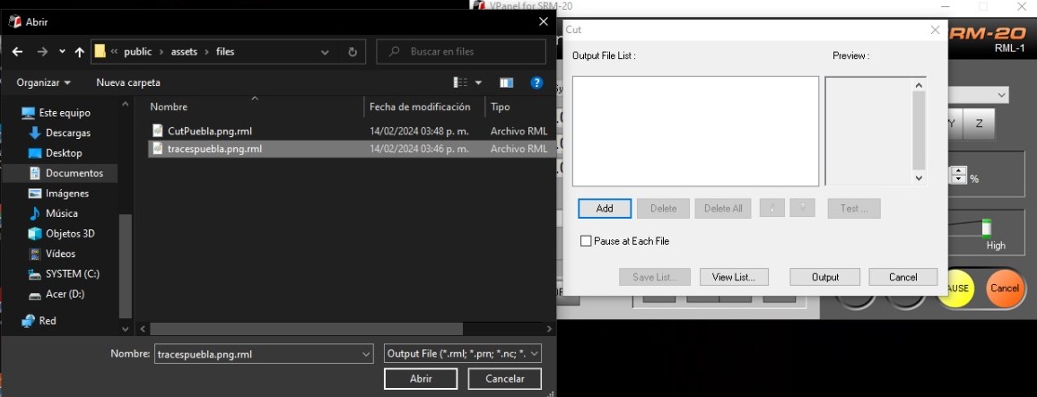
Click in the setup button amd import(ADD) the first file, get this machine working!.
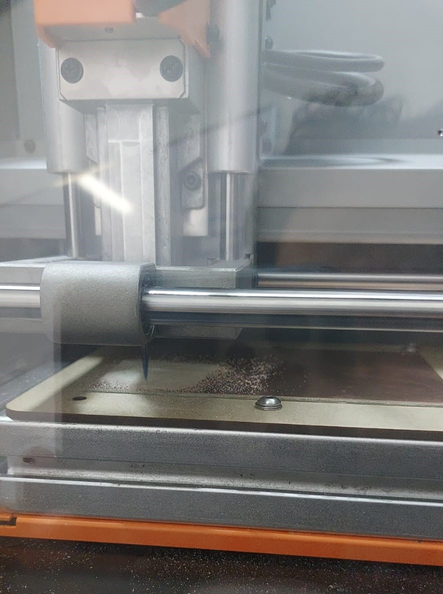
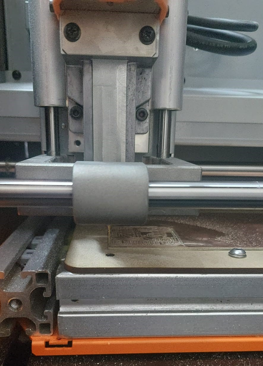
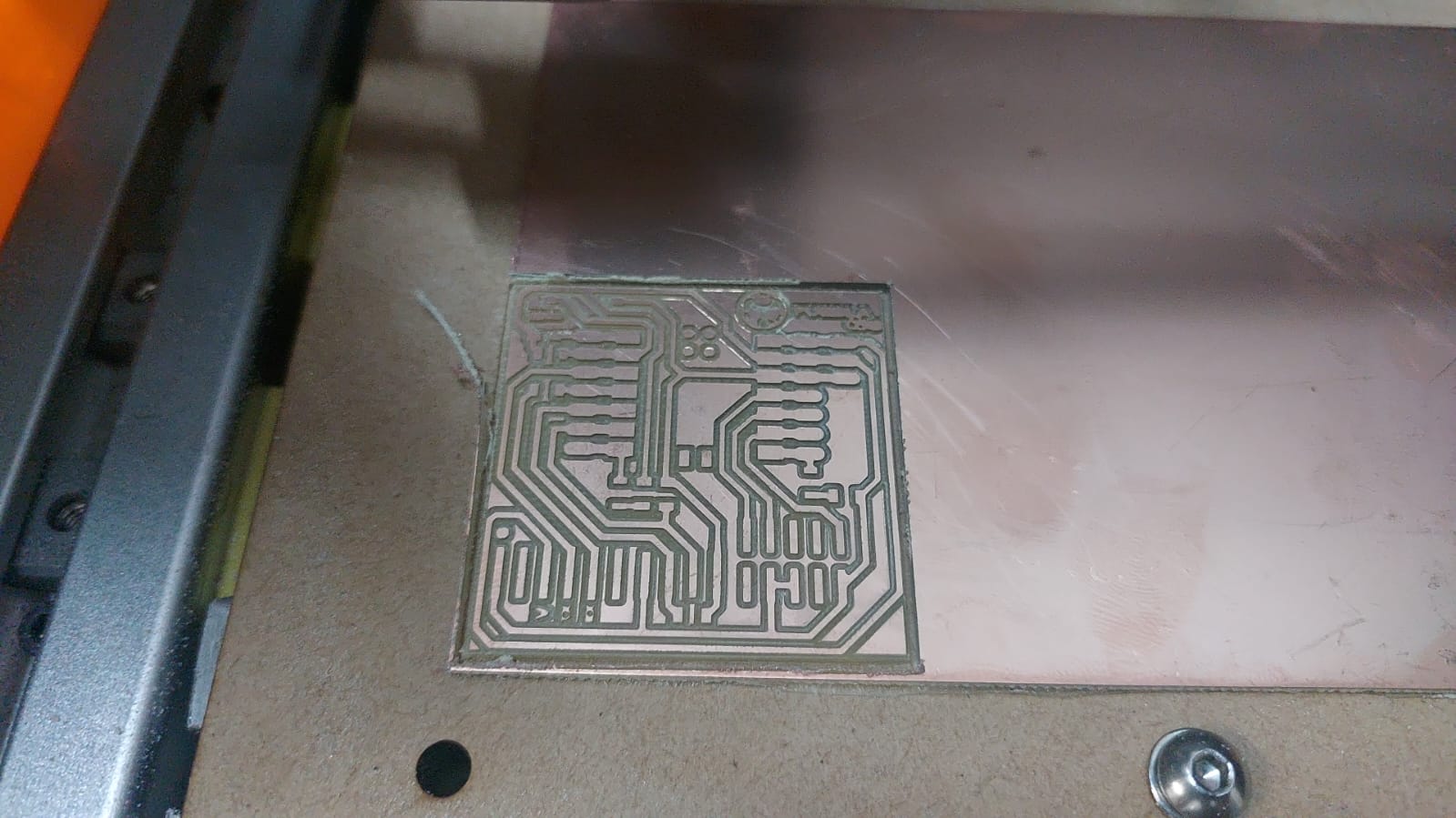
In the last image you can see my PCB almost done, but 2 things had happened, maybe because i shouldn't put the width of my tool in 0.8 there was a big part that doesn't touch, probably because of the system inferring that it wouldn't be able to, or it doesn't make it because the tip wasn't screwed at all initially, when the process finished the tip falled instantly.
I vacuumed and decided to run the program again with those two things fixed, the width of the tip now set in mods To the original 0.39mm.
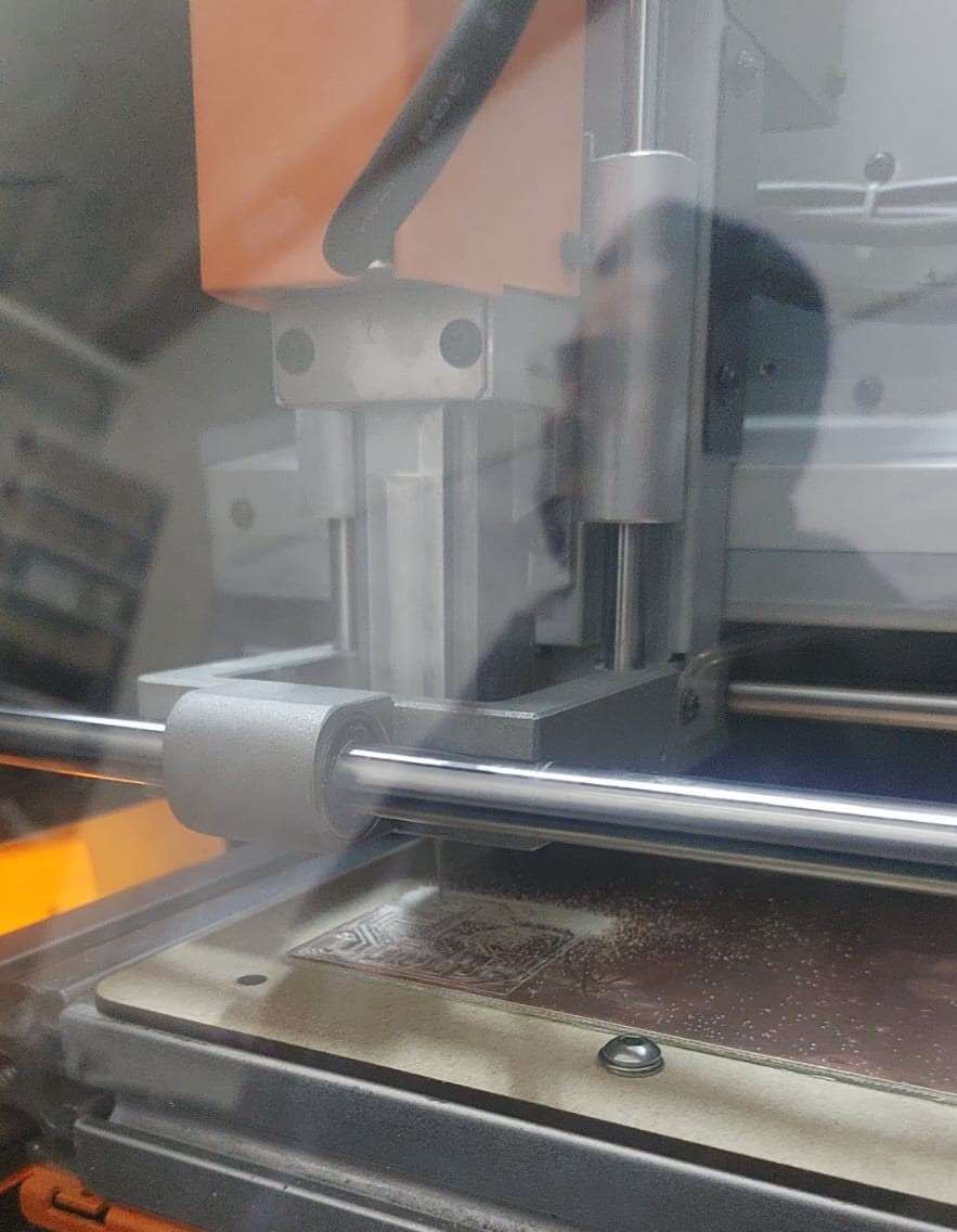
The final result is pretty good, it leaved wide enough paths, the margins we expected and a good result in sight.
Getting Ready TO SOLDER
Along with the design for the PCB O8AG gave us the map of where the electronics go and the typical electicity diagram, where you can understand the matter of the resistors, capacitors, transistors, etc.
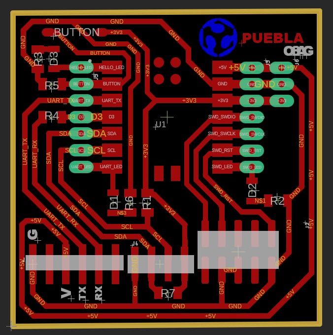
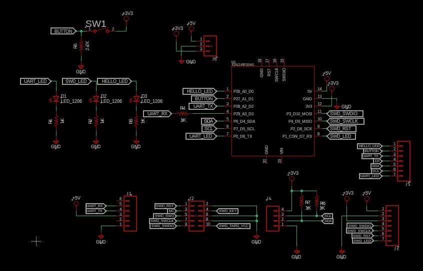
The electronic components used are: The arduino based Seeed Studio Seeeduino XIAO 102010328, 3 extra leds, 5 1k ohms resistors, 1 2k ohms resistor, a push button and enough pins to plug external components when the embed programming week comes.
-
-
The technic i've used to solder was to add the less amount of thin i can in one of the sides of the component, put it in with the head to try fixing it, add more tin to that side, then in the other side and check.
-
I wanted to solder in a quiet place, which meant Iberofab wasn't the best option. I thought there would have been no problem soldering in my house, but I ran out of luck.
Just the week i needed the equipment my father decided to take it away, so i had to improvise, i got an old magnifying glass, 20 years old tin and soldering paste from mi father university undergraduate and my moms remove hair clip.
Started soldering the little components and the pins that just needed a little tweak, then the rest of the pins bended at 90 degrees manually and finally the Seed Studio Xiao after i used some black insulation tape in it's back.
1mm from goal
-
-
Where you see the usb logo click, then select other boards and search for Raspberry Pi Pico and select that, it's Also recommended to choose port 3 or 4 if it's not auto selected.
Then in the same place now you can choose the XIAO-RP2040, to run the code you can open paste it or when openning this file: Blink opens the arduino app directly, it will say the file needs to be in a special folder, say yes to all.
The code makes two leds Blink and the third one needs the button to be pushed in order to blind.
-
The only thing that remains is the basic programming to check if all the components are well soldered, it's good to know that i checked all the connections in my path using a multimeter to check continuity and resistance, to learn how to program the basics here is the official wiki.
It will ask you to download the arduino controller software.
To start booting the Xiao, before you connect it to your pc, push the boot button.
Then in the software to go to File tab/ Preferences/ aditional boards and paste this reference: https://github.com/earlephilhower/arduino-pico/releases/download/global/package_rp2040_index.json then download it.
A really fun and mechanical focused week where a little miscalculation could destroy all your progress, as one of the videos of surviving fab-academy said: dont drink coffee when you solder, i make the comparission with and without and all i can say is that the day i drinked i burn myself.
Final reflection
the PCB manufacturing process requires bringing the milling tool as close as possible, if necessary lower it further and make a small hole, otherwise there are paths that are not only difficult to correct but also generate errors and if the paths are not deep enough when soldering the copper layer can come off, having to re-do the board in extreme circumstances, soldering is a process that every time you solder a part and look at the inside you realise how bad it was and so on to infinity where you cannot perceive it, a long road.