Designing my own PCB!
Couldn't have nailed this assignment without Erik Gonzalez, another student at Fab Academy. Big thanks to him! He showed me the ropes on what components were needed to put together a neopixel matrix that looks like constellations. My goal was to get the hang of programming neopixels for my final project and figure out how all those bits in a PCB work together.
My teachers also gave an introductory class in which they explained to us how to use a multimeter and the basics of designing PCBs, you can find more detailed information in group´s assigment page.
Choosing the right components
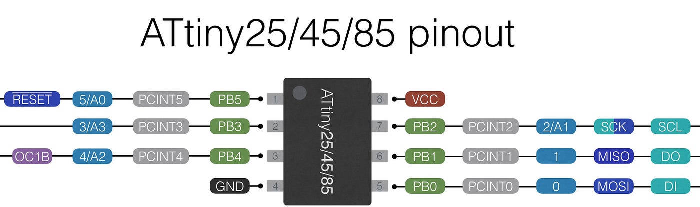
I went with the Attiny 45 microchip because it’s both versatile and straightforward to program, making it a great fit for what I needed to accomplish in this week’s assignment. Resistors are crucial in keeping the circuit’s voltages in check, ensuring we don’t fry the LEDs. I picked a 10k Ohm resistor for the connection between the 5 Volts and Reset, and a 2200 Ohm resistor for the link between power and ground. A capacitor is necessary to keep the power supply estable, preventing any significant fluctuations that could impact the circuit. I chose a 1 MF capacitor for its ability to ensure a consistent energy flow. For the project's light display, I used a ws2812 Neopixel, perfect for creating a constellation matrix. A button was also included to enable resetting of the PCB easily. Pins are essential for connecting the Attiny 45 to other elements on the PCB and facilitating the addition of an external LED strip, as well as hooking up other external devices. Sketching PCB Components Before moving to PCB design software, I sketched everything out on Procreate. This helped me visualize the connections between components clearly. I made notes on why each connection was made, aiding my understanding of the design process and serving as a handy reference.
Components
- Attiny 45 Microchip (1)
- 10 k Ohms Resistor (1)
- 2200 Ohms Resistor (1)
- 1 Mf Capacitor (1)
- 1206 Button (1)
- Neopixel Ws 2812 (11)
- Male Pins (14)
Designing my PCB
Once I had choosen the components I decided to sketch how the connections on the PCB would look. For this first sketch I used Procreate. For easier visual understanding, I color coded the different connections and wrote the why behind each one of them so that I could fully understand how I made the connections.
USING Kicad
First, before sketching I had to download the software and added the fab libraries. I'll leave the step by step guide to do this.
| Step | Photo | Description |
|---|---|---|
| 1. | Downloaded Kicad from link | |
| 2. | Downloaded the Zip file from gitlab | |
| 3. | 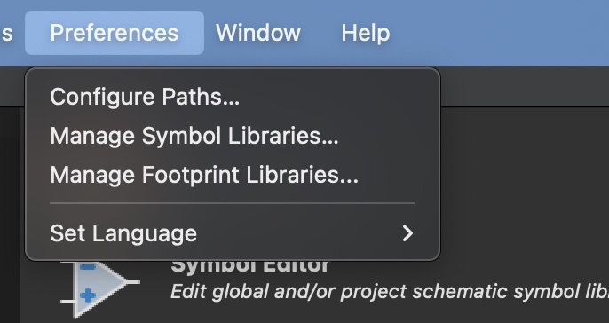 |
I had to integrate the libraries into Kicad, for which I selected the “preference” feature on the menu bar and then 'Configure Paths'. |
| 4. | 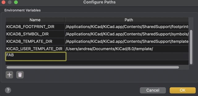 |
Added a new path labeled 'FAB' and inserted the 'fab.3dsource' folder. |
| 5. | |
Proceed to select the 'Manage Symbol Libraries' on the menu bar. Same as before, created a new 'Library Path' called 'FAB' and inserted the 'fab.kicad_sym' file. |
| 6. | 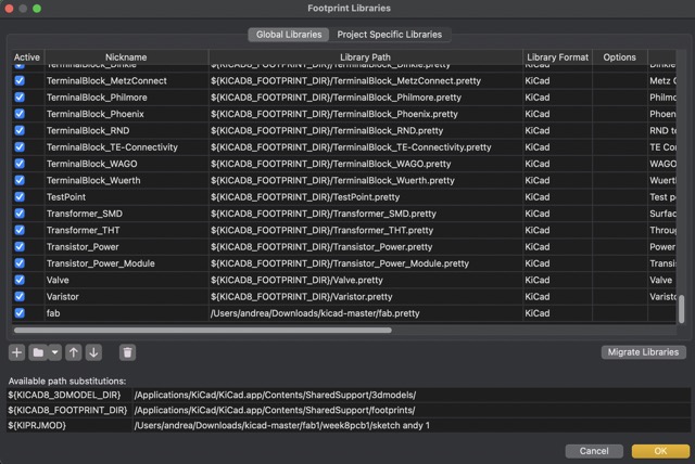 |
Finally, in 'Manage Footprint Libraries' on the menu bar, created a new path titled 'fab' and included the 'fab.pretty' folder. |
What is Kicad
KiCad is an open-source software suite used for electronic design automation (EDA). It allows users to create schematics and design printed circuit boards (PCBs). KiCad includes a schematic editor, a PCB layout editor, a 3D viewer, and various tools for managing libraries of components and footprints. It is widely used by hobbyists, educators, and professionals for designing complex electronic circuits and creating PCB layouts, thanks to its comprehensive feature set and flexibility. KiCad is available for multiple platforms, including Windows, macOS, and Linux.
COmparing EDA softwares I have used
I've also used EasyEDA, which is great because it's available online. While both EasyEDA and KiCad are similar, they can serve different purposes. I found KiCad easier to use for this assignment because our teacher provided us with a library of component footprints, making it quicker to work with the school's components. However, I used EasyEDA for designing my final project's PCB because I bought the components from an electronics store, and it was easier to find their footprints online. If I had to choose between these two software in the future, I think I'd prefer EasyEDA, but it was valuable to gain experience with both.
Schematic editor in Kicad
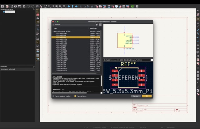
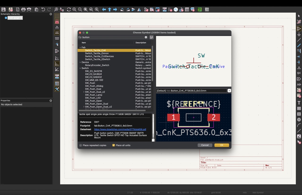
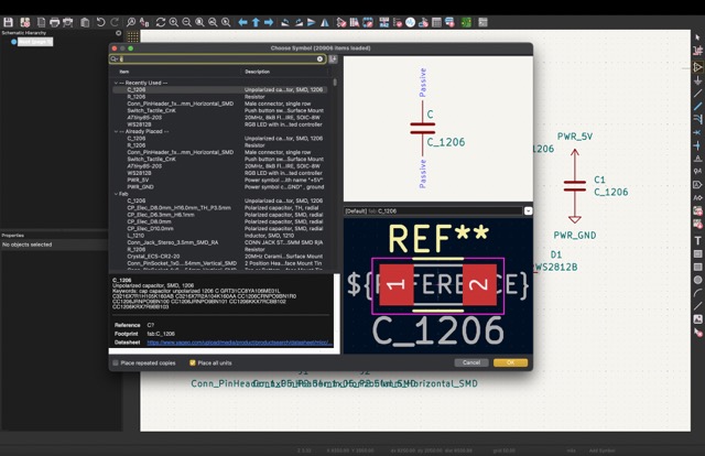
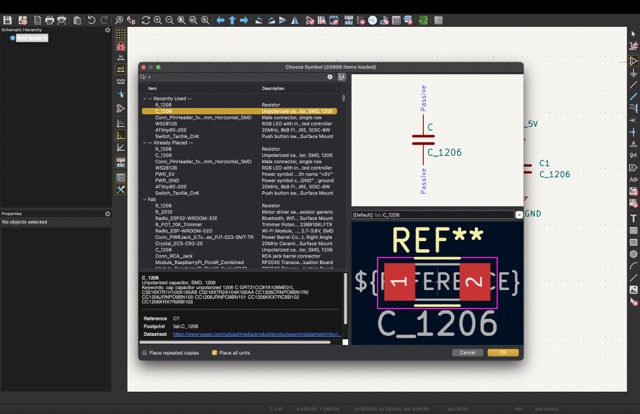
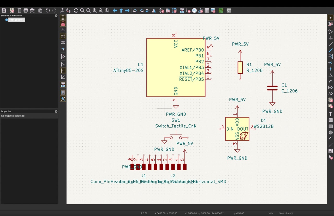
First, I selected the components I was going to use by clicking the “Add symbols” sign, and continued to look for the different components inside the Fab folder. I started by the Attiny 45, then the resistors and capacitor, the pins, the button and finally the neopixels.
Tools Used for this step
- Add symbols: to add new components such as microcontrollers, resistors, capacitors, among others.
- Add Power Symbols: to add voltage and ground to each component as needed. It is important to connect each component to ground and voltage since it will create the paths that will be used later to connect all the components in the PCB.
- Add a wire: or you can use the shortcut “x” to create connections between components.


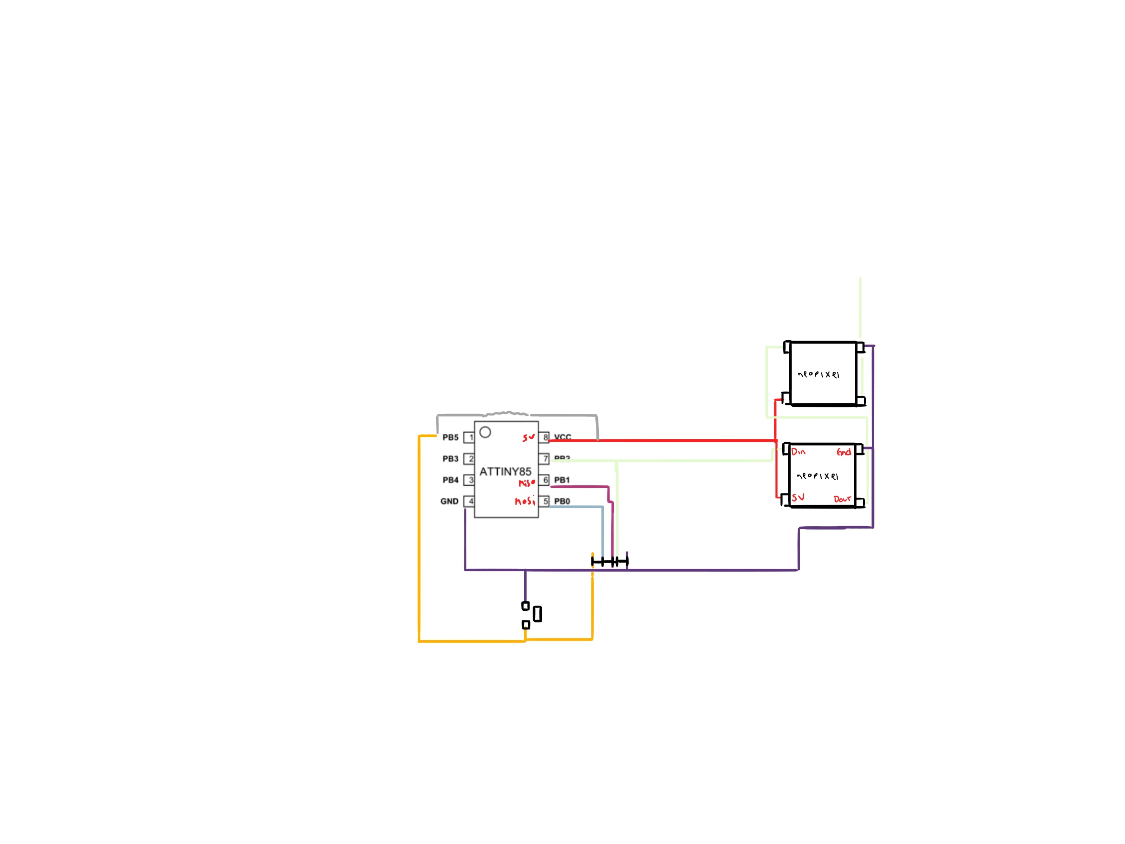
I followed the next photo
- I added the Attiny 45 and connected it to 5 volts and ground.
- I connected one resistor to the reset pin on the Attiny and to voltage. From the same “Reset” pin the button was connected, as well as to the ground.
- The capacitor was left alone and connected to voltage and ground.
- The second resistor I connected it to voltage, then to the led and finally the led to ground because it needed to create a closed circuit.
- The first 6 pins were conected to voltage and ground and then to the other 3 pins on the microchip. These pins were Reset, SCK, MOSI and MISO.
- The second pins were connected to voltage, ground and pin 7 on the Microchip since it is Din.
- The neopixels needed to be connected each to voltage and ground. Only the first neopixel on the circuit had to be connected to Data. All the neopixels are connected between each other by DIN and DOUT.
PCB editor
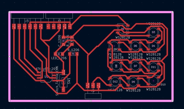
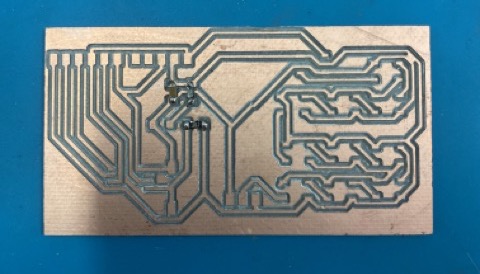
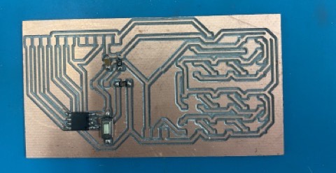
Once the sketch was done I selected the " Open PCB in board editor" on the top menu bar to create the tracks. Then I selected on the "tools" feature on the main menu and clicked on "Update PCB from schematic" so that the sketch that I had already done can be imported into the editor.
Once it was imported, I proceeded to arrenge the different components and created the tracks by using the "x" shortcut. The objective was to create the tracks without them interfearing with others. This was quite challenging.
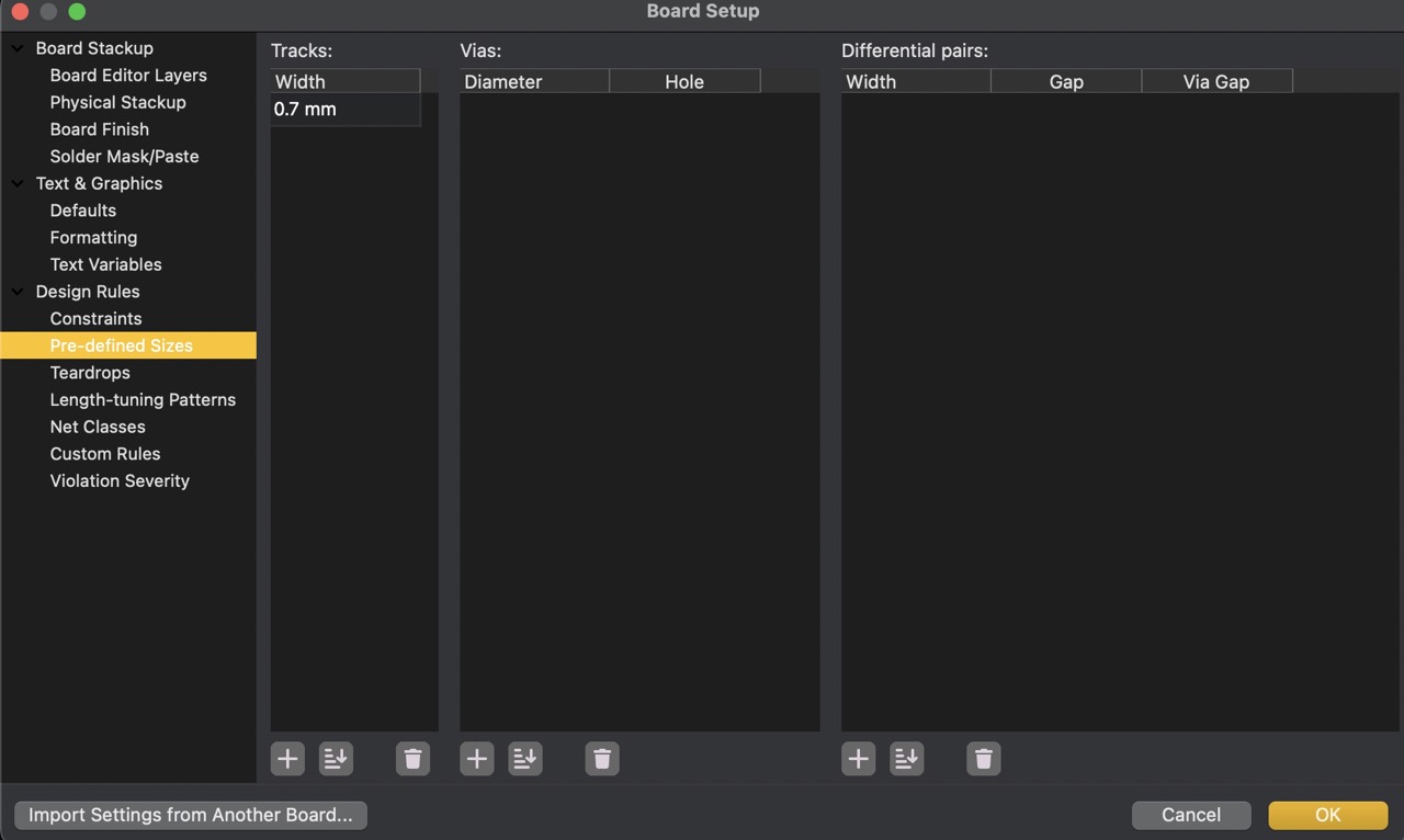
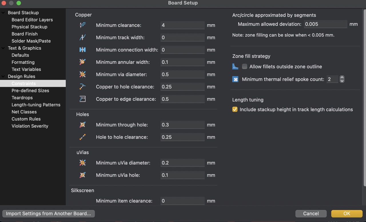
In the 'File' drop-down menu, I selected ‘Board Setup’ so that I could modify some parameters in the 'Constraints' under ‘Design Rules’. I set the minimum clearance to 0.4 mm and the minimum track width to 0.7 mm.
Exportin in Kicad
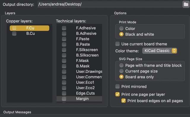
Once the design is done in order to export it I selected the File, export as, SVG I selected only the ‘User.Drawings’ layer for milling and the ‘F.Cu’ layer for the cutting.
Making sure to design a good PCB
Even though this was my first time designing a PCB, I quickly learned some essential design rules the hard way. Here are a few key guidelines to follow before milling and cutting the board:
- Clearance: Pay close attention to the distance between tracks to ensure there is enough room for soldering.
- Width: Ensure there is enough space for the current to flow effectively.
- Footprints: Select the correct footprints for your components, making sure to distinguish between surface-mount and through-hole components.
- Power and Ground: Keep your power and ground tracks separate to avoid short circuits.
- Design: If you're using components like a Xiao RP2040 that need direct connection to a computer, ensure there are no obstructions. This applies to all components; make sure there's enough space for connections and easier soldering.
- Components: Consider how components interact. For example, if you're using a button, ensure you include a resistor in your design.
Selecting the track´s width
Selecting the appropriate track width for a PCB design is crucial for ensuring reliable electrical performance and manufacturability. Here are the key criteria to consider when determining the track width:
- Ampacity: The track width must be sufficient to carry the intended current without overheating. Thicker tracks are needed for higher currents.
- Standards and Calculations: Use IPC-2221 standards or online trace width calculators to determine the appropriate width based on current and acceptable temperature rise.
- Voltage Drop: Wider tracks help reduce voltage drop across the PCB, which is crucial for low-voltage designs.
- Insulation and Clearance: High voltage requires wider tracks to ensure adequate clearance and avoid arcing or breakdown.
- Minimum Track Width: The manufacturing capabilities of your PCB fabricator will dictate the minimum track width and spacing.
- Low current signals (up to 0.5A): 0.1524 mm - 0.254 mm
- Moderate current (0.5A to 1.5A):0.254 mm - 0.508 mm
- High current (above 1.5A): +0.508 mm
Here are some general widths that can be used:
Getting ready the document for milling
In order to cut first the document has to be in the right format so that the machine can read it. For that, I used Mod Project Org where I changed some parameters such as it has been done on week 4.
| Step | Photo | Description |
|---|---|---|
| 1. | Open Mods Project Org | |
| 2. | 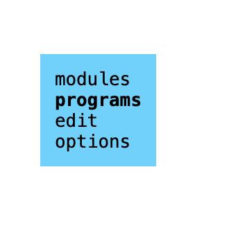 |
Choose “Programs” |
| 3. |  |
Click on “Open program” |
| 4. | 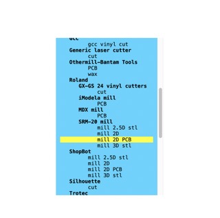 |
Then you have to select the milling machine you are going to use, in my case I selected the Roland/ SRM 20 mill/ Mill 2d PCB |
| 5. | 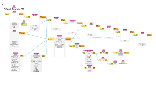 |
It may look like a lot but a handy tip is to start from the left and then go all the way to the right |
| 6. | 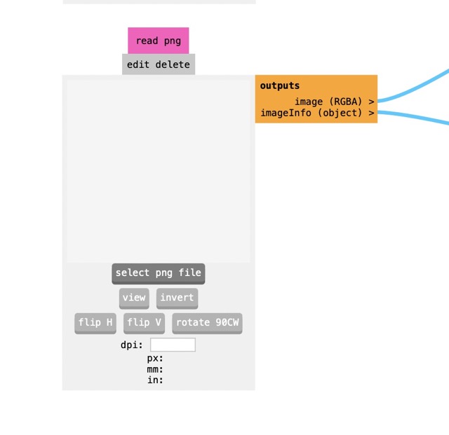 |
In the “Read png pink label” import your png file by clicking “Select png file” |
| 7. | |
After this in the “Convert SG image” option DON’T FORGET TO CLICK “ INVERT”. This is really important since it will invert the colors on the png so that the machine can read the file. If you skip this step the cut will not fit the original size of the file (Trust me I made this mistake) |
| 8. | 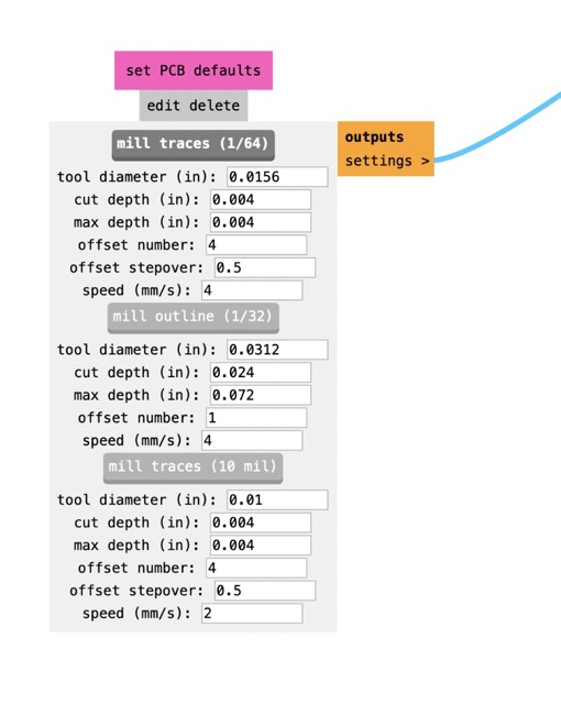 |
Then in the “ Set PCB defaults” pink label click “Mill traces 1/64” so that the png is read as individual vectors to follow throughout the milling process. For the cutting file I selected the "Mill outline 1/32". |
| 9. |  |
In the “Mill raster” feature I chose a “2 offset number” and finally clicked “calculate” |
| 10. | 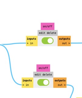 |
Don’t forget to click “on” in the “on/ off” option |
| 11. | Once you finished adjusting the settings return to the “Mill raster” section in step 9 and click “Calculate” so that it automatically saves your file |
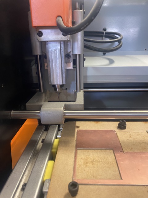
How to use the cutting machine
I used the MONOFAB SRM-20 Milling machine
- Connect the machine to your computer
- Lock your PCB into the machine using the 4 screws and the correct Allen key
- Close the machine’s door
- Turn on the milling machine
- Open the software
- Adjust the X, Y origin by clicking the arrows on the program (Use the cursor step “Continue” for a faster movement)
- Once the end mill is really close to the PCB you can place a Post-it note between it and the PCB, once you can't move the Post-it note, it means the end mill is in the correct Z position
- On the gray part of the window click the “X/Y” button as well as the “Z” one to tell the machine the position in which the end mill currently is, is going to be the new X,Y and Z origin. So that when it starts milling it’ll start on those coordinates.
- Take out the piece of paper and close the machine
- Select the file you want the machine to follow by clicking “cut” which will take you to another window where you can select the file you already edited on Mods Project online
- Press “on” in the spindle feature and click “Z” in the “Move to origin” feature to check if the “Z” position is correct. When you see the material starting to wear out then move down the “Z” origin .1 mm by clicking “x1 in the cursor step feature” and then set that new position as the Z origin (remember this is possible by clicking the “Z” button in the gray space)
- Finally, click “CUT”
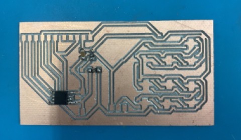
Soldering
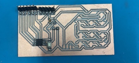
Once the PCB was milled and cut I proceeded to solder all the components. I followed the sketch made in Kicad to know where all the components were supossed to go.
- Attiny 45 Microchip (1)
- 10 k Ohms Resistor (1)
- 2200 Ohms Resistor (1)
- 1 Mf Capacitor (1)
- 1206 Button (1)
- Neopixel Ws 2812 (11)
- Male Pins (14)
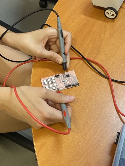

Correct way to measure resistance in a circuit with a multimeter
After attending a class where my teacher explained the basics of PCB design and how to properly use a multimeter, I watched some YouTube tutorials to get the hang of measuring resistance. Here are some steps I found very helpful:
- Ensure the multimeter has its two cables connected (red and black).
- You can either start by measuring resistance from low to high or high to low. I prefer starting from the lower range.
- You should see a 0 or an OL on the multimeter, indicating it's not yet connected to anything.
- Touch the tips of both cables together to make sure the multimeter gets a reading, confirming that it's working.
- Make sure the circuit is not connected to any power source.
- Place the probes on each side of the resistor or the part of the circuit you want to measure.
- If you increase the range on the multimeter, it becomes less detailed, so I recommend starting with a lower range.
- If you don't get a reading, try different ranges until you find one that gives you a result.
Result
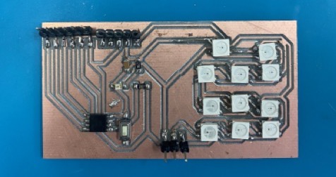
Unfortunately, I solder a neopixel the wrong way and when I tried to desolder it I tore the copper sheet. Because of the deadline I tried to programm it using a cable to close the circuit but I plann to correct that after the assigment is due.
Programming with Arduino
1
Code
For my first code and to learn the basics on how to program neopixels I used an Arduino 1 Board and connected it to the PCB with the Attiny 45. For this I used 3 cables and connected them to voltage, ground and a data pin in both the Arduino board and the PCB.
- I opened Arduino IDE
- Created a new sketch
- Watched a youtube tutorial to learn how to create different loops with neopixels. Youtube Video
- Then I recreated the video's code with the parameters needed for my specific project.
Reflecting on the Assignmen
I enjoyed learning about PCB design, although I must admit it was quite challenging as a complete beginner. Reflecting on this assignment, I realize there is plenty of room for improvement, especially in understanding what each component does. I hope that for my final project’s PCB, I have a better grasp of electrical components and the software. However, once I completed this assignment, I overcame my fear of making mistakes. It gave me the opportunity to delve deeper into electronics design, which I hope to continue.