PCB!
Electronics Production
I’ve never done electronic production before so hearing about PCB was totally new to me. In this week’s assignment I'll take you through the journey that I went through to understand what a PCB is, how to mill it, cut it and solder it. We began with a class focused on the milling machine and the PCB board creation process. During the session, we explored the different types of PCB boards and the materials used to make them. Additionally, we covered critical aspects such as minimum clearance and trace width tolerance. For more detailed information, you can refer to our group assignment page.
What's a PCB anyway?
A PCB, or Printed Circuit Board, is essentially the foundation of most electronic devices, providing a platform for connecting electronic components in a structured and efficient way. In the case of a PCB, the copper traces act as pathways that allow electrical signals to travel between various components, like resistors, which are soldered into the PCB.
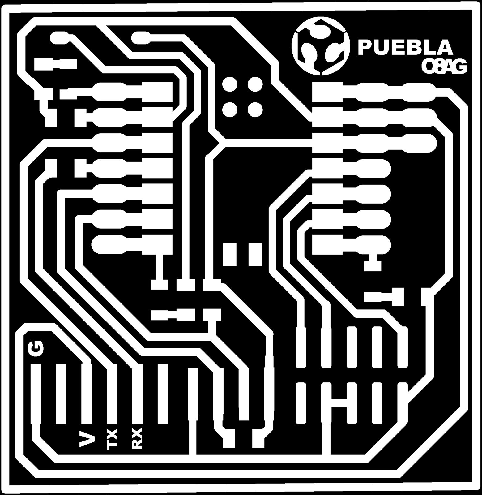
Preparing the document to later mill the PCB
First you need to adjust the document you want to mill into the PCB, for this I used Mods Project Org I’ll take you step by step so that you fully understand how to do it.
| Step | Photo | Description |
|---|---|---|
| 1. | Open Mods Project Org | |
| 2. | Choose “Programs” | |
| 3. |  |
Click on “Open program” |
| 4. | 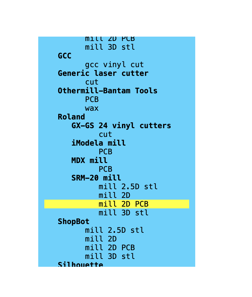 |
Then you have to select the milling machine you are going to use, in my case I selected the Roland/ SRM 20 mill/ Mill 2d PCB |
| 5. | |
It may look like a lot but a handy tip is to start from the left and then go all the way to the right |
| 6. | 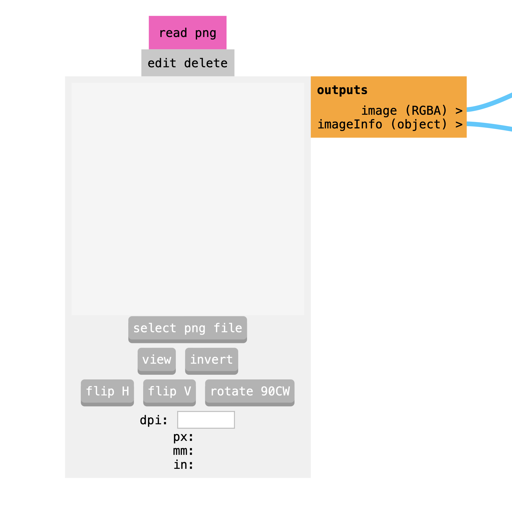 |
In the “Read png pink label” import your png file by clicking “Select png file” |
| 7. | |
After this in the “Convert SG image” option DON’T FORGET TO CLICK “ INVERT”. This is really important since it will invert the colors on the png so that the machine can read the file. If you skip this step the cut will not fit the original size of the file (Trust me I made this mistake) |
| 8. | 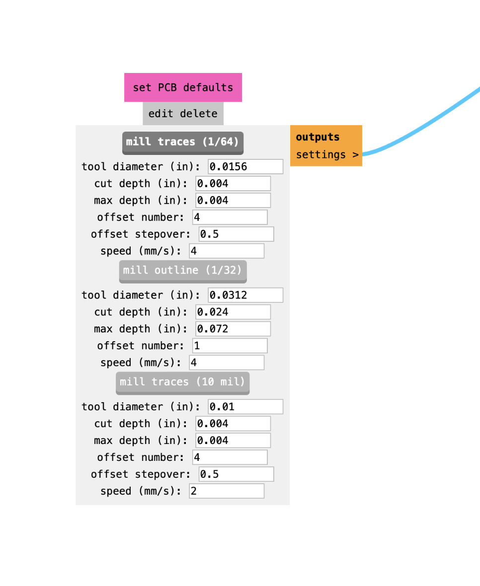 |
Then in the “ Set PCB defaults” pink label click “Mill traces” so that the png is read as individual vectors to follow throughout the milling process |
| 9. | 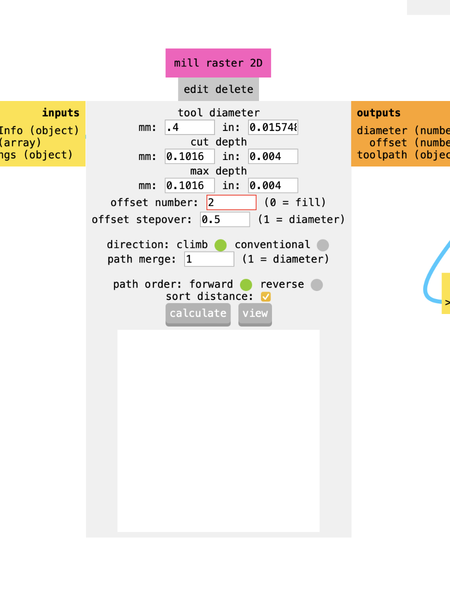 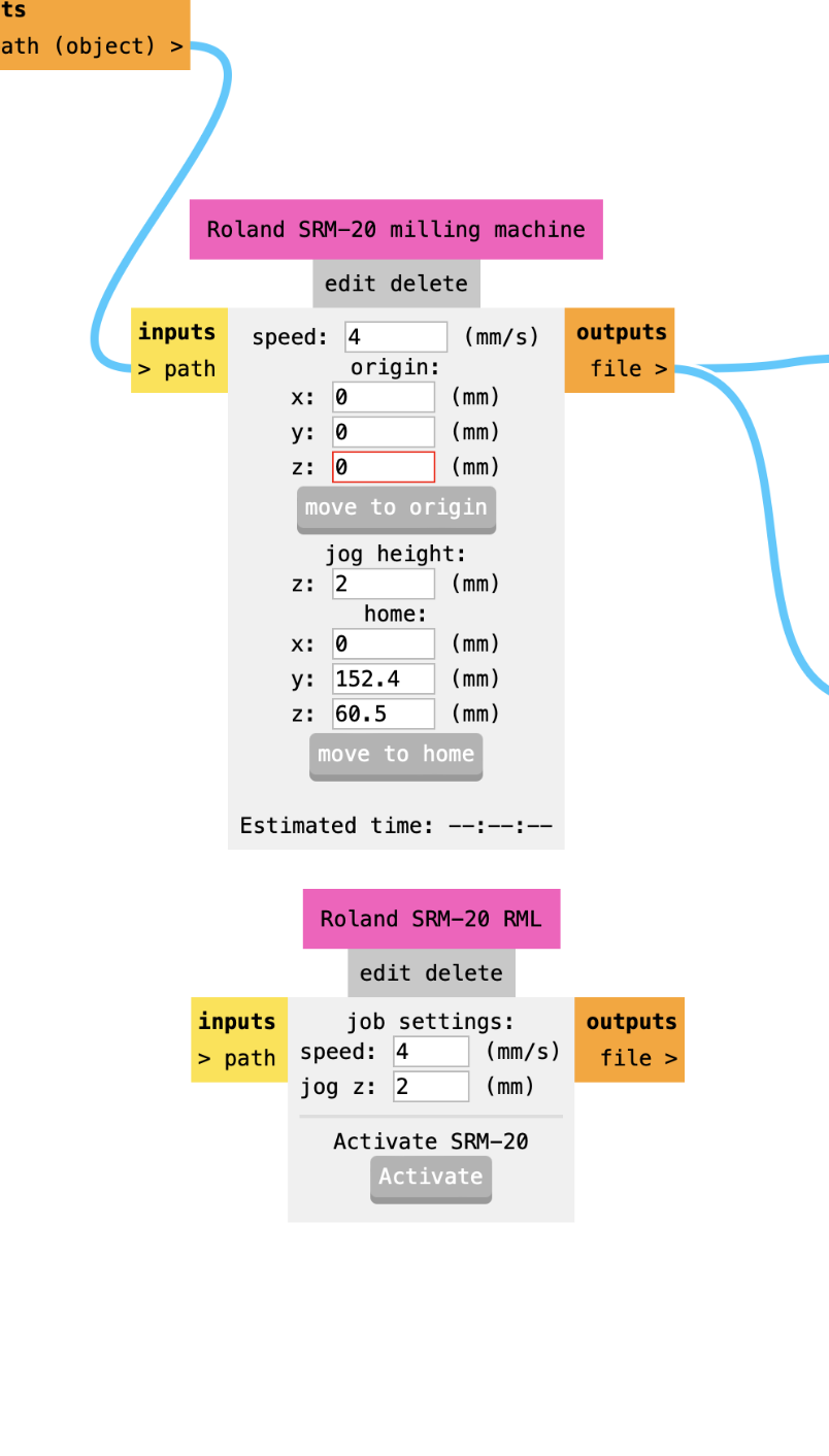 |
In the “Mill raster” feature I chose a “2 offset number” and finally clicked “calculate” |
| 10. | 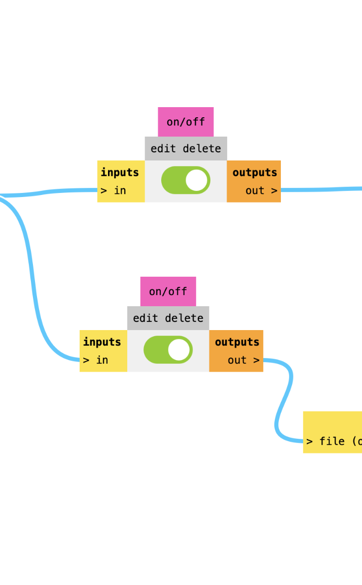 |
Don’t forget to click “on” in the “on/ off” option |
| 11. | Once you finished adjusting the settings return to the “Mill raster” section in step 9 and click “Calculate” so that it automatically saves your file |
Now your file is ready to be used. Don’t forget to follow these steps for both your files, the milling file and the cutting file.
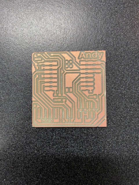
Personalizing your PCB
I used a template provided by my teachers so I wanted to make it my own, in order to do this I used Inkscape. I’ll explain how to edit an existing milling png file.
- First of all, download Inkscape (Fortunately, it is available for iOS)
- Drag and drop the png
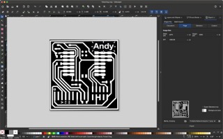
- With the tool bar on the left I simply created a black rectangle to cover the previous design and added my name with the “text” feature
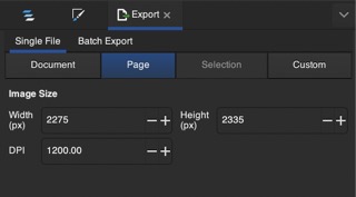
- Click “Export” and change the image size that you need for the PCB in my case I selected a DPI of 1200
- Finally, change the canvas size to the measurements of your PCB and save the png image to later import it into Module Org

What on Earth is DPI?
Before you export the file from Inkscape you need to make sure to export it in the correct DPI because if you don’t the scale of the image will not match the scale of the machine’s file. But to do this we have to understand what DPI is. DPI stands for "Dots Per Inch," and it's a way to measure the resolution of both printed and digital images, but it's more used with printing. Think of DPI as the density of dots in an inch of a printed image. The higher the DPI, the more dots fit into an inch, making a higher resolution image. Now, it's essential to understand that DPI is different from pixels. Pixels are dots that make up a digital image. You can have an image with a set number of pixels, like 8 pixels, and changing its DPI won't change the number of pixels in that image. Pixels represent the image's content, while DPI relates to how densely these pixels are printed.
Why DPI matters?
magine you have an image that's 5 pixels by 5 pixels. No matter what DPI setting you choose, the image will still have 25 pixels in total. But the DPI setting determines how large or small those pixels appear when printed (it determines the total size of the image). For example, if you print this image with a machine set to 5000 DPI, it means the machine is capable of printing 5000 dots in every inch of the paper, but your image still has just 5 pixels. For example: If you tell the printing machine you want a 5 **pixel** image but don't specify the DPI, the machine doesn't have a clear instruction on how big each pixel should be. However, if you set the machine to print at 1000 DPI, you're telling it to fit 1000 dots into every inch, making the physical size of each pixel clear. That means that you’ll get a 5 inch image with 1000 DPI.
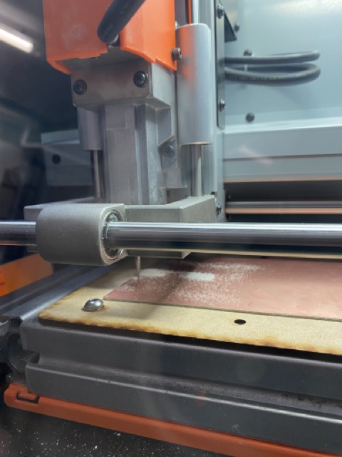
Milling the PCB
I learned how to use a MONOFAB SRM-20 Milling machine. It basically works as a CNC router but smaller. First thing you need to do is download the software to control the machine. Since it is not available for Mac I had to borrow someone else´s computer to do it. Let’s get going!
- Download the V panel for SRM 20
- Download the driver for the Windows software update you have
- Connect the machine to your computer
- Lock your PCB into the machine using the 4 screws and the correct Allen key
- Close the machine’s door
- Turn on the milling machine
- Open the software
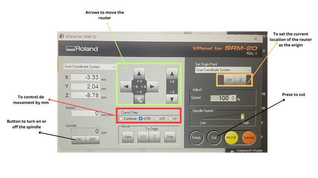
- Adjust the X, Y origin by clicking the arrows on the program (Use the cursor step “Continue” for a faster movement)
- Once the end mill is really close to the PCB you can place a Post-it note between it and the PCB, once you can't move the Post-it note, it means the end mill is in the correct Z position
- On the gray part of the window click the “X/Y” button as well as the “Z” one to tell the machine the position in which the end mill currently is, is going to be the new X,Y and Z origin. So that when it starts milling it’ll start on those coordinates.
- Take out the piece of paper and close the machine
- Select the file you want the machine to follow by clicking “cut” which will take you to another window where you can select the file you already edited on Mods Project online
- Press “on” in the spindle feature and click “Z” in the “Move to origin” feature to check if the “Z” position is correct. When you see the material starting to wear out then move down the “Z” origin .1 mm by clicking “x1 in the cursor step feature” and then set that new position as the Z origin (remember this is possible by clicking the “Z” button in the gray space)
- Finally, click “CUT”
How to cut the PCB once it is already Milled
To cut the PCB repeat the steps stated before but choosing the cutting file instead of the milling one. REMEMBER you need to change the milling end to a cutting one!
If you get it right on the first try you miss the opportunity to fully learn!
1
First Try
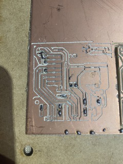
On my first try I followed all the steps previously listed, nevertheless the resulting paths on the PCB were very narrow. This was caused because of the “Z origin” which was way deeper than it should’ve (should have been).
2
Second Try
Since I had to do it all over again, I decided to personalized my PCB (I explained how I did it previously). But when it was the time to mill it I accidentally forgot to invert the cutting image in Mods Org online. So as a result the machine cut inside the shape instead of outside, which caused the PCB to be smaller than it should’ve.
3
Third Try
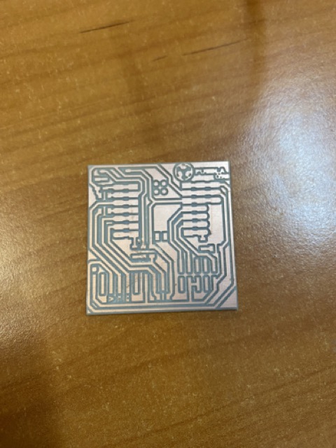
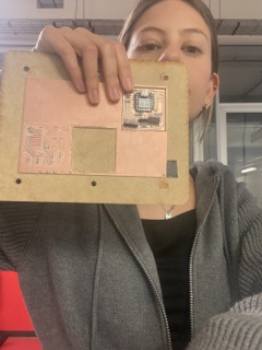
On the third try unfortunately I couldn’t use my personalized PCB since I didn’t have the file and since I don’t own a Windows computer I had to cease the opportunity to use my teacher’s when it was available. On the bright side, this third PCB turned out okay.
4
Fourth Try
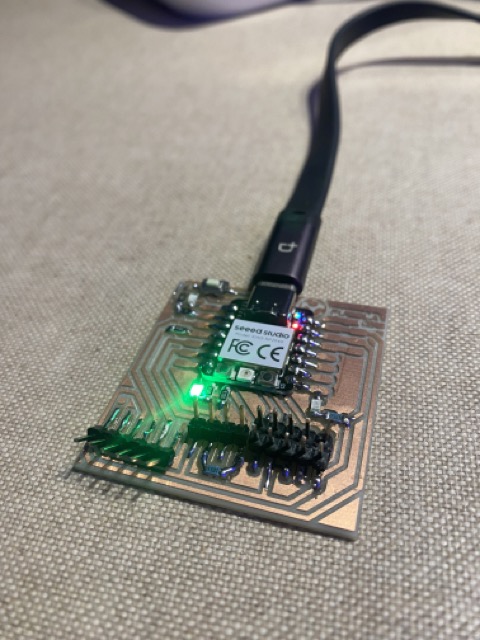
Unfortunately, after doing all the programming 2 of the leds didn’t turn on. It was because of the soldering in the leds circuits it wasn't fully touching like it should.
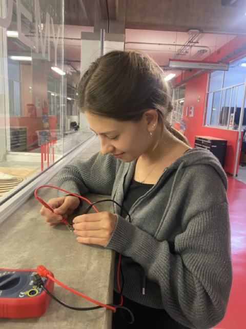
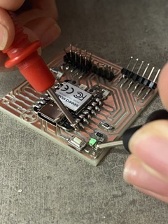
Soldering
It is harder than it looks!
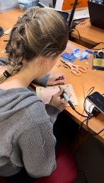
The trick to soldering correctly is to heat the copper clad and then place the solder on top of it. Do not place the soldering iron directly into the solder.
Programming with Arduino
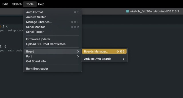
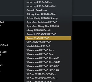
First, I added the Seeed Studio XIAO RP2040 board package to my Arduino IDE by
- Going to ‘Preferences’ and in ‘Aditional boards manager URLs’ pasting this link: https://github.com/earlephilhower/arduino-pico/releases/download/global/package_rp2040_index.json
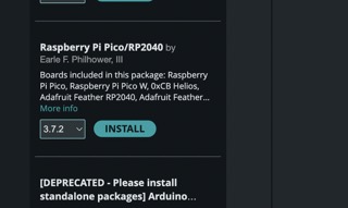
- Then clicking under Tools > Boards > Board Manager and typing ‘RP2040’ and selecting ‘Raspberry Pi Pico/RP2040’ to install it
To program my PCB I did the following things:
- First I downloade Arduino IDE for IOS. Then in the “tools” menu on the menu bar, I selected the option “Board” and the “Board manager”. Finally, I selected “Raspberry Pi Pico/RP2040” and then the “Seed Xiao RP2040”.
- Then, I connected the PCB to my computer and on the “Board menu”, clicked on the “Port” feature and selected the “USB modem”.
- After that, I downloaded the Arduino file that my teachers gave me into the program and proceeded to click the “Upload arrow”.

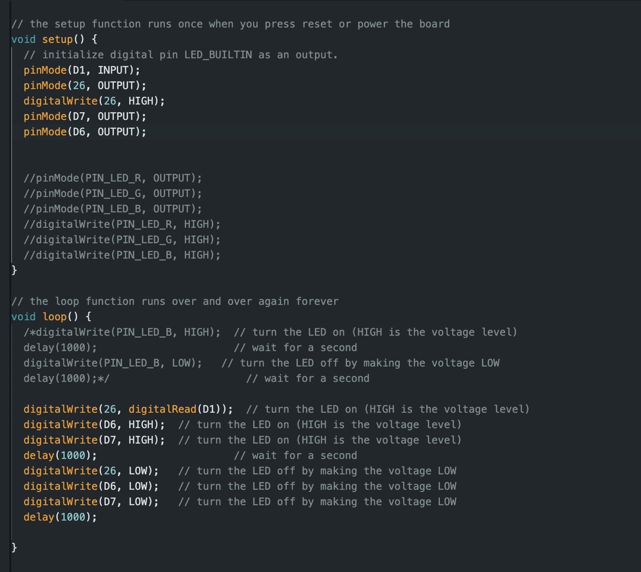
CODE
Results
Tips for getting the PCB to turn out okay
- Make sure your images are inverted
- Use a paper to make sure the “Z origin” is at the correct height and then turn on the spindle and cut slightly into the material to set the “Z” origin .1mm below the surface of the copper clad sheet
- Make sure to change the end mill for cutting
- Don’t forget to save your images with the correct DPI
Process Evidence
WHAT I LEARNED FROM THIS ASSIGMENT
This week was challenging as I had never milled or soldered a PCB before. It took me some time to grasp the logic behind PCB design and its components. The milling process may not seem difficult, but it is quite challenging, especially for beginners. It's crucial to follow the steps I wrote in Mods Org precisely. I found that setting the Z origin correctly is the most difficult part because if it's done incorrectly, the tracks can turn out too slim. Soldering was also new to me, and I initially started off on the wrong foot. I quickly learned that it's not about using as much solder as possible but rather about doing it neatly. I also learned about DPI, and after a lot of explanation, I understood its logic. It's a concept that's really important for PCB design. Despite the difficulties, I enjoyed this assignment and look forward to getting more involved in programming and experimenting with PCBs in the future.