Electronics Design
Objectives for Week 8
- Use an EDA tool to design a development board to interact and communicate with an embedded microcontroller, produce it, and test it
extra credit: try another design workflow, design a case for it and simulate its operation
- Group Assignment: Use the test equipment in your lab to observe the operation of a microcontroller circuit board
Group Assignment
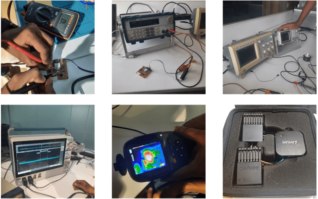
This week's group assingment was to use the test equipments in our lab to observe the operation of a microcontroller circuit board.
For further details, click on the link below.
Group Assignment-Week 8PCB Design
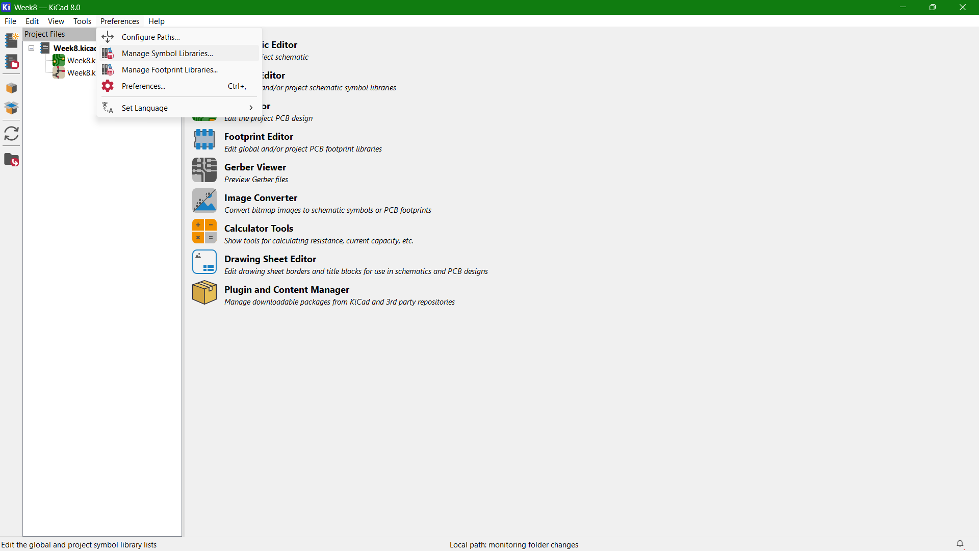
This week started off with a session by our instructor, Saheen. He explained the basics of electronics as well as the basic equipments that will be required during the process and its working. Since, this week is about designing a PCB, I was scared at first as I don't have much experience in it but our instructor walked us through each steps and helped us when we were stuck. For designing the PCB, we were introduced to KiCad.
KiCad
KiCad is an open-source Electronic Design Automation (EDA) software. The software facilitates schematic designing of electronic circuits as well as their conversion to PCB layouts. Click here to download KiCad.
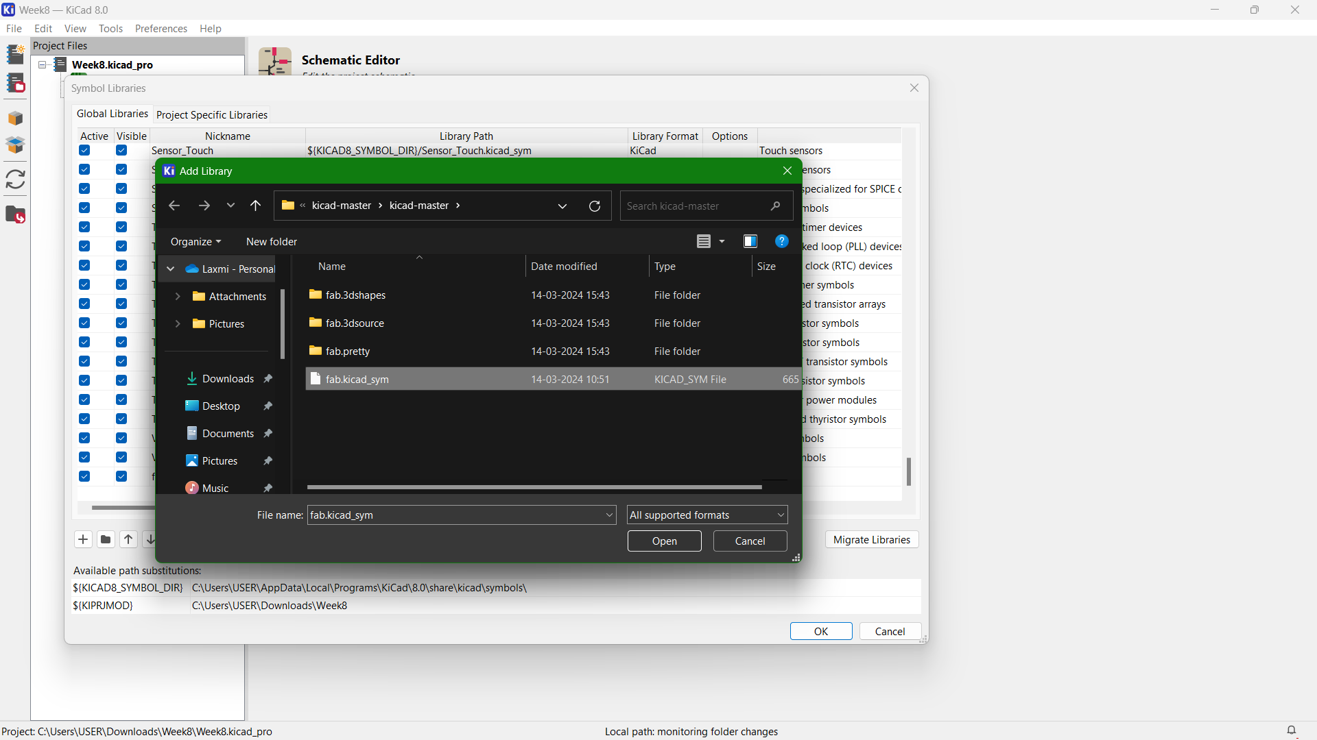
I created a new project "Week8". Fab Academy has its own library of symbols and footprints for KiCad. So, I downloaded the .zip file from the below link.
https://gitlab.fabcloud.org/pub/libraries/electronics/kicadTo insert the symbols file, open KiCad, then follow Preferences > Manage Symbol Libraries > Add file
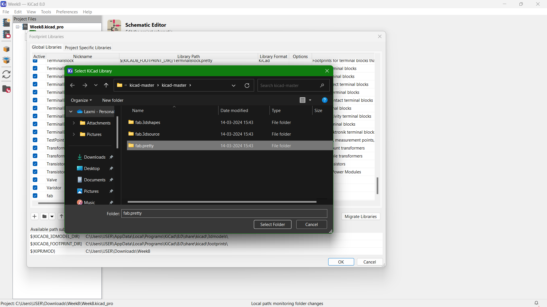
To insert the footprints file, go to Preferences > Manage Footprints Libraries > Add file
To insert the footprints file, go to Preferences > Manage Footprints Libraries > Add file
For this week, I chose SAMD11C microcontroller for my design. SAMD11C is a series of low-power microcontrollers based on ARM Architecture.ARM architecture specifies a set of rules that define how the software and hardware interacts with each other and how hardware works when an instruction is executed.
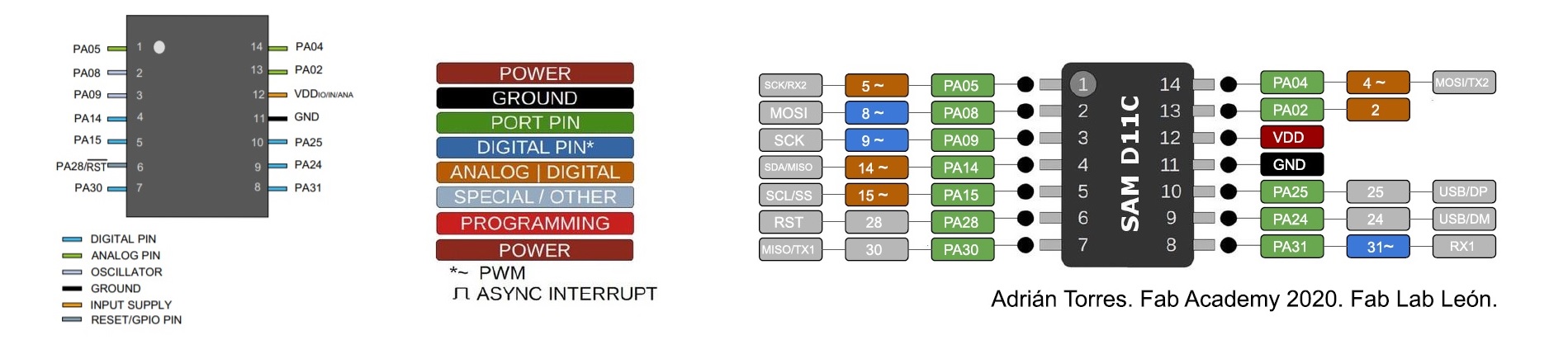
Features of SAMD11C:
- 16KB of flash memory
- Variety of input/output options including GPIO (General Purpose Input Output) pins, I2C, SPI, and USART interfaces for serial communication (for connecting to other devices and sensors)
- 16-bit timers, PWM (Pulse Width Modulation) capability (for controlling motors or LEDs, and real-time counters)
- 4KB data storage
- 10-bit Analog-to-Digital Converter (ADC)
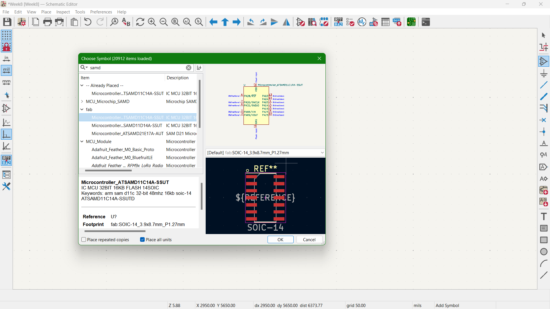
I opened the schematic file and started adding the components required for my design. Press "a" to add the symbols and all the symbols I wanted were there under the "fab" group.
Schematic Diagram
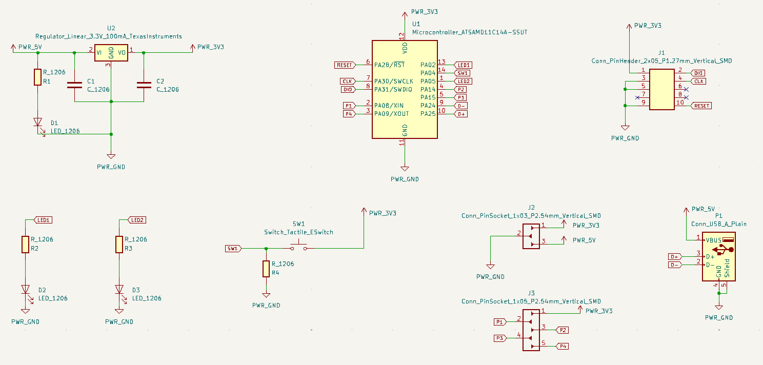
Components
- SAMD11C14A Microcontroller
- Voltage Regulator 3.3V 100mA
- LED 1206 (x3)
- Resistor 1206 (x3)
- Tactile Switch
- Capacitor 1206 (x2)
- Conn Header 10pos Vertical SMD
- Conn PinSocket 5pos Vertical SMD
- Conn PinSocket 3pos Vertical SMD
- USB Type-C Connector
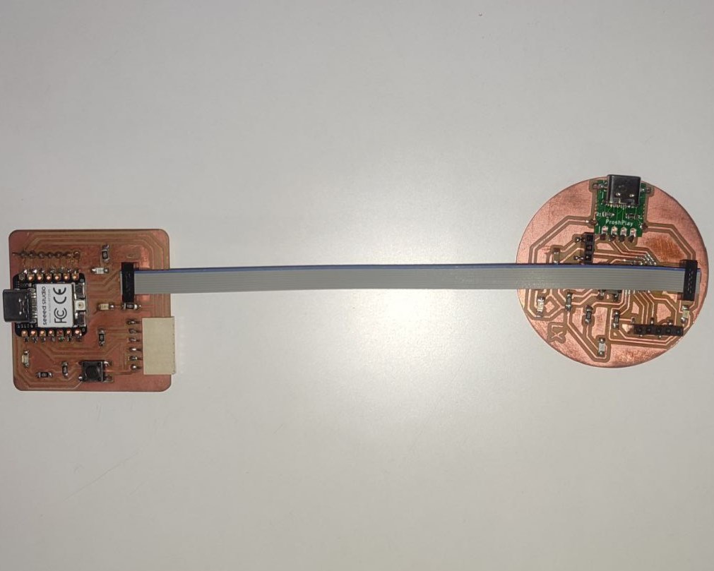
I used the breakout board I have soldered during Week 4 for my work here.
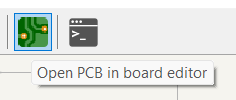
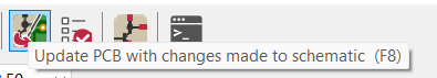
Once the schematic diagram was complete, next step it to design the PCB and add the traces. For that, click on the Open PCB in board editor icon at the top right.
Then a new screen opens up and to update the PCB click on the Update PCB with changes made to schematic icon at the top right. Press "Update PCB".
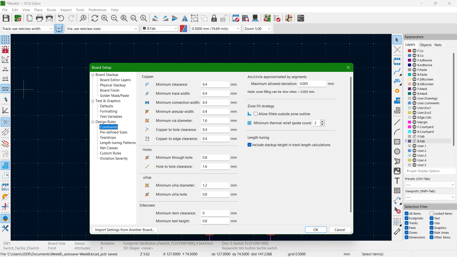
Next step is to define the constraints and parameters for the PCB designing. According to the capability of our milling machine that has been identified during the "Electronics Production" week, the values are as below:
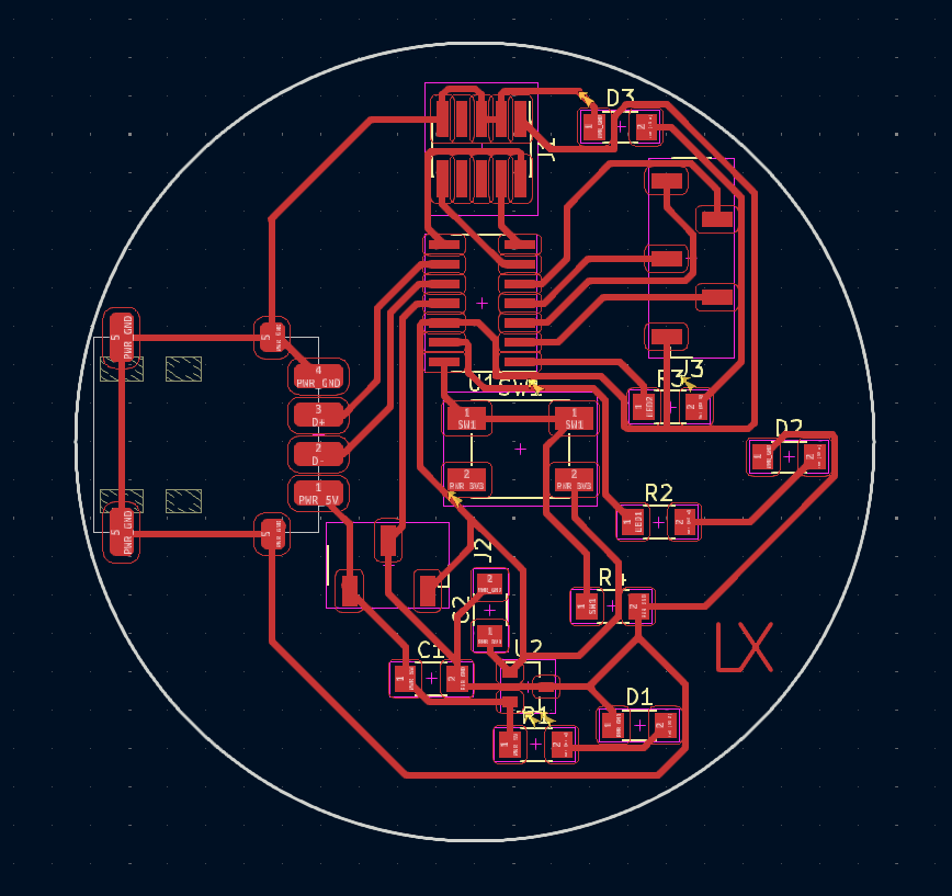
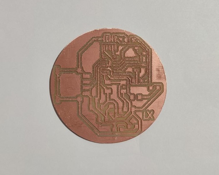
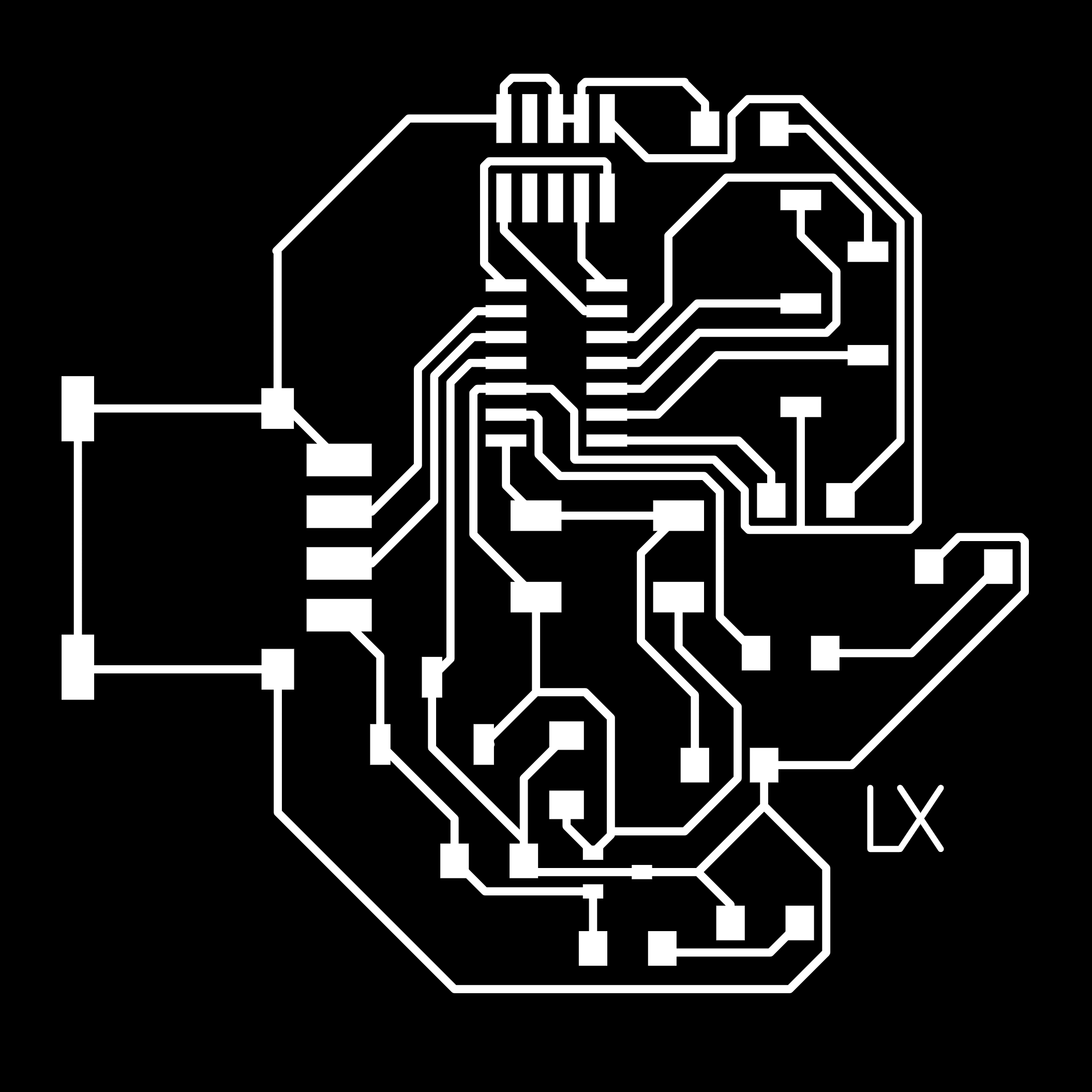
Then I started the long process of drawing the traces for the PCB. It was my first try at this task and it was interesting at first. It seemed just like a maze, where, you have to find a path for each connections without crossing another.
1 hour later.. fixing. 🙂
2 hours later.. still fixing. 😐
3 hours later...... STILL fixing. 🫥
My instructor helped me in between as my mind goes blank after a particular interval of time and I stare at the PCB with despair 🥹. It took me a total of 6 hours to finally get this done and the satisfaction I received has no words. Respect to those who do this on a daily basis!🫡 I enclosed my design with a circle and this is how my PCB design turned out.
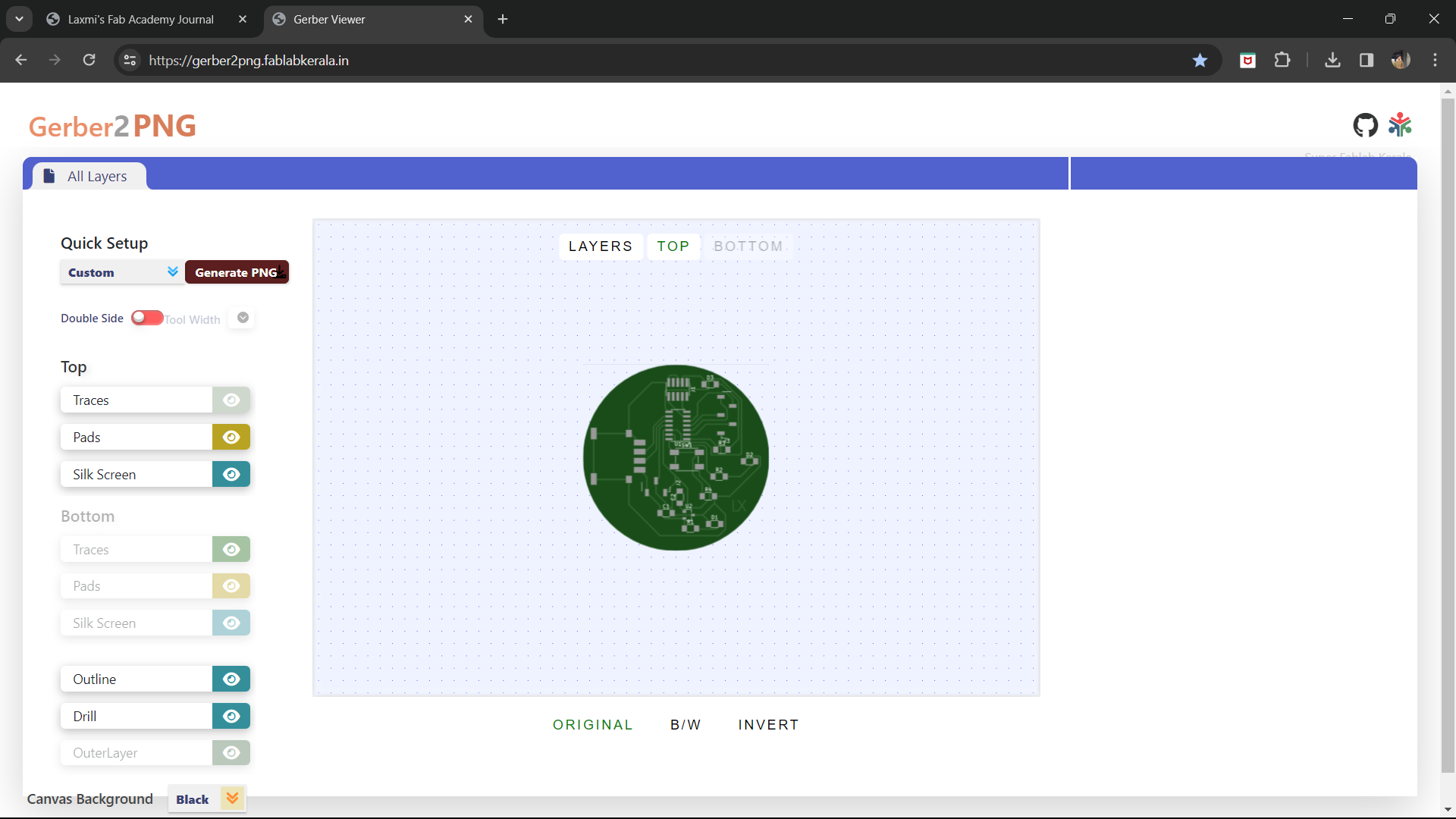
The next step is to mill the PCB. For that we need the file in either .png or .svg file format. But it cannot be done directly from KiCad. So, our fablab, Super FabLab Kochi, has created an online software to convert gerber files to png.
Gerber Viewer converts gerber files into png file format. I first exported the PCB design as gerber. Then imported all the files to gerber view.
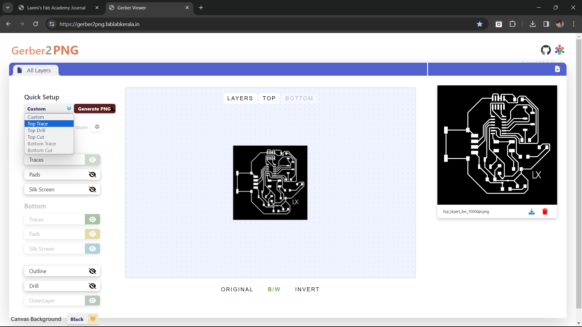
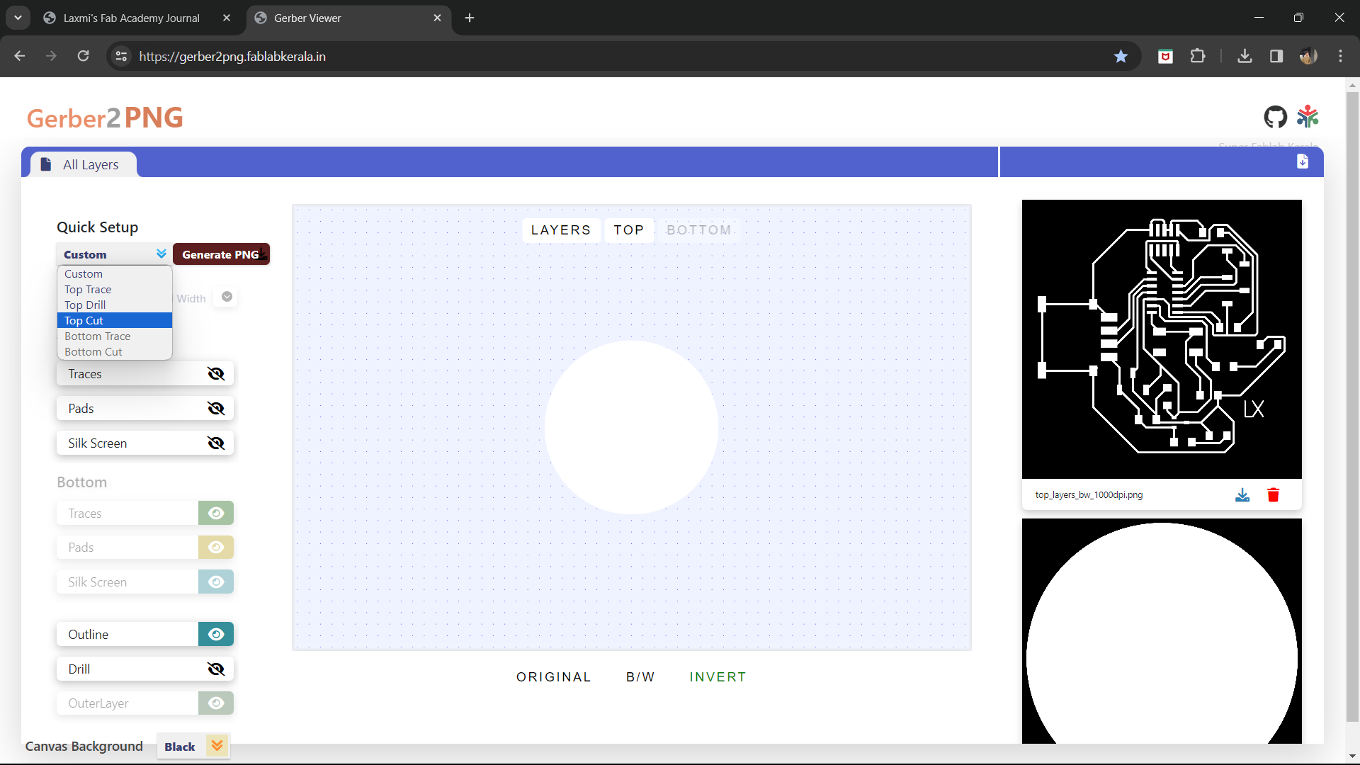
Next, I selected Top Trace from the option and clicked on "Generate PNG". For the edge cut, I selected Top Cut.
PCB Milling
The next step is milling the PCB. I am using Roland Modela MDX20 along with MODs for the purpose. I already have some experience in using both during "Electronics Production" week.
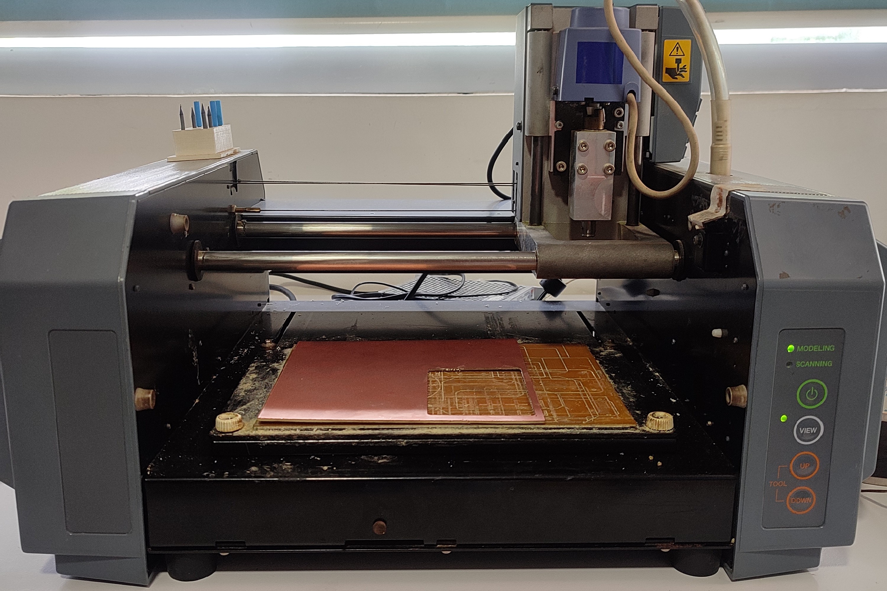
Refer documentation of Week 4 to know about the working processes of Roland Modela MDX20 and MODs.
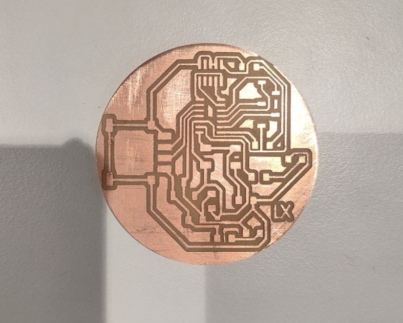
The finish after milling wasn't great. So I sanded down the PCB and here's how it turned out.
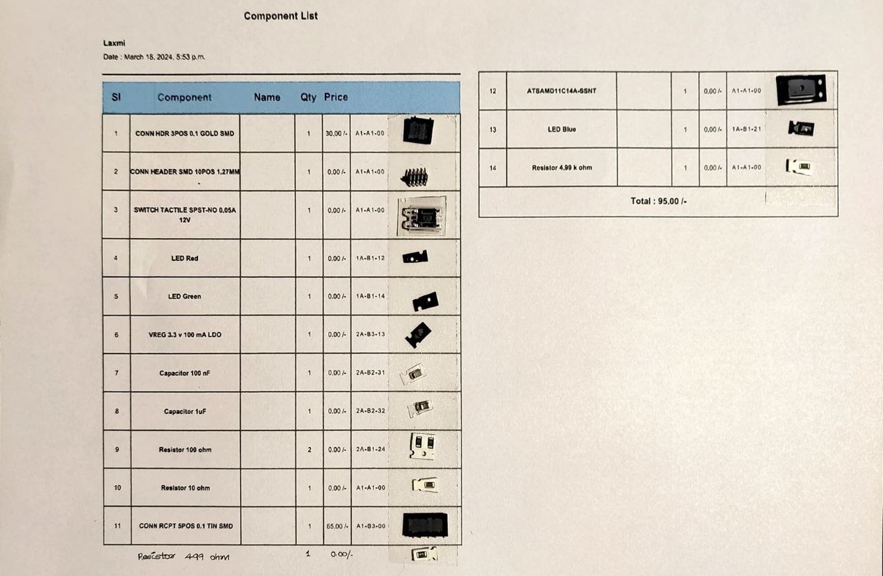
The next step is to request for the required components from Fab Inventory. Before requesting, I first had to calculate the resistor and capacitor values. I used DigiKey for the calculation.
 R1= 499 ohm
 R2= 10 ohm
 R3= 100 ohm
 R4= 4.9k ohm
 C1= 1 µF
 C2= 100 nF
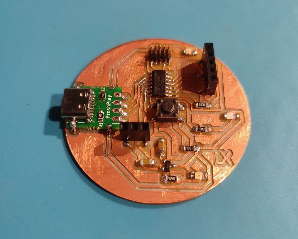
During "Electronics Production" week I was introduced to soldering and it was a great experience and I was looking forward to it this time.
Here's the final outcome:
Programming
To use the PCB, first we have to flash the bootloader. For that we are using the Quentorres board as the programmer. I followed the steps provided in the Quentorres documentation to make the board as programmer. First, I connected the Quentorres board to the new board using a 10 pin connector.
Next I pasted the below link to add the board in Arduino IDE.
https://raw.githubusercontent.com/qbolsee/ArduinoCore-fab-sam/master/json/package_Fab_SAM_index.jsonI installed the below file from the "Board Library".
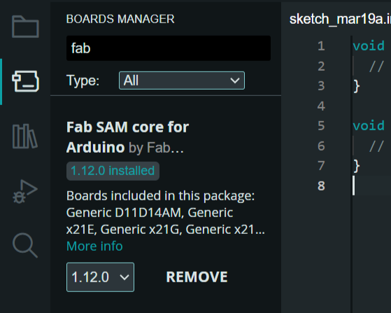
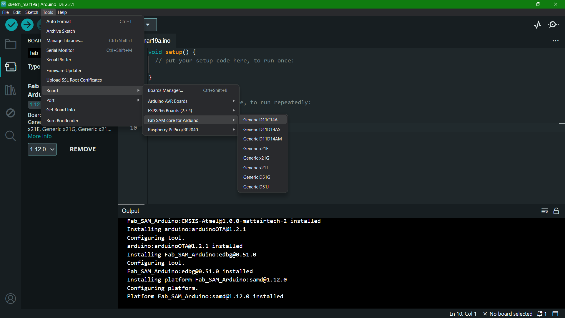
Next I selected the board from Tools > Board > Fab SAM core for Arduino > Generic D11C14A.
The programmer was changed to CMSIS-DAP.
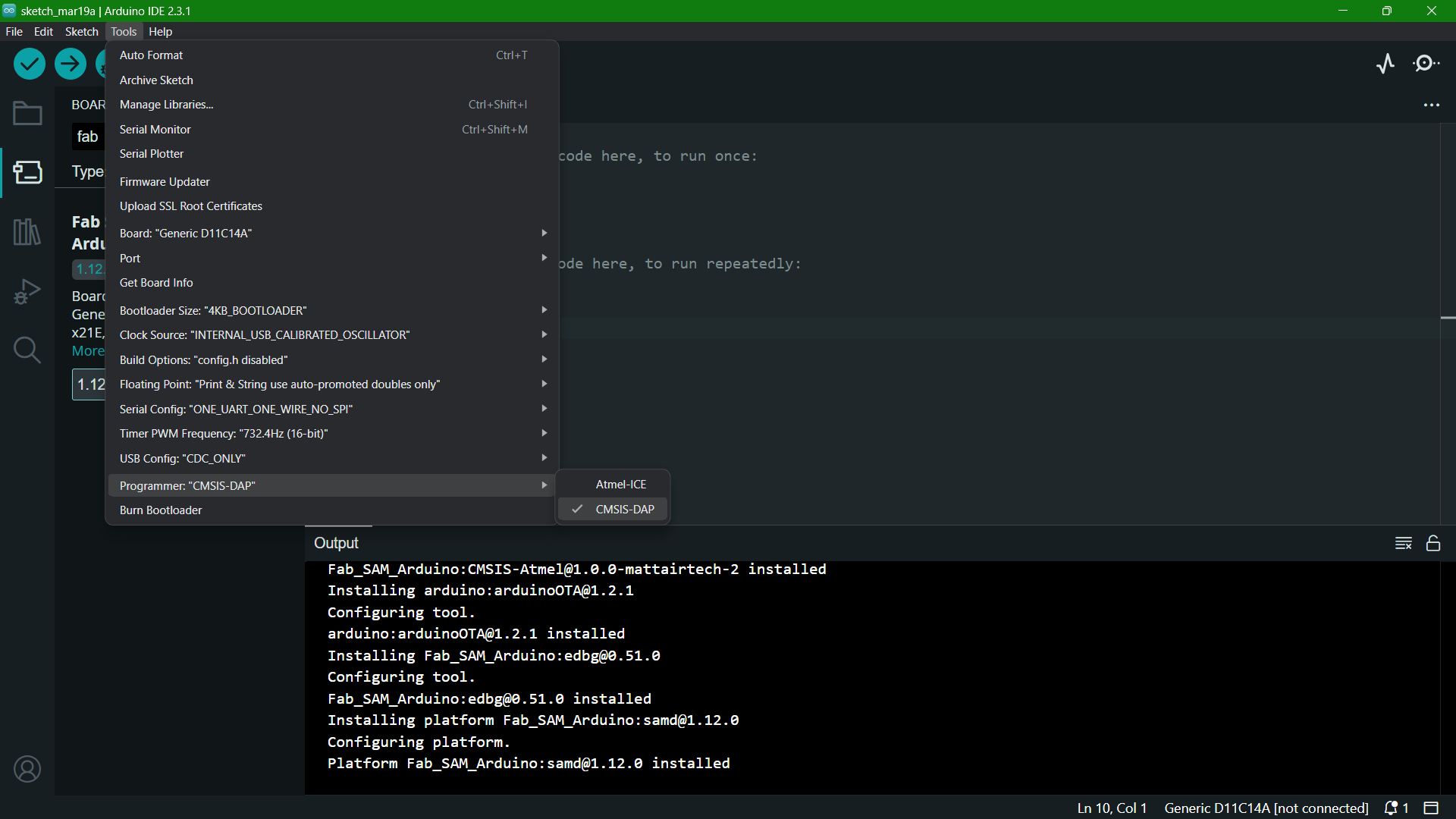
Then I clicked on Burn Bootloader.
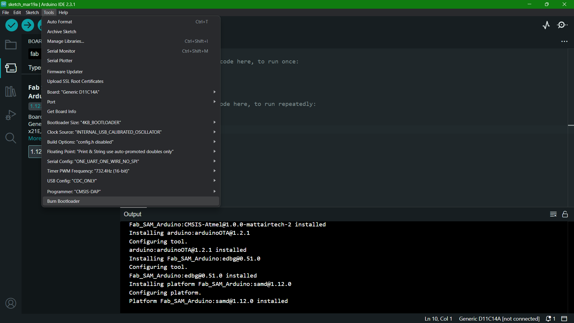
And the bootloader has been burned.
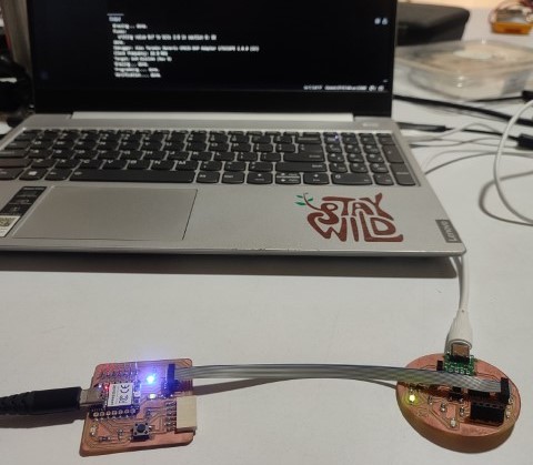
Now the new board is fit to use. I ran a code I had already done during the "Embedded Programming" week, where, the LEDs are lit sequentially on a button press. I just had to change the pin number of the LEDs and the button.
Code to light up 2 LEDs sequentially on button press
    const int buttonPin = 4; // Button pin from SAMD11C14A (refer schematic diagram)
    const int ledPins[] = {2,5}; // LED pins from SAMD11C14A (refer schematic diagram)
    const int numLeds = 2; // Number of LEDs
    int ledIndex = 0; // Current LED index
    bool previousButtonState = HIGH; // Previous button state, assuming pull-up

    void setup() {
      for (int i = 0; i < numLeds; i++)
      {
        pinMode(ledPins[i], OUTPUT); // Initialize LED pins as output
      }
      pinMode(buttonPin, INPUT_PULLUP); // Initialize button pin as input with pull-up resistor
    }

    void loop() {
      bool currentButtonState = digitalRead(buttonPin);
      if (currentButtonState == LOW && previousButtonState == HIGH) {
        // Button was pressed
        blinkLedsRecursively(0); // Start blinking sequence
      }
      previousButtonState = currentButtonState; // Update the previous button state
    }

    void blinkLedsRecursively(int index) //recursive function
    {
      if (index >= numLeds) return; // Base case: stop if past the last LED

      digitalWrite(ledPins[index], HIGH); // Turn on current LED
      delay(500); // Wait for half a second
      digitalWrite(ledPins[index], LOW); // Turn off current LED

      blinkLedsRecursively(index + 1); // Recursively call for the next LED
    }
Download Files
  • PCB Design Files (zip)
  • PCB Trace (png)
  • PCB Cut (png)