Electronics Production
Objectives for Week 4
- Make and test a microcontroller developement board
- Group Assignment: Characterize the design rules for your in-house PCB production process send a PCB out to a board house
Group Assignment
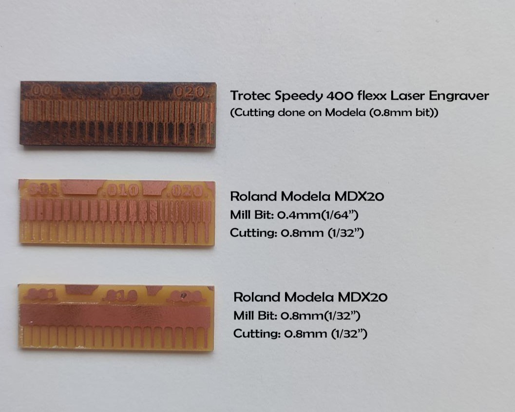
The group assignment for this week was to characterize the design rules for the in-house PCB production process. We attempted to mill the traces in PCB using both Roland Modela MDX20 and Trotec Speedy 400 flexx Fibre Laser Engraver. Here's the result:
For more detailed explanation, click on the link below.
Group Assignment-Week 4Printed Circuit Board (PCB)
A printed circuit board (PCB) is a flat, rigid board made of non-conductive material, usually fiberglass, with thin layers of copper foil laminated onto one or both sides. The copper foil is etched to create a network of electrical pathways, or traces, that interconnect electronic components mounted on the board. The components are soldered to the traces, creating a complete electronic circuit. PCBs are used in virtually all electronic devices, from simple toys to complex computers.
For the in-house production of PCB, we used FR-1 material, which is a combination of paper laminates covered by thin copper layer. It is less harmful than using a fibre glass (FR-4), since, for FR-4, the etching process involves using strong chemicals that can be harmful if not handled properly. Proper ventilation, personal protective equipment (PPE), and safe disposal of spent etchant are crucial.
PCB Design
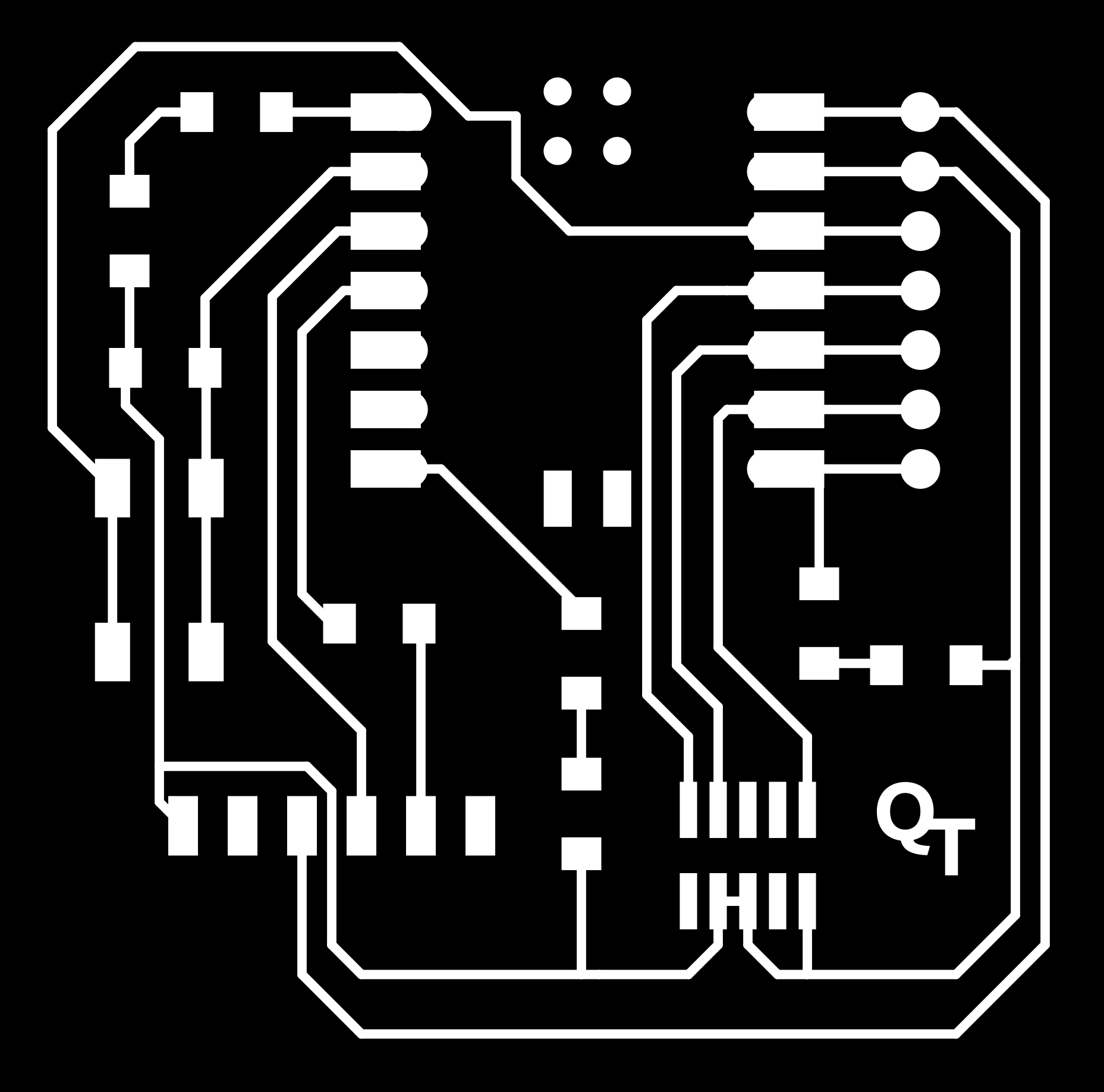
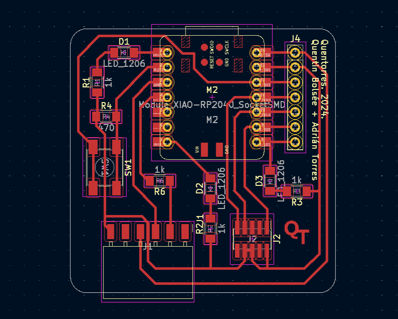
This week's assignment involved making a microcontroller development board. The first step was to design and mill the PCB. I downloaded the PCB design of the Quentorres (version 1) provided on Fabcloud. The files provided included the traces, interior, and the portions to be drilled.
Quentorres board was created by Quentin Bolsée and redesigned by Adrián Torres in 2024 during Instructors Bootcamp in León. This versatile board is designed to program new AVR (Automatic Voltage Regulators) Series 1 and 2, as well as ARM (Advanced RISC Machines) microcontrollers. It includes a button and LEDs for basic input and output functionality, and features breakout pins for connecting additional external elements.
I wanted to customize the board. So, I used Gimp to make my changes. I imported the file into Gimp.
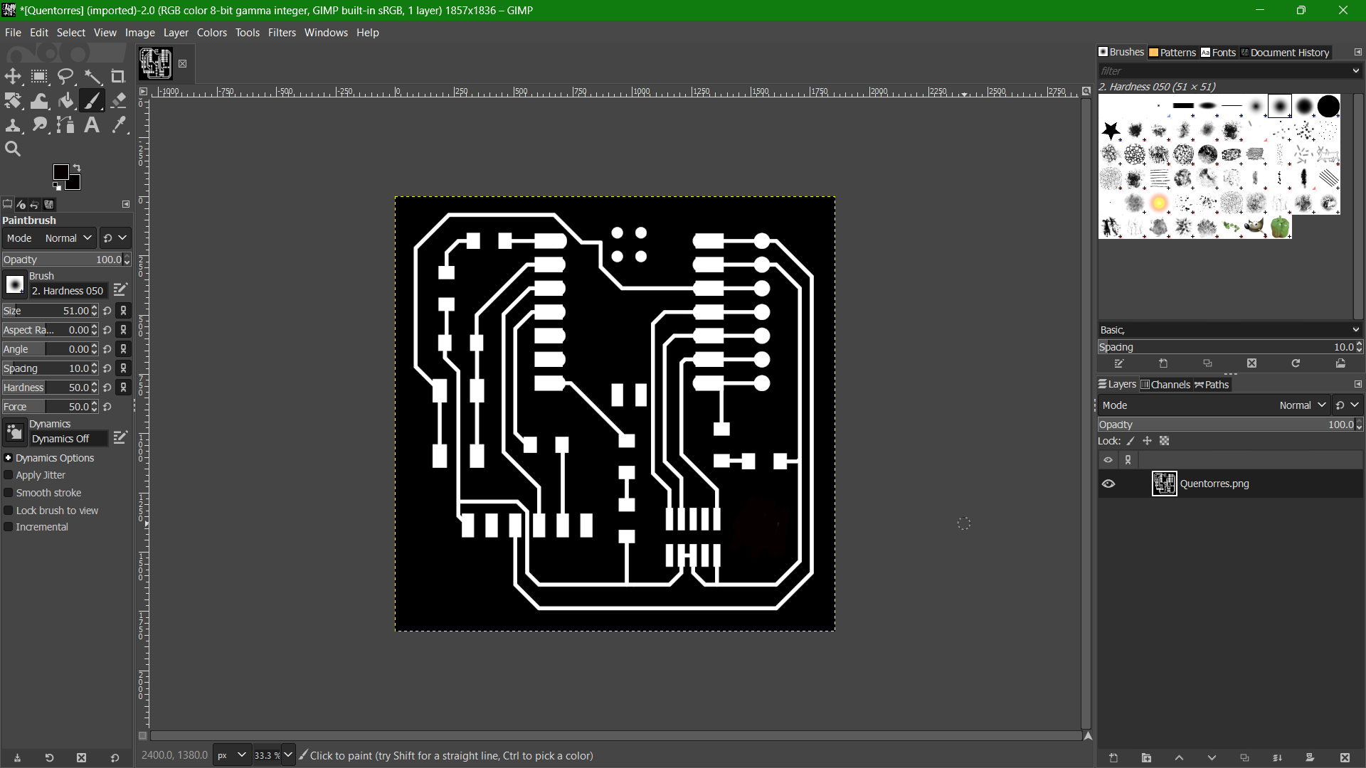
I then used the brush tool to remove the Quentorres signature. After that, I added mine.
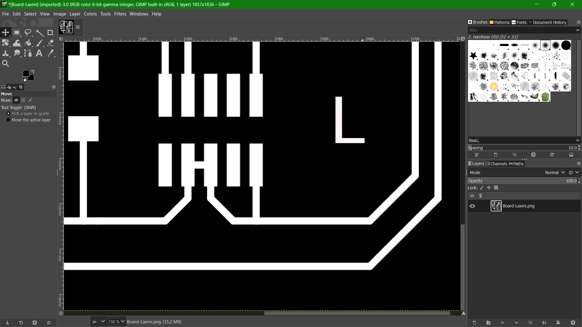
Once I was satisfied with the result, I exported the image as .png file.
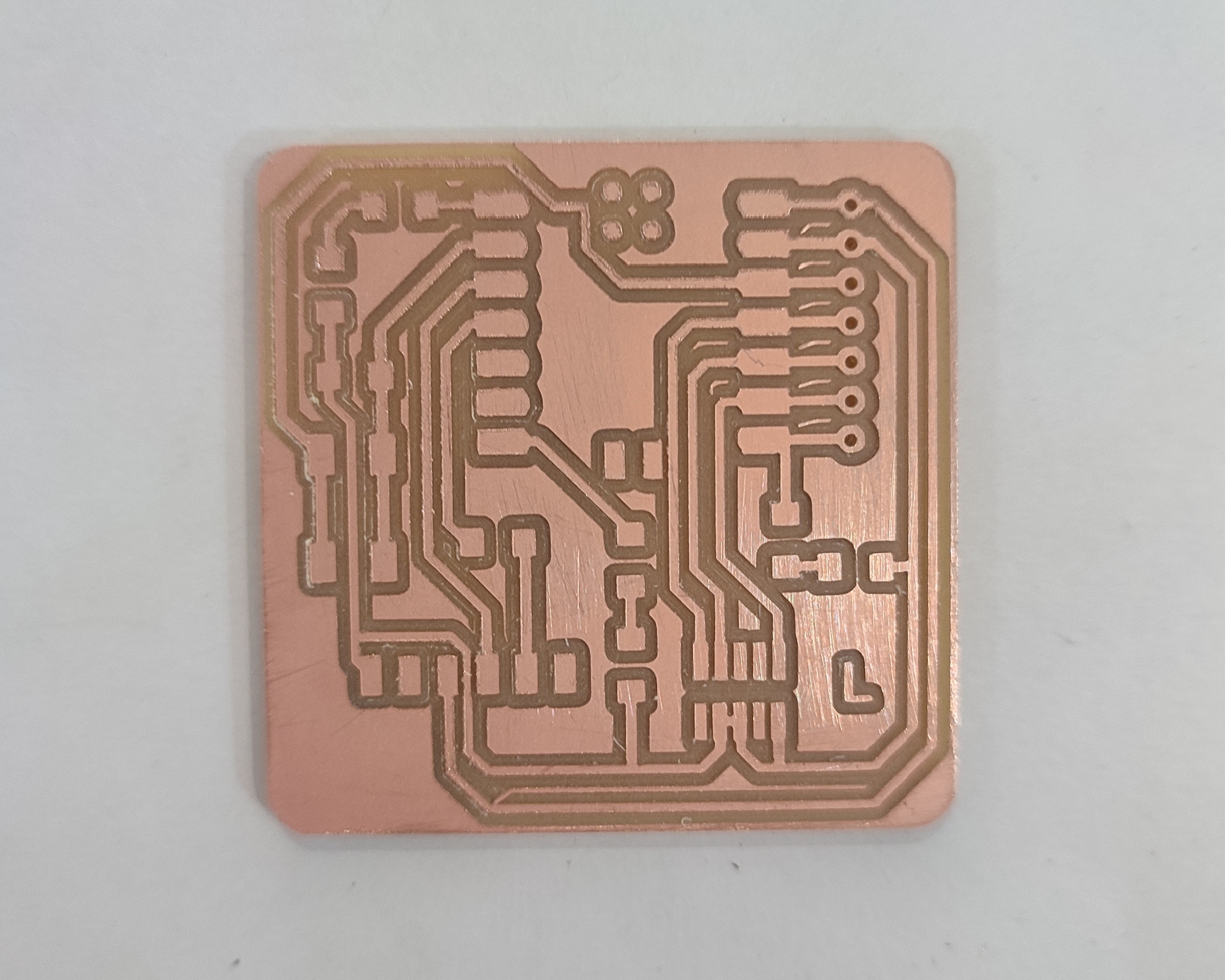
PCB Milling
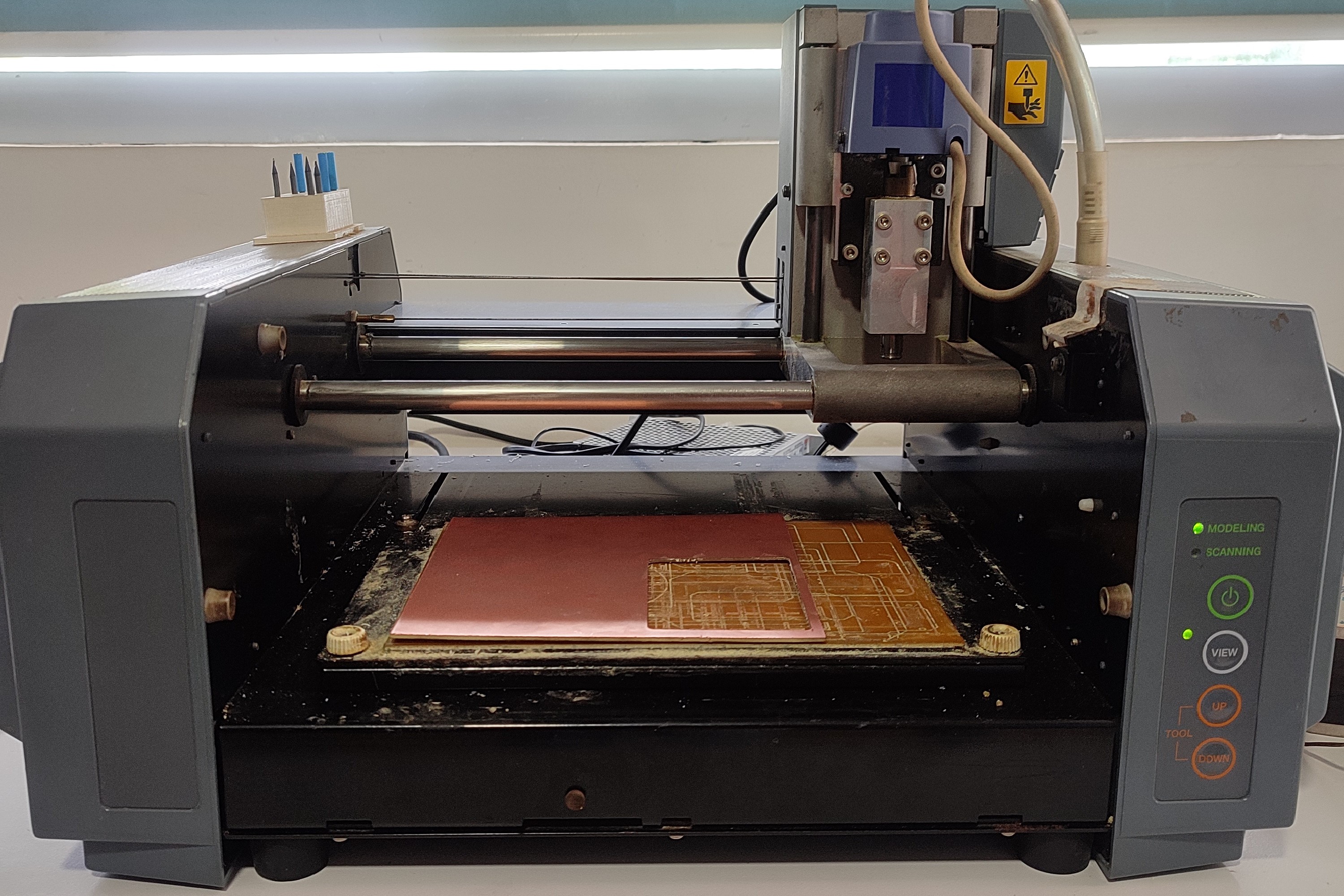
The next process is to mill the traces on the PCB board. We have Roland Modela MDX20 in our Fablab. The MDX-20 can mill away unwanted copper from a pre-laminated copper-clad fiberglass board, creating the desired circuit traces.
We use MODs to control the machine. I already have some experience in using MODs during the third week for vinyl cutting. I imported my trace file to MODs.
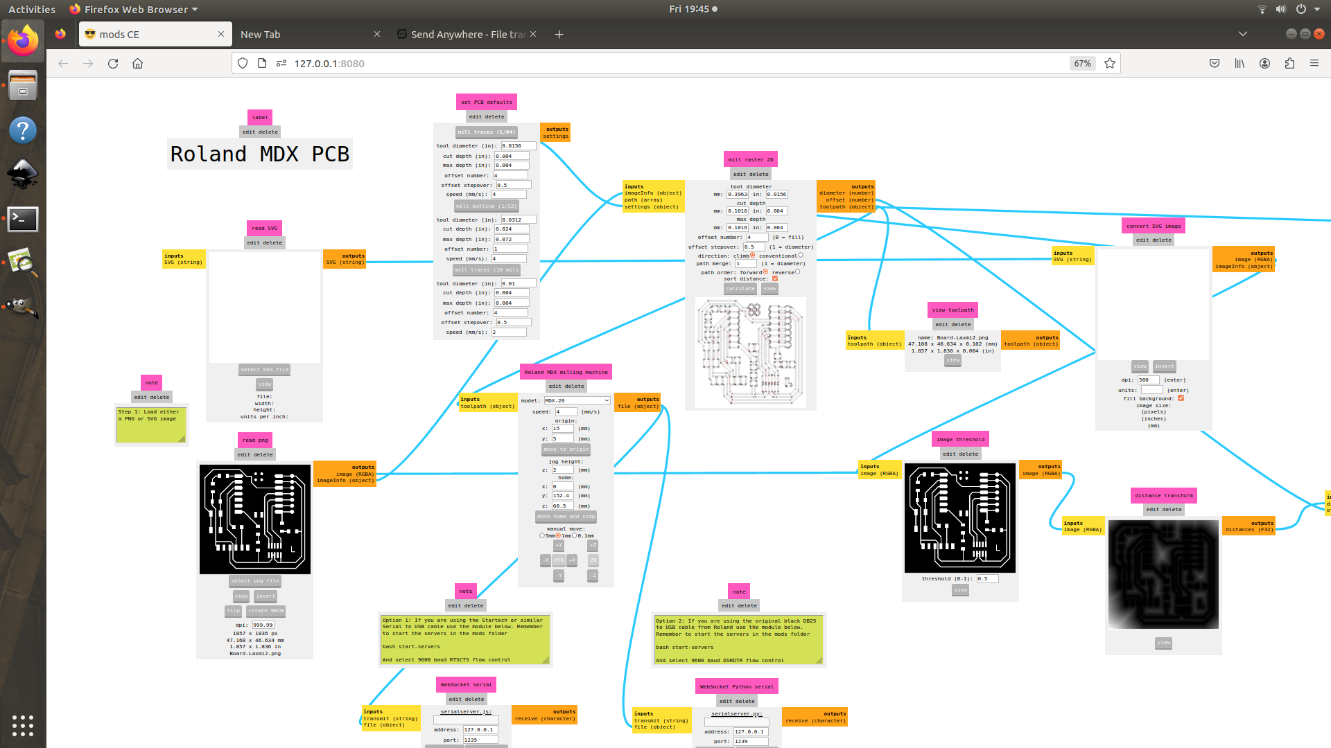
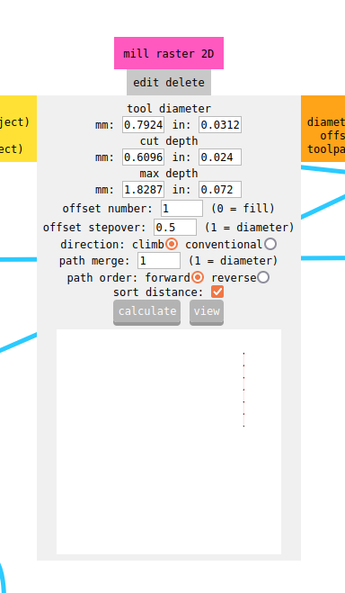
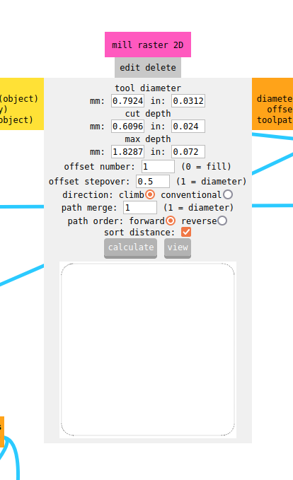
I set the DPI to 1000. I then chose a 0.4mm bit (1/64") for milling. In the file, the areas to be milled out are shown in black, while the areas that remain as the traces are shown in white. You can view the path by clicking on the view button after calculated.
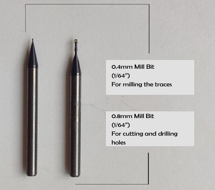
Next I switched on the machine and pressed the view button on the machine control panel and the module moves to its home position. Then, I added the 0.4mm bit on the collet chuck using an Allen key.
For the material, I used FR-1 PCB and cut out a piece of double-sided sticky tape of the same size. After ensuring there was no sticky residue left on the machine bed from previous work, I secured my board to the machine bed with the tape.
From MODs, I adjusted the origin position and clicked on move to origin.
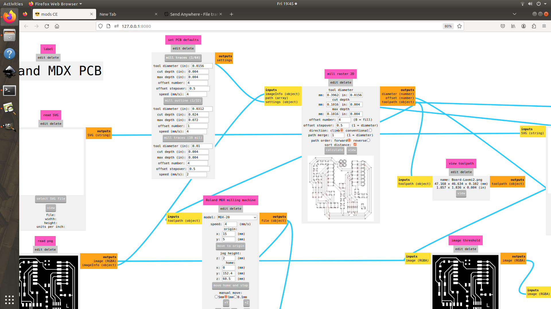
Then, with the help of down button on the machine control panel, I moved the bit module so that the bit gently touch the PCB board.
Click on send file to start the milling process.
Next process was to drill the required holes and to cut out a border for the milled PCB. We have been provided with .png files for the same from Fabcloud. So I imported the files on MODs.
Then, I changed the bit to 0.8mm (1/32") which is suitable for cutting and drilling, and repeated the same process.
Here's the final outcome.
Soldering
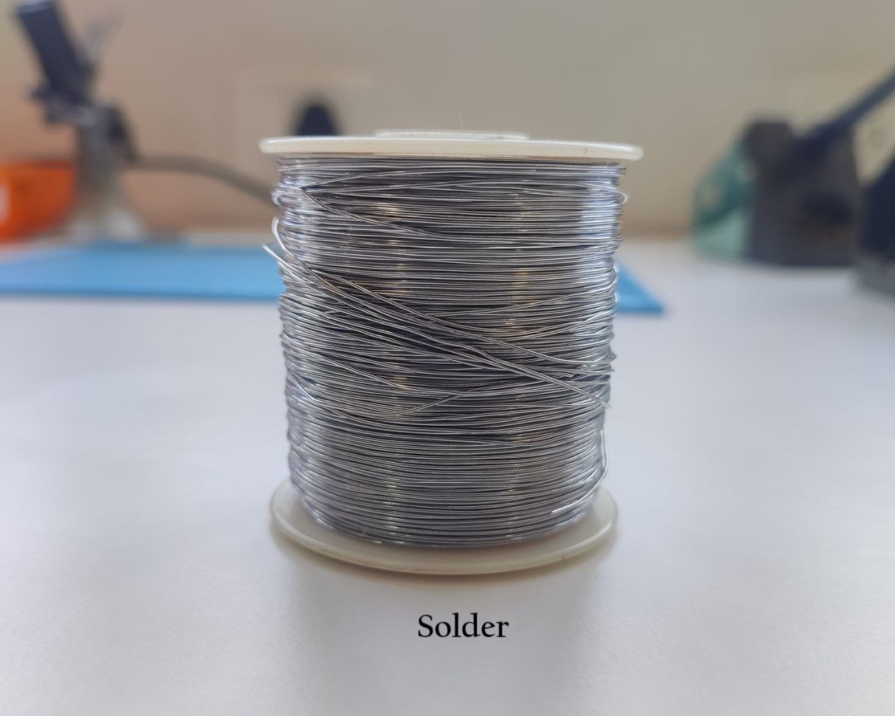
Soldering is a process used to join two or more metal items together by melting and flowing a filler metal (solder) into the joint, the filler metal having a lower melting point than the adjoining metal. It's commonly used in electronics to connect components to circuit boards. The solder typically used in electronics contains tin and lead, although lead-free solders are increasingly common due to health and environmental concerns. In Super Fablab, we use lead-free solders.
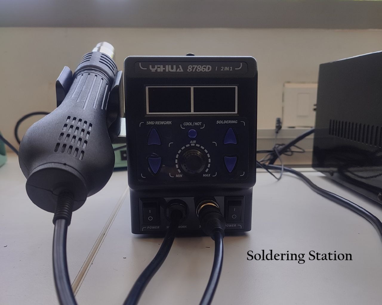
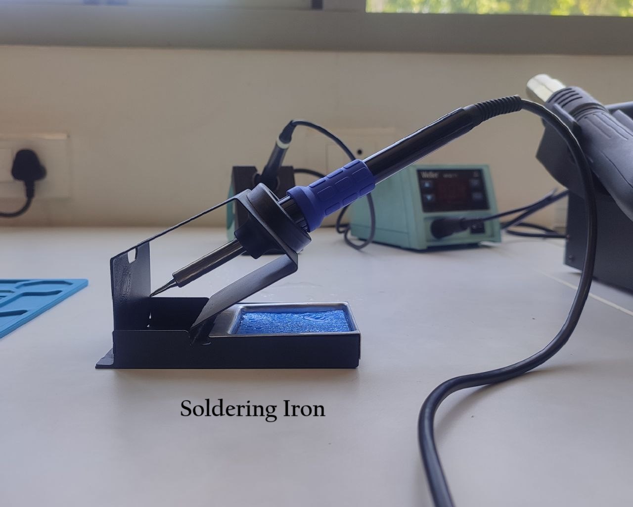
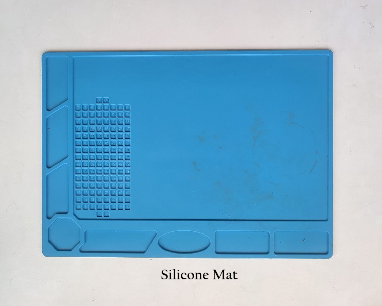
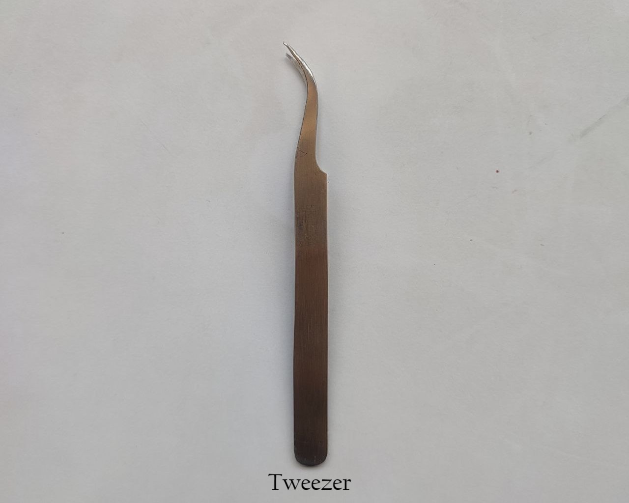
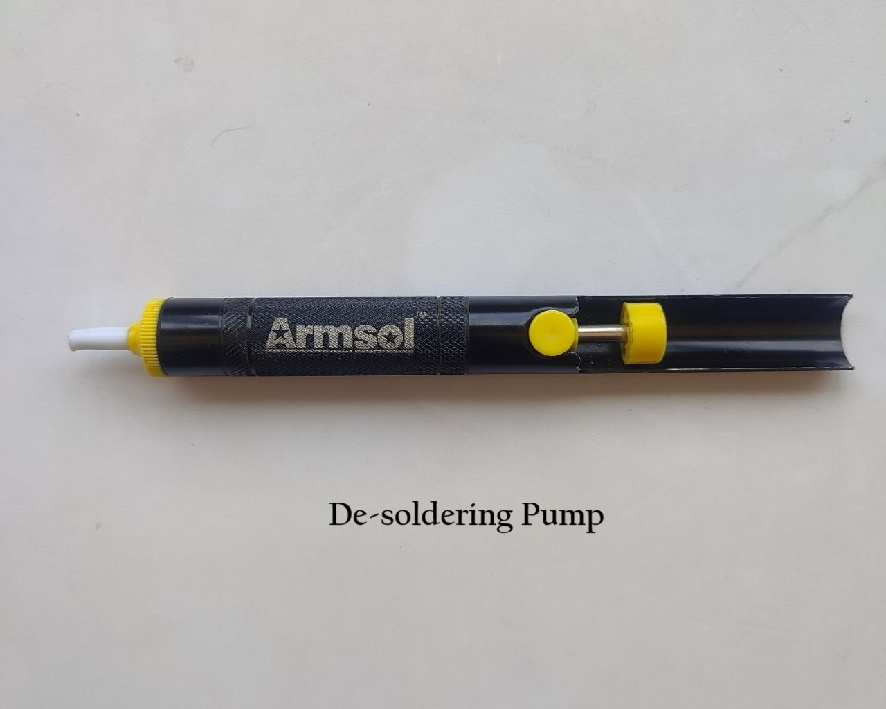
Tools used for Soldering:
Safety Measures for Soldering:
- Ensure adequate ventilation in the soldering area to avoid inhaling fumes from the solder and flux, which can be harmful. Fume extractors (fans) or working near an open window can help.
- Wear mask if you are working in a poorly ventilated space.
- Use tools like tweezers or clamps to hold components in place, keeping your fingers away from the heat.
- Always return the soldering iron to its stand when not in use; never leave it unattended while it's hot.
- Wash your hands after soldering to avoid ingestion of harmful substances.
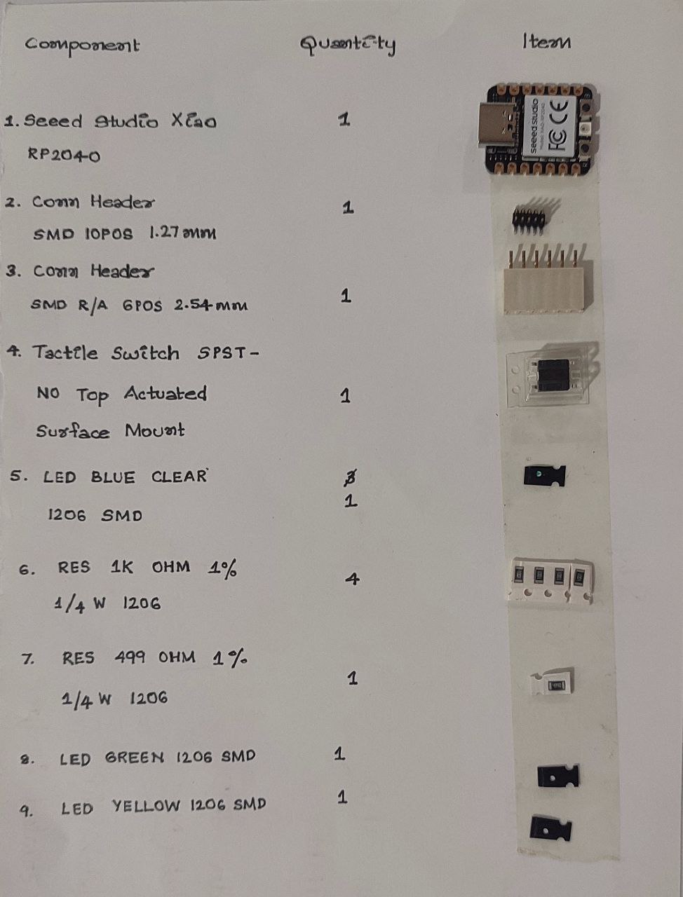
In our Fablab, we have a website to request for components that are part of the inventory. We were given credentials to login and I added the components as per the list to the cart and sent request. Once accepted by the Admin, I gathered all the components.
Then, it was time to solder the components. First, our instructor gave us an idea on soldering station, how to solder and some tips that will help to ease the process.
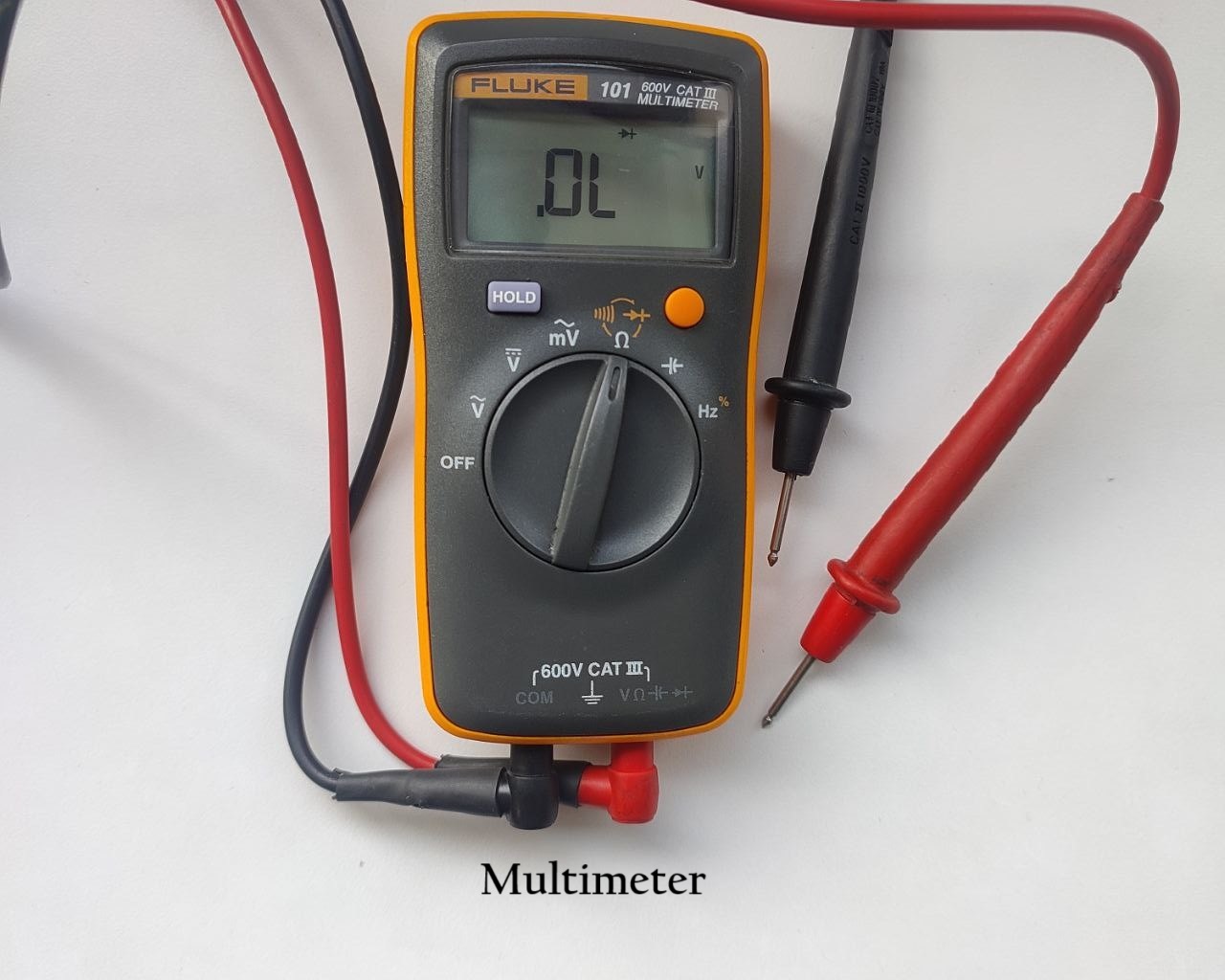
Then, I soldered the components to the board one by one according to the diagram provided below. Here, except for LEDs, none of the other components have polarity concerns, meaning you can solder them in any orientation without worrying about their polarity. However, for LEDs, I used a multimeter to determine their positive and negative terminals to ensure they were aligned correctly.
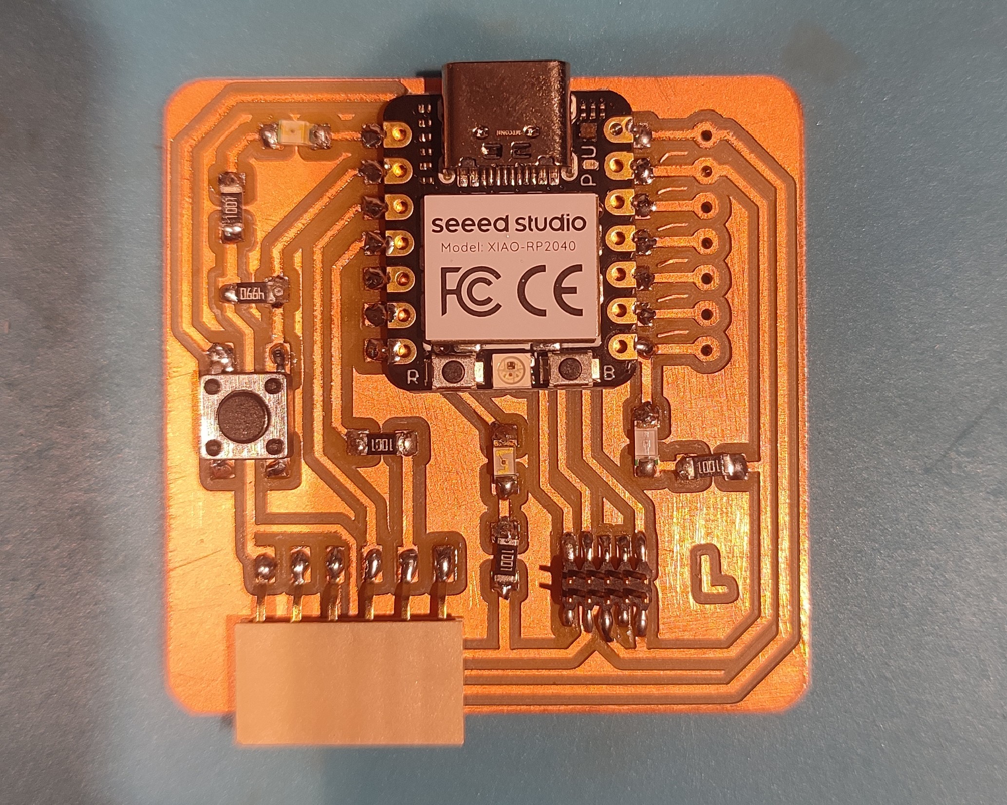
I found the process to be really satisfying. Here's the final outcome:
Coding
After soldering, next step is to check if the board is working and that the soldering process is adequate. For that, I used multimeter to a check the continuity of the each connections. Turns out everything was fine.
I downloaded Arduino IDE 2.3.1 . The Arduino IDE is a free, open-source programming environment used for writing and uploading code to Arduino microcontroller boards. It features a simple, user-friendly interface with a text editor for writing code, a message area for feedback, a console for displaying output, and a toolbar with buttons for common functions.
Designed for both beginners and experienced programmers, it supports C/C++ based coding, offering features like syntax highlighting, auto-completion, and error highlighting to ease the development process. The IDE includes a library manager for adding libraries, a board manager for configuring various Arduino boards, and a serial monitor for real-time communication with the Arduino hardware. It is available for Windows, macOS, and Linux, making it accessible to a wide range of users aiming to develop projects in areas such as robotics, IoT, and beyond.
It was my first time using the software, and I followed a tutorial as well as consulted the Arduino Help Center to resolve any doubts. I posted the errors I encountered during compilation in the Arduino Help Center to find solutions.
Tutorial : This tutorial details the initial setup and configuration of the Arduino IDE to make it compatible with the specific board I am using, the Seeed Studio XIAO RP2040. The board features three LEDs, and I modified an existing code to achieve my goal of making the LEDs blink in a consecutive loop.Once I downloaded Arduino IDE, Select File > Preference. In the option for Additional Board Manager URLS, copy and paste the below URL and click OK.
https://github.com/earlephilhower/arduino-pico/releases/download/global/package_rp2040_index.json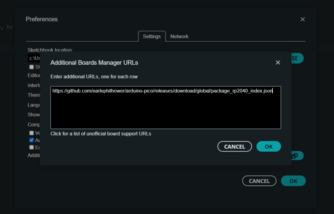
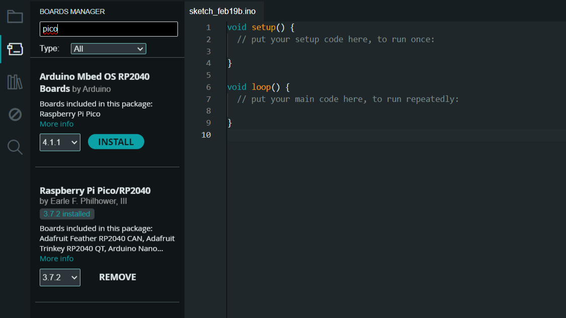
Then, open Tools > Board > Board Manager. Type "pico" on the search bar and download Raspberry Pi Pico RP2040.
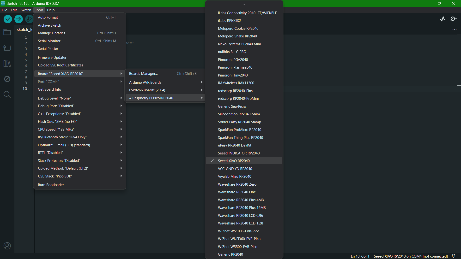
Once it is installed. Select Tools and follow the steps as given to select the board.
Then, I modified the code to sequentially light the LEDs.
Here's the modified code:
        void setup()
        {
          pinMode(26, OUTPUT);
          pinMode(0, OUTPUT);
          pinMode(1, OUTPUT);
        }
        // HIGH and LOW are the voltage levels
        void loop()
        {
          digitalWrite(26, HIGH);
          delay(500);
          digitalWrite(26, LOW);
          delay(500);
          digitalWrite(0, HIGH);
          delay(500);
          digitalWrite(0, LOW);
          delay(500);
          digitalWrite(1, HIGH);
          delay(500);
          digitalWrite(1, LOW);
          delay(500);
        }
Once the code was ready, I uploaded the code onto the PCB and the LEDs started blinking sequentially.
Reflow Soldering
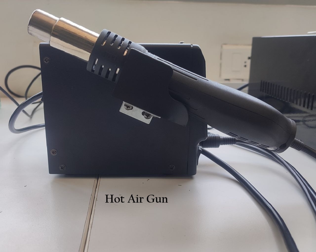
As our weekly assignements were completed, our instructor, Saheen suggested we try reflow soldering. Reflow soldering is a process used to attach electronic components to printed circuit boards (PCBs) with surface mount technology (SMT). The process involves applying solder paste (a mixture of solder and flux) to the board, placing components on top, and then heating the assembly in a reflow oven or with a hot air gun. The heat causes the solder paste to melt (reflow), forming solder joints that electrically and mechanically connect the components to the board once cooled.
In our fablab, we have the provision to use both hot oven and hot air gun.
- 5.12k Ohm Resistors: It limits the amount of current that flows throught he circuit with respect to power. For our work, we used 2 resistors.
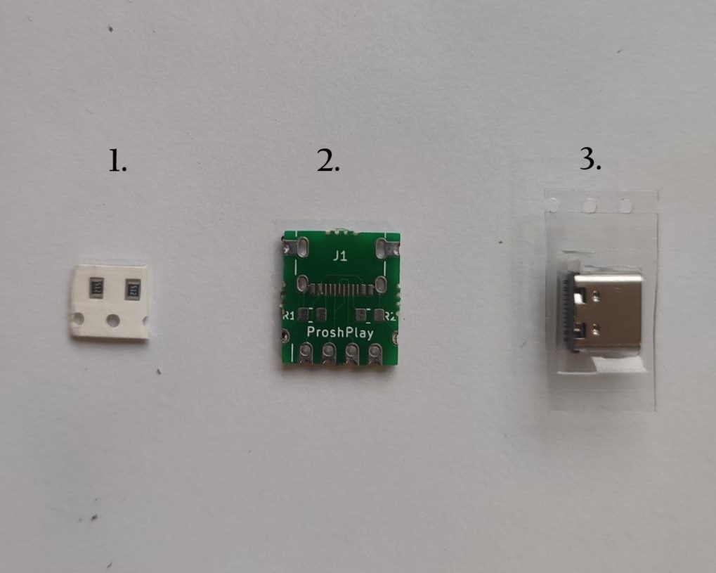
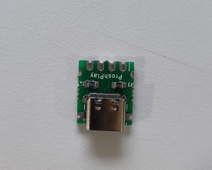
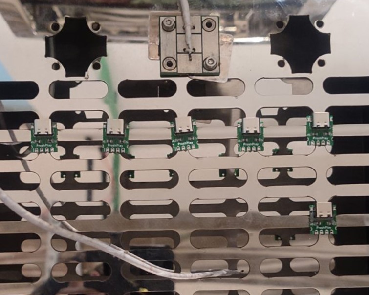
- Breakout Board: The breakout board is designed by one of our instructor, Saheen. It has 4 -pins, namely, positive, negative, D+ and D-. Two of these, D+ and D-, form a twisted pair responsible for carrying a differential data signal, as well as some single-ended signal states.
- Type C connector: It is a 16 pin type C connector.
Tools & Equipments used:
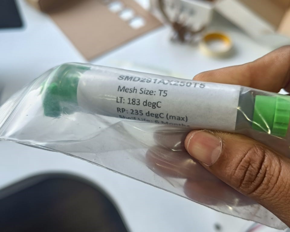
• Solder Paste: SMD291AX250T5 (max. temp: 235°C)
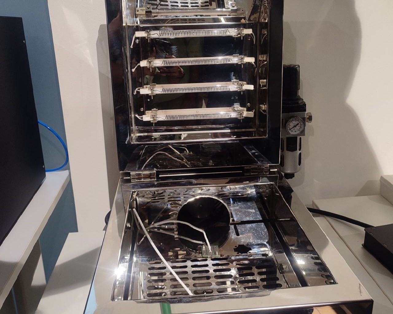
• Hot Oven: PlacerBot-Reflow Oven
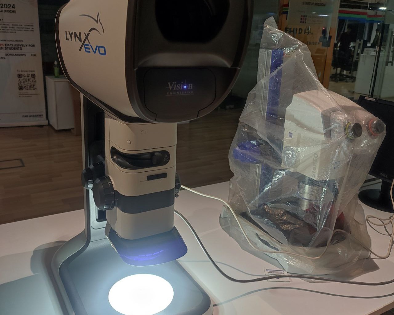
• Microscope: Lynx Evo Microscope
Stencil was made in order to transfer the solder paste to the breakout board. We applied the paste onto the board by smearing the paste over the stencil using a card.
On top of the paste, I placed all the components that has to be soldered on their respective positions. The below image shows the components in their own positions before reflow.
Next step is to place the board in the oven.
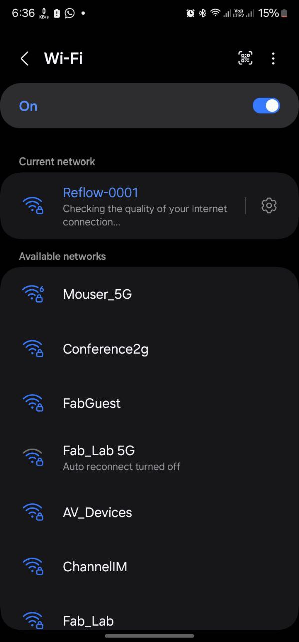
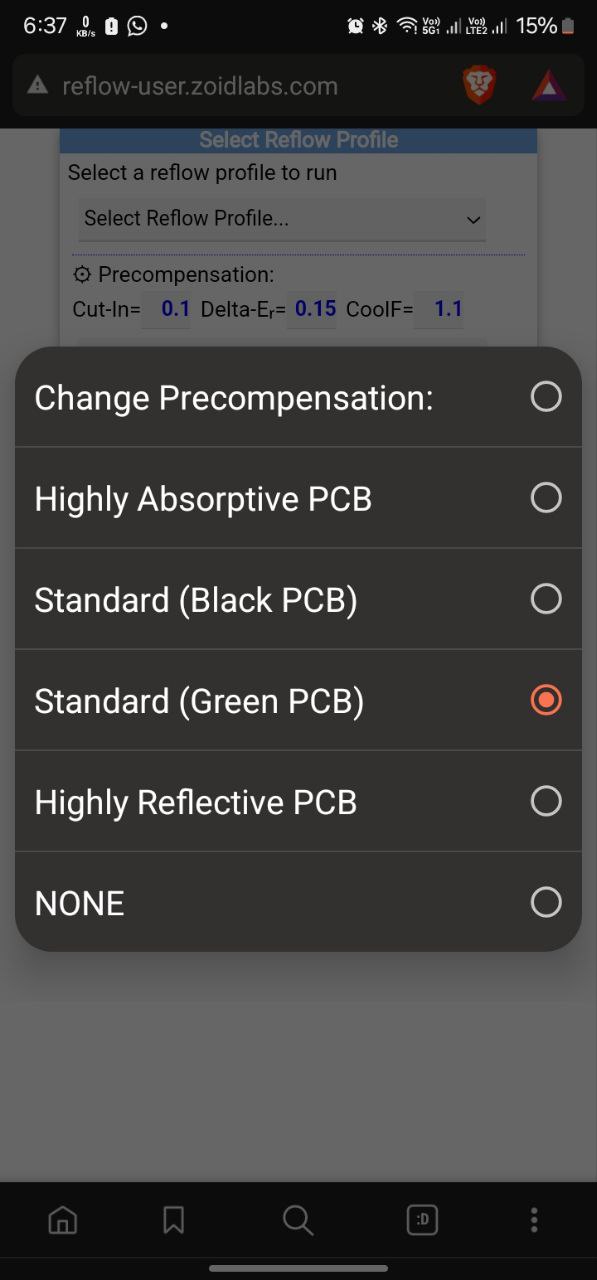
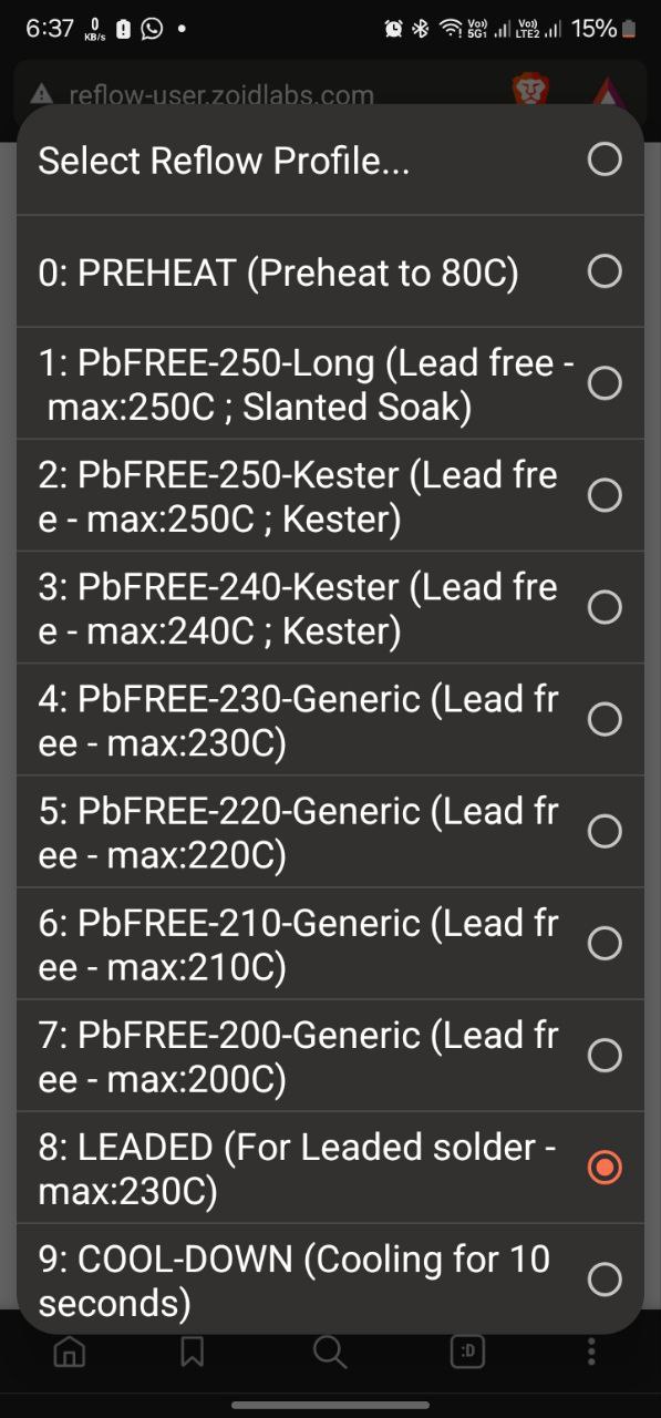
To control the oven we have a software. In order to do that, first we have to connect to the network as below:
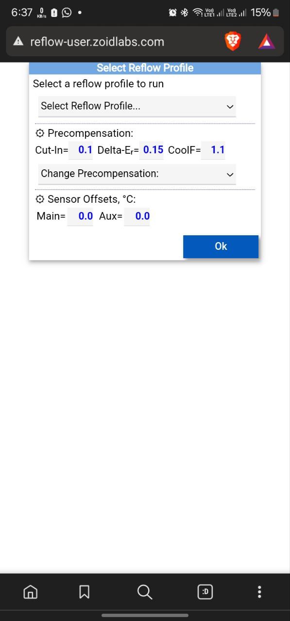
Once connected, open the link on browser:https://reflow-user.zoidlabs.com/. Then we selected the parameters as per our work.
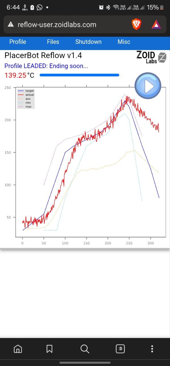
While the process of reflow soldering happens, we can view the Reflow Soldering Temperature Graph (Temp. vs. Time).
Preheat Zone:
• Purpose: Evaporate any remaining solvents or moisture from the PCB and components.
• Temperature Range: 100°C to 150°C.
• Duration: 60 to 120 seconds.
Temperature Ramp-Up (Pre-reflow):
• Purpose: Gradual heating to avoid thermal shock to the components.
• Temperature Range: 1 to 3°C/second.
• Duration: Up to the liquidus temperature.
Soak Zone (Temperature Soak):
• Purpose: Maintain the temperature close to the liquidus for a specific duration.
• Temperature Range: Close to the solder paste's liquidus temperature.
• Duration: 60 to 180 seconds.
Reflow (Peak) Zone:
• Purpose: Achieve complete solder melting.
• Temperature Range: Above the solder paste's liquidus, typically around 220°C to 260°C.
• Duration: 10 to 120 seconds.
Cooling Zone:
• Purpose: Gradual cooling to solidify the solder joints.
• Temperature Range: Controlled cooling, typically 2 to 3°C/second.
• Duration: Until the PCB reaches a safe handling temperature.
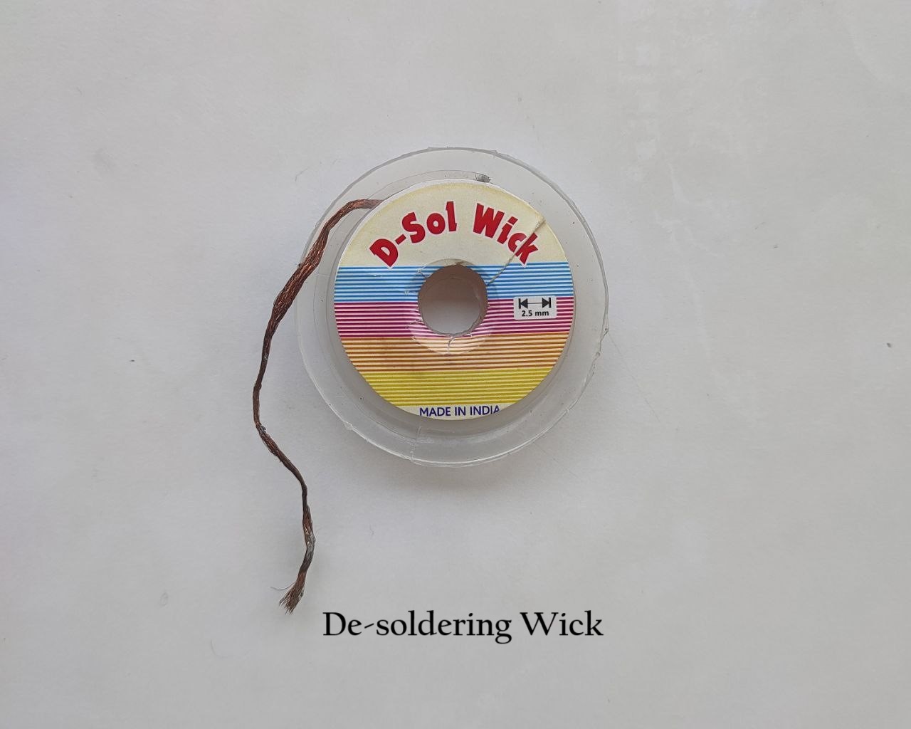
Once completed, we took out the board and inspected it under the microscope. Turns out it was shot. It had three points were the pins of the Type-C connector were joined. So, with the help of de-soldering wick and soldering iron, I fixed my board.
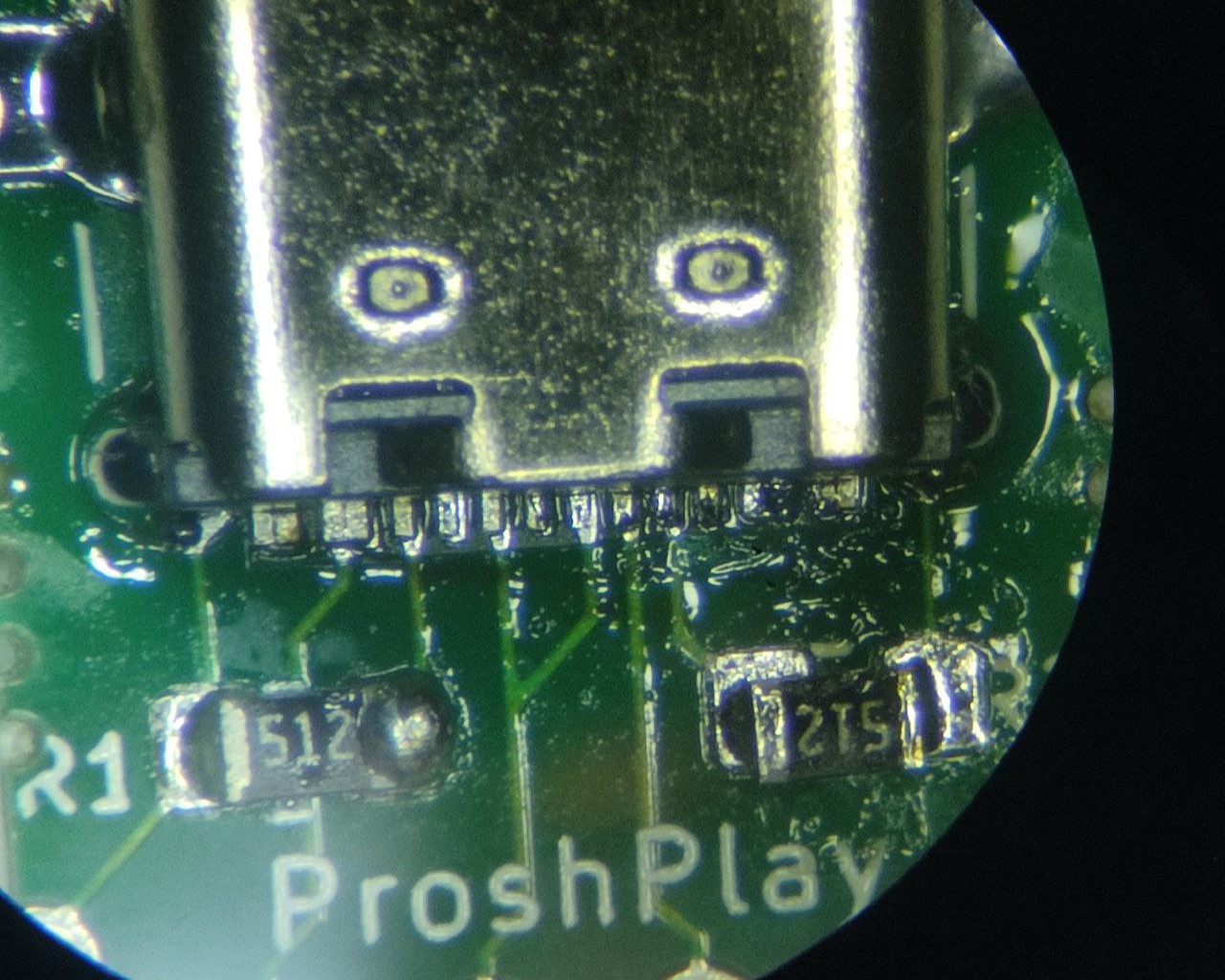
Here's the final product:
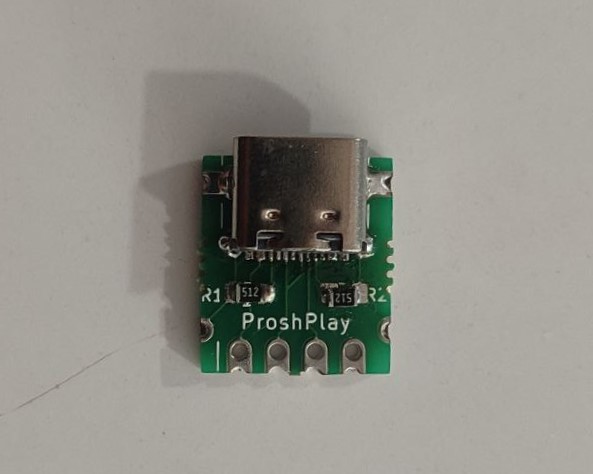
In order to confirm all connections are right, I checked its voltage using multimeter and fortunately it was working.
.jpg)
This week was pretty intersting as it was my first proper experience in milling a PCB and soldering. Fortunately, I didn't come across any issues except when the breakout board was shot which was then corrected.
Download Files
Quentorres (.png file)
Quentorres Interior (.png file)
Quentorres Drills (.png file)
Customized Board (.png file)