-copy.jpg)
Wildcard Week
The assignment for this week:
- Design and produce something with a digital process (incorporating computer-aided design and manufacturing) not covered in another assignment, documenting the requirements that your assignment meets, and including everything necessary to reproduce it.
Adventuring through the Wildcard week
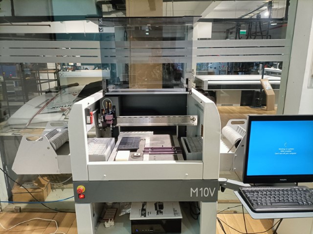
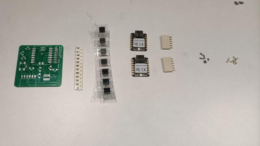
Through the course, soldering was not my piece of cake. Though I enjoyed doing it at times, I would spend relatively a long time chasing the resistors and capacitors on the silicon pad with the tweezers or trying to place the LEDs in the right position based on the polarity. Somehow, soldering was taking time too, either the lead would be of too little quantity such that the connections were not properly made or the quantity would be too much such that it would flow to the nearby pad. When I heard about the M10V SMD pick and place , I really wanted to try out the machine. The Wildcard week was perfect for experimenting this. Though the real advantage is when you are placing components on PCBs of large quantities, I enjoyed learning about this machine with the help of my instructor, Saheen. It is all about teaching the machine once of how to identify the components and then showing it the exact location and position for it. The machine has an option to dispense soldering paste at the locations you want too. Once the 'teaching' is over, the machine is an exceptionally good student, the rest is cakewalk! It was quite fascinationg watching the speed and accuracy at which the components are placed.About the MV10 SMD Pick and Place
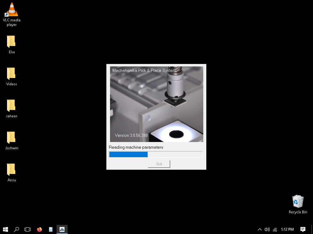
The M10V SMD pick and place machine is a piece of equipment commonly used in electronics manufacturing for the assembly of surface mount devices (SMDs) onto printed circuit boards (PCBs). Its features and functions:Overview of the process involved
How a Pick and Place Machine Helps with PCB Assembly?
A pick and place machine plays a crucial role in automating the placement of electronic components onto the PCB, which is a critical step in the PCB assembly process. It helps with PCB assembly in the following ways:Automated Component Placement : A pick and place machine automates picking up electronic components, such as resistors, capacitors, integrated circuits, and other SMDs, from their reels or trays. It precisely places these components onto the designated locations on the PCB based on the coordinates provided by the PCB design.
High Precision and Speed: Pick and place machines offer high precision in component placement, ensuring each component is accurately positioned on the PCB according to the design specifications. These machines can work at high speeds, significantly improving the efficiency of the assembly process compared to manual placement.
Increased Production Throughput: Automation with pick and place machines enhances production throughput, allowing for the rapid assembly of PCBs in large quantities. Faster assembly contributes to quicker turnaround times for manufacturing, reducing overall production time and costs.
Component Variety and Complexity Pick and place machines are versatile and can handle various component sizes, shapes, and types.
Reduced Human Error Automation reduces the risk of human error associated with manual component placement. Pick and place machines operate with precision and consistency, minimizing the chances of misplacements or defects.
Improved Quality and Consistency Automated component placement results in improved quality and consistency across the production line. This consistency is crucial for meeting electronic device performance and reliability standards.
Advanced Vision Systems Many machines have advanced vision systems that can identify fiducial marks on the PCB, ensuring accurate component alignment. Vision systems also assist in detecting and correcting placement errors.
Assembly Flexibility Pick and place machines offer flexibility in production by allowing quick changeovers between different PCB designs.
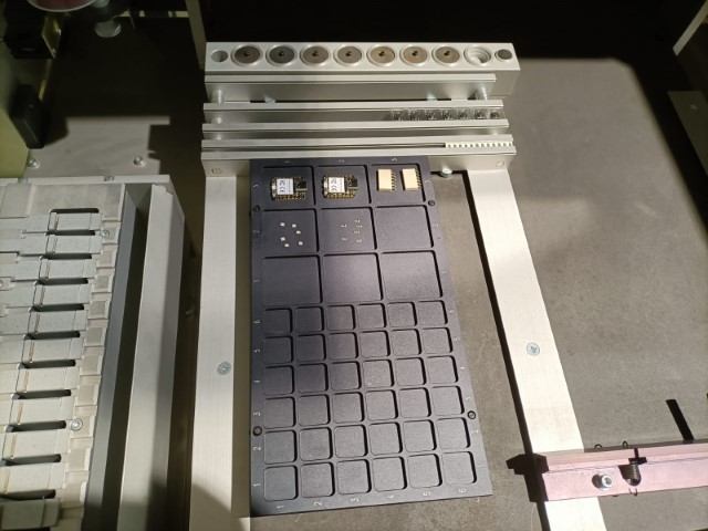
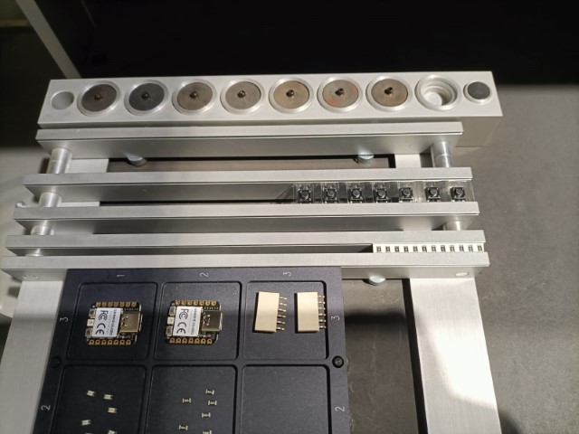
Machine overview
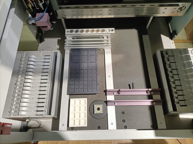
The tape-on-Reel feeders are on the two sides of the machine as shown. They are similar to standard tape feeders but designed to handle larger reels of tape, allowing for longer runs without reloading.
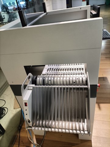
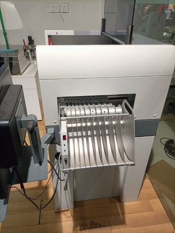
Tray feeders are used for very small or delicate components. Components are arranged in a grid, which ensures they remain in place and are easy to pick.
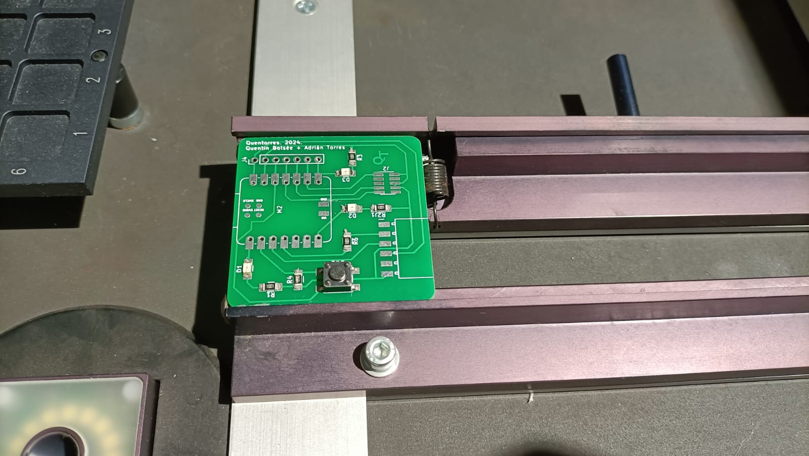
The machine has feeders specifically designed to handle short strips of tape. These feeders can be loaded with the cut tape and feed the components. I have placed the switch and 1K resistors in the tape feeders.
Setting up the machine
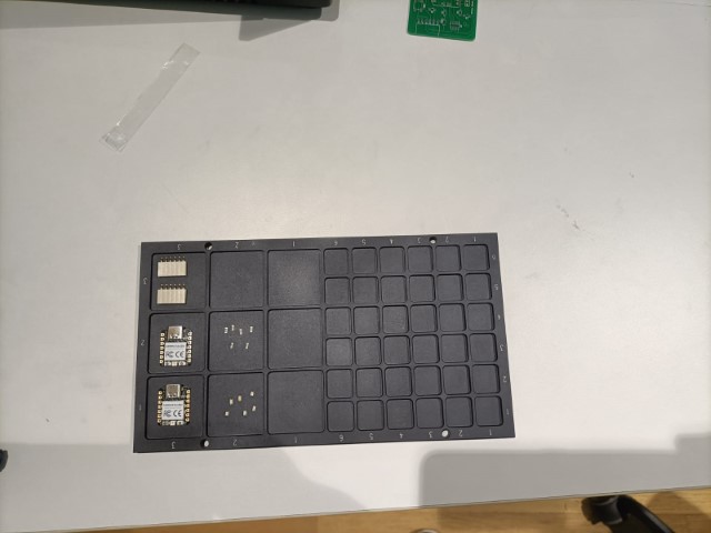
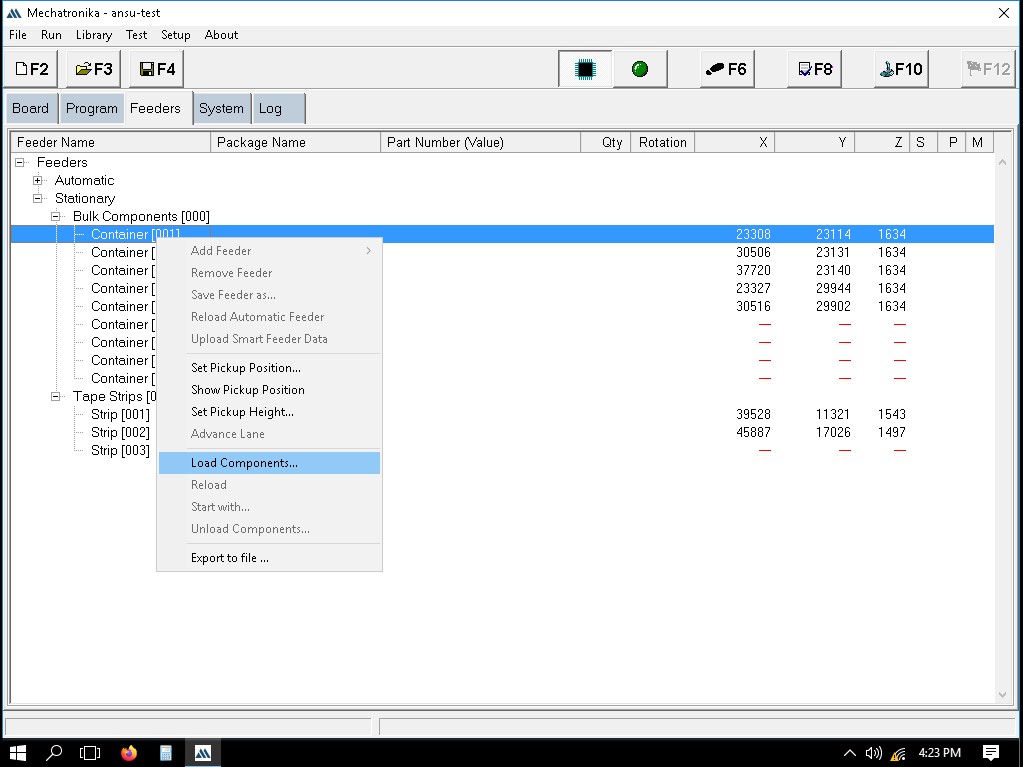
Setting up Feeders
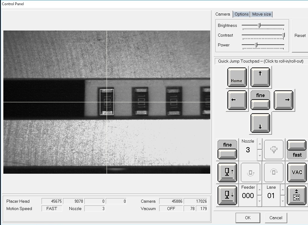
Click on the 'Feeder' tab as shown below: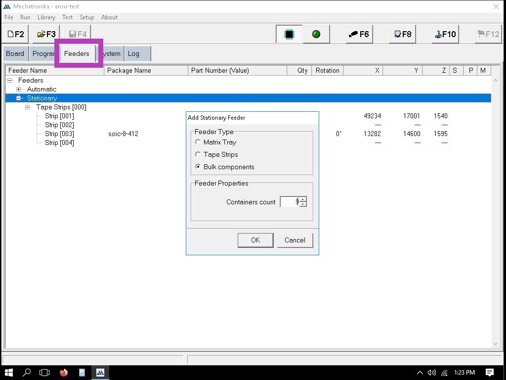
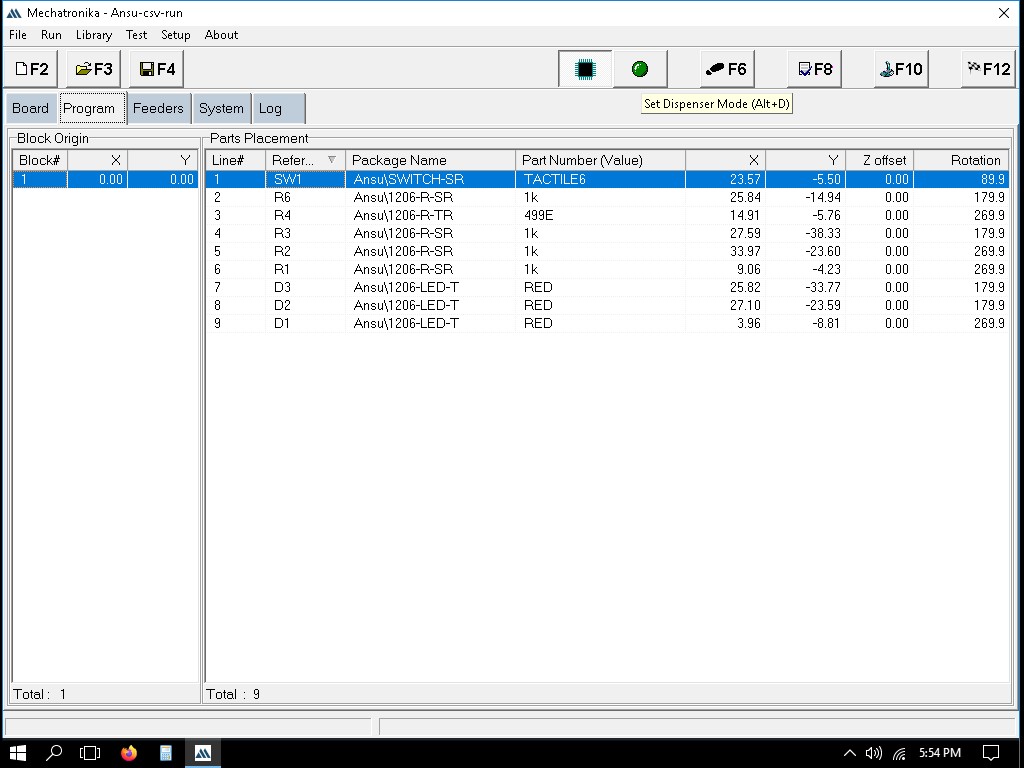
Here, I have added 9 containers and 3 strips.
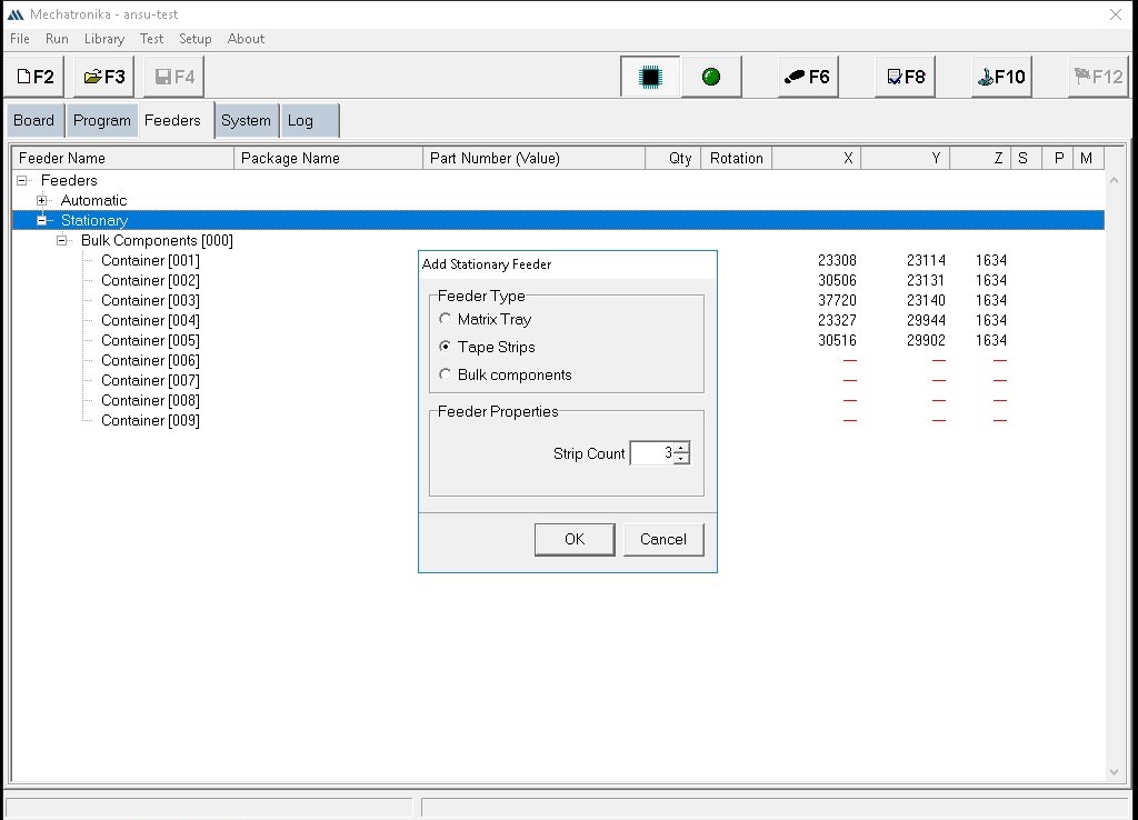
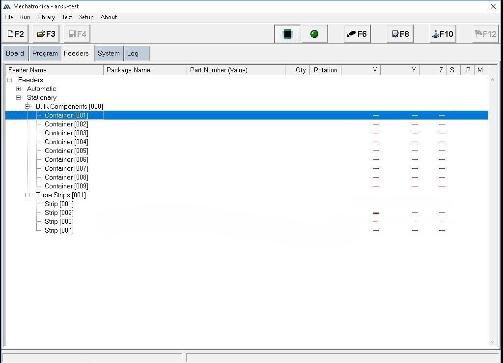
Here, all the containers and strips have been added.
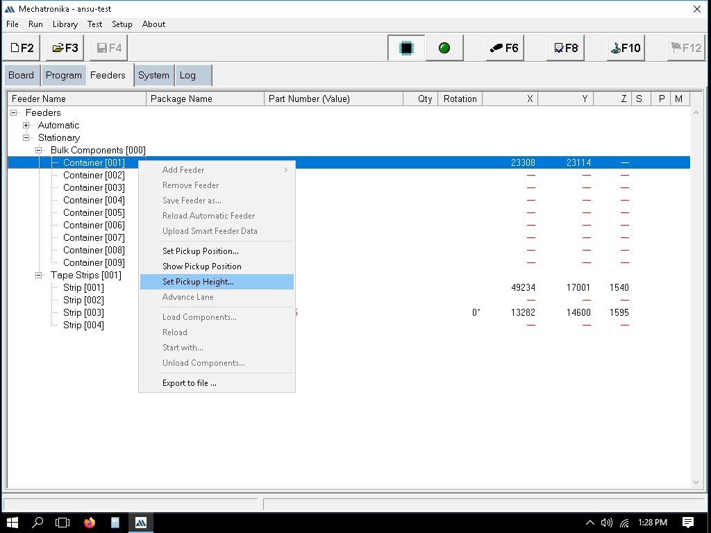
Right click each feeder and click 'Set Pickup Position'.In the new popup window choose either manually type in the position of the tray or teach the machine by selecting Top Left Coordinate/Bottom Right Coordinate of the container.
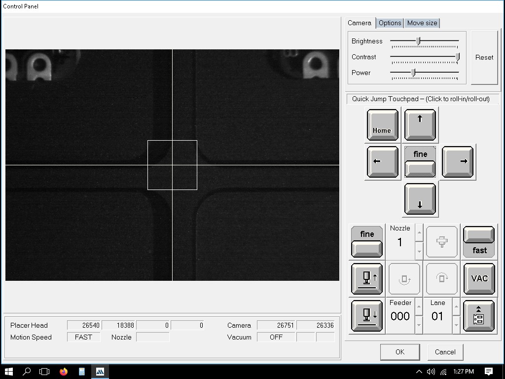
Right click on the container and set height by focusing the camera in an empty container.
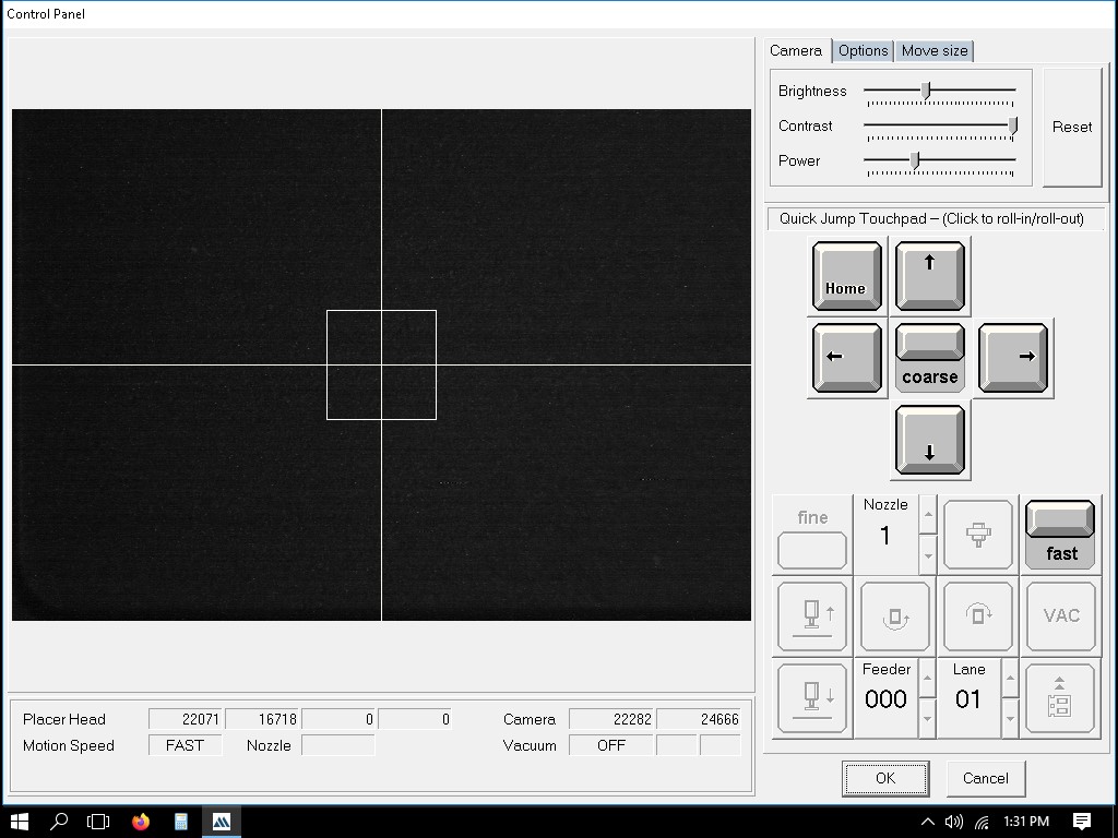
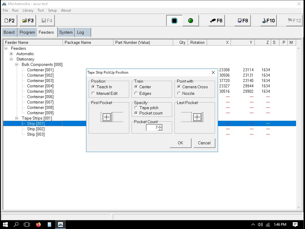
To setup the strips we can show the first and last component and the number of pockets.
Once all the container and strips details are given, we should assign the components to the containers and strips that has been taught now.
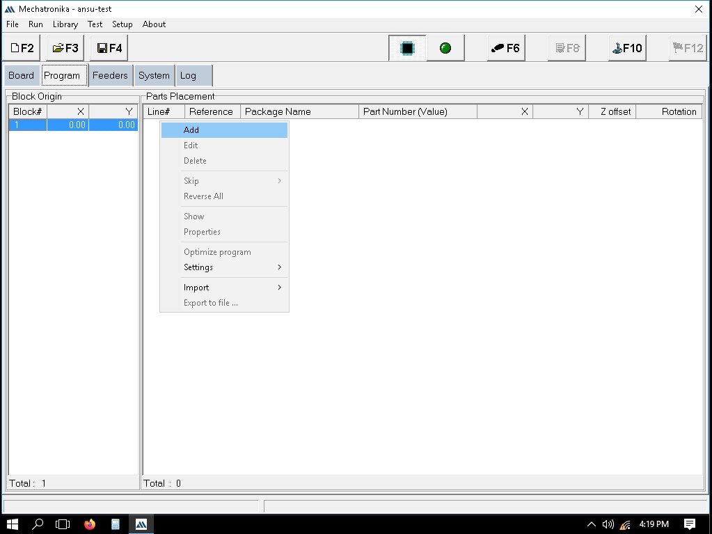
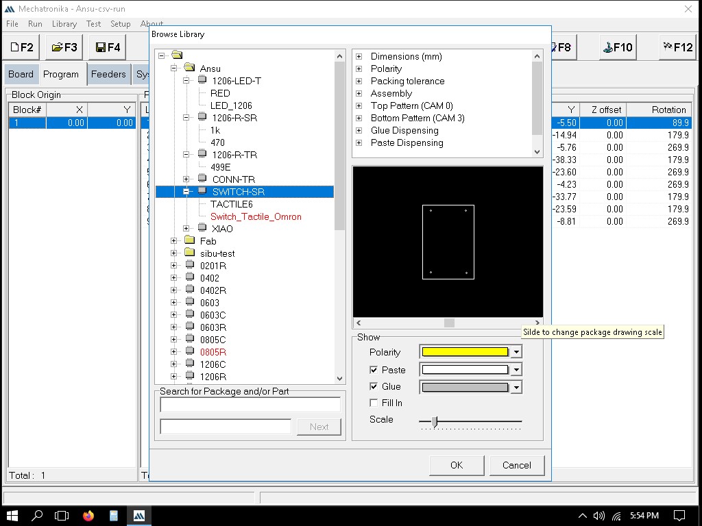
Adding a new part/component
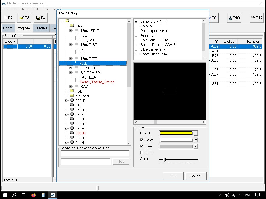
When adding a new SMD component, we first go to "Browse Library," right-click on the file location, and select "New" followed by "Package." Enter the name of the new package in the Package window and click "OK."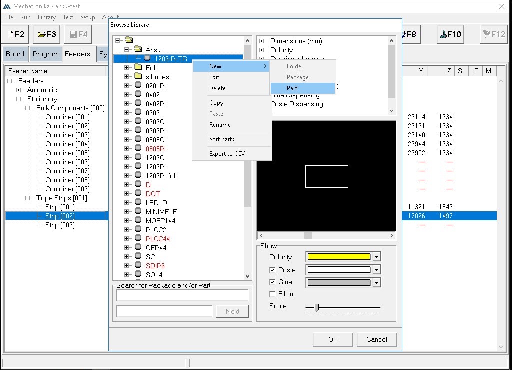
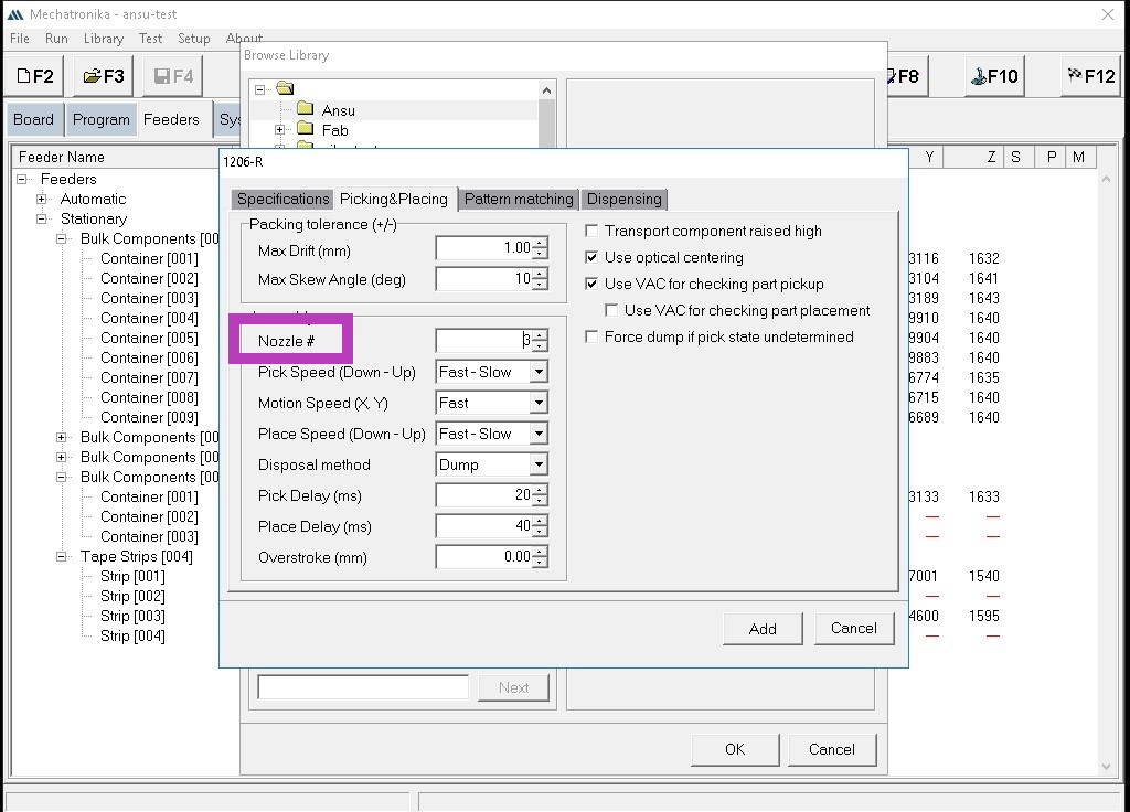
In the window that pops up after creating the new package, the following sessions can be seen:
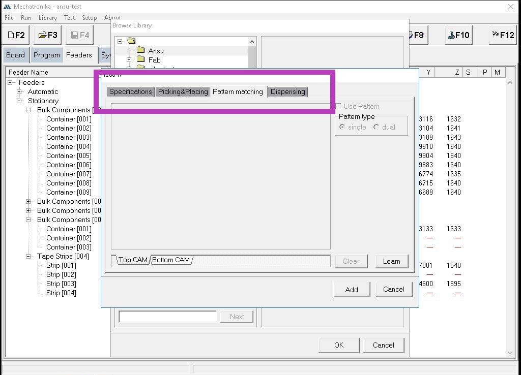
In the 'Specifications' section, we can teach in each component using the look -up and look-down cameras.
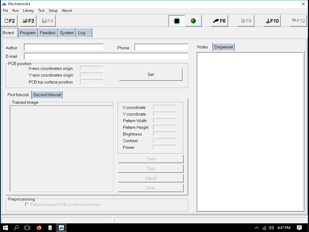
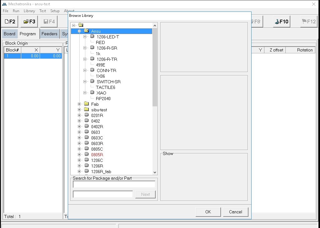
Setting the pcb
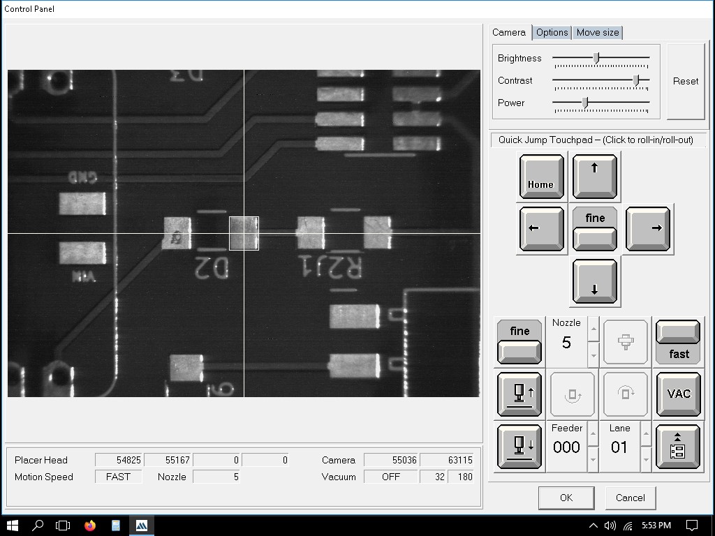
We should teach in the co-ordinates of the PCB.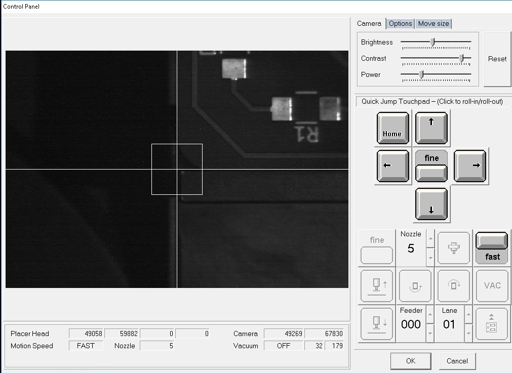
Here, you should show the surface of the PCB.
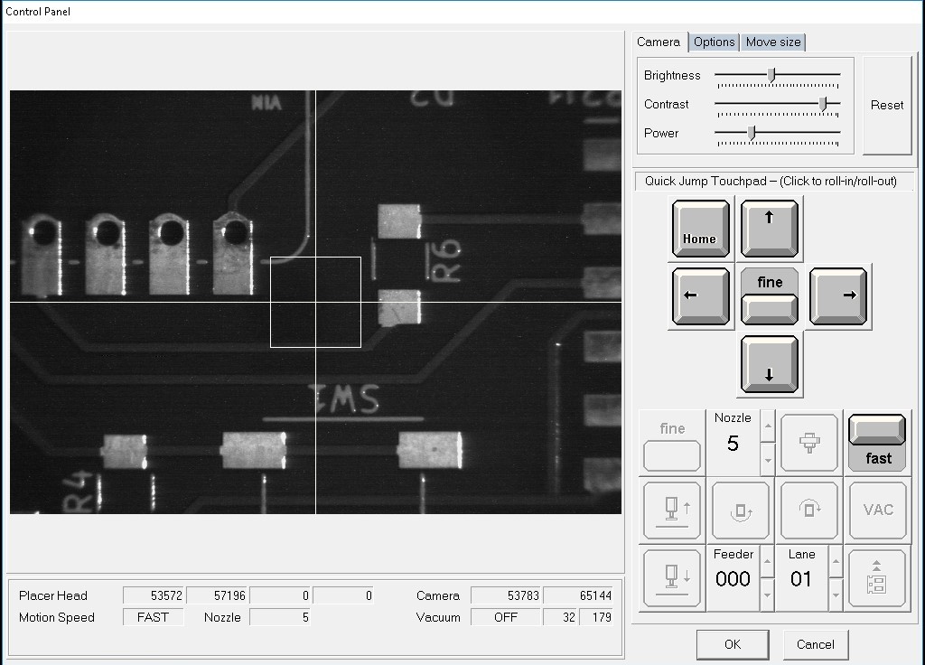
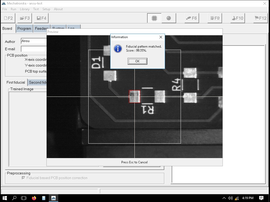
Next, the fiducials which act as refernces for the board.
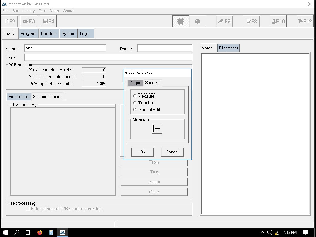
This is the first fiducial point.
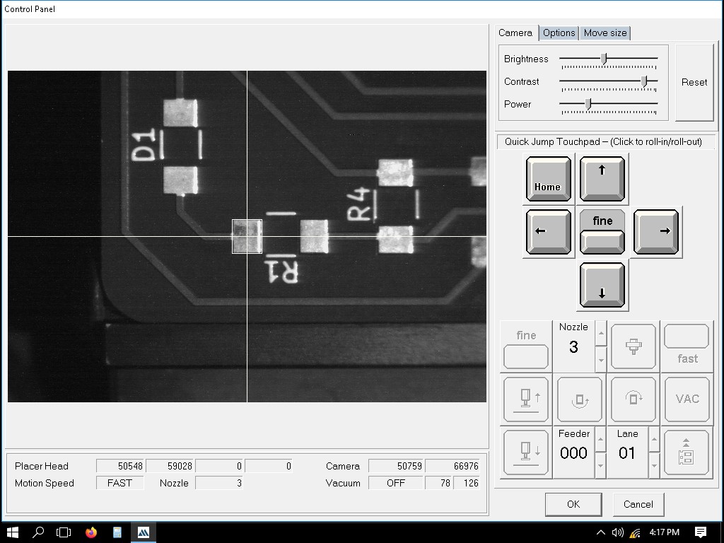
Here, it is being trained.
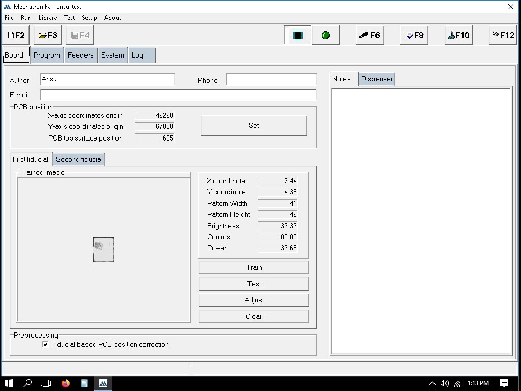
Here, the point is confirmed.
This is the second fiducial point.
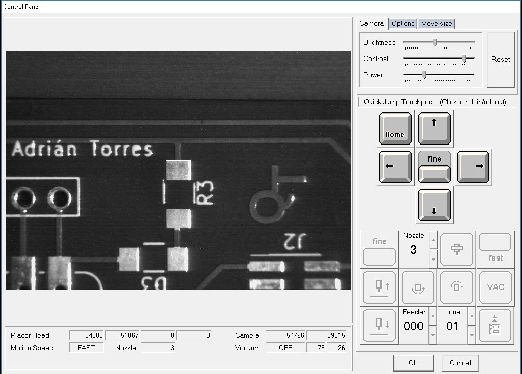
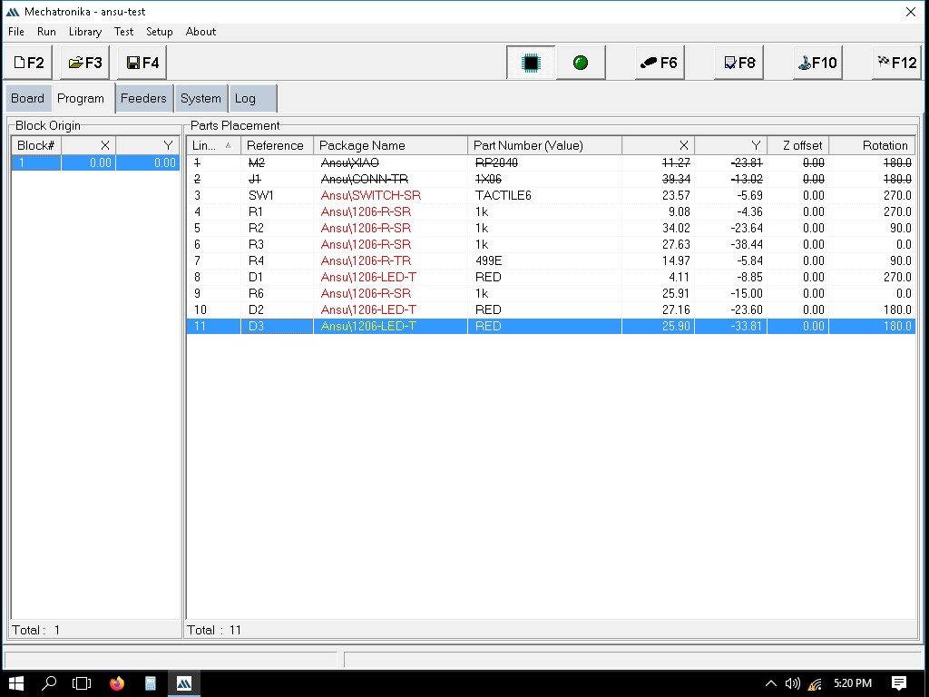
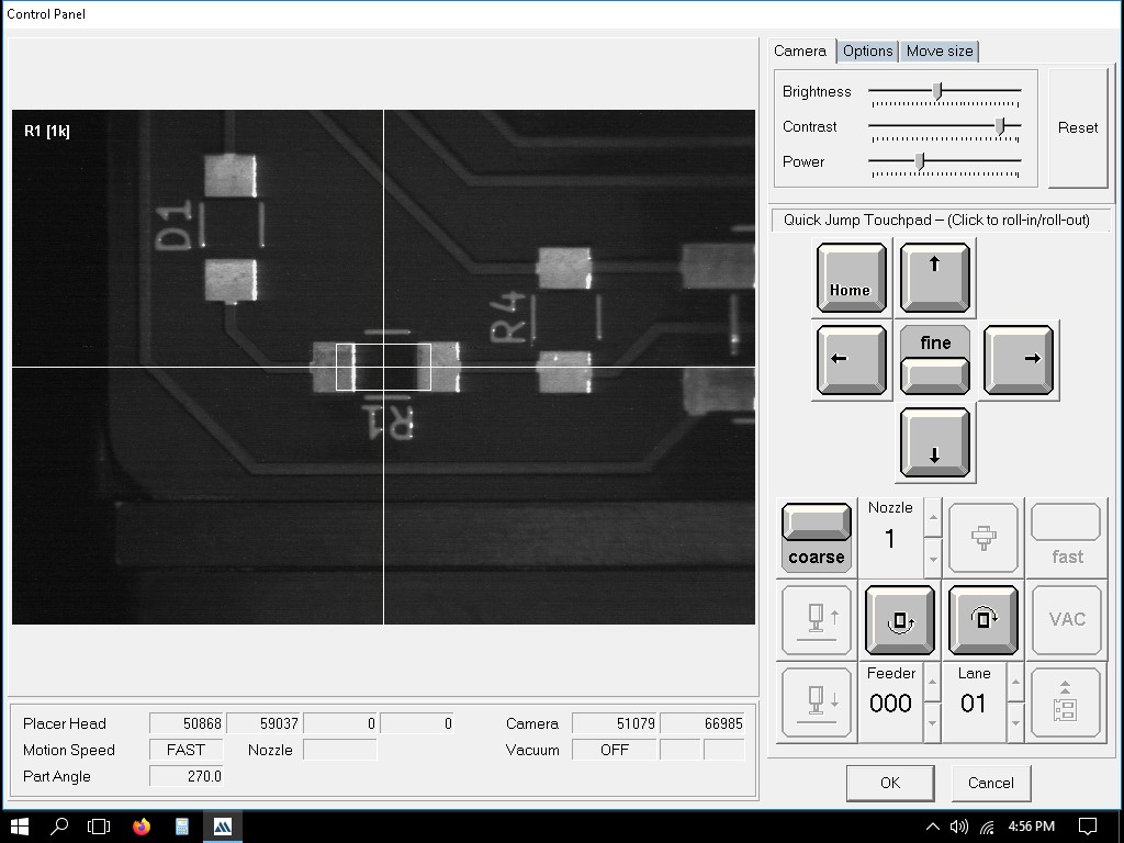
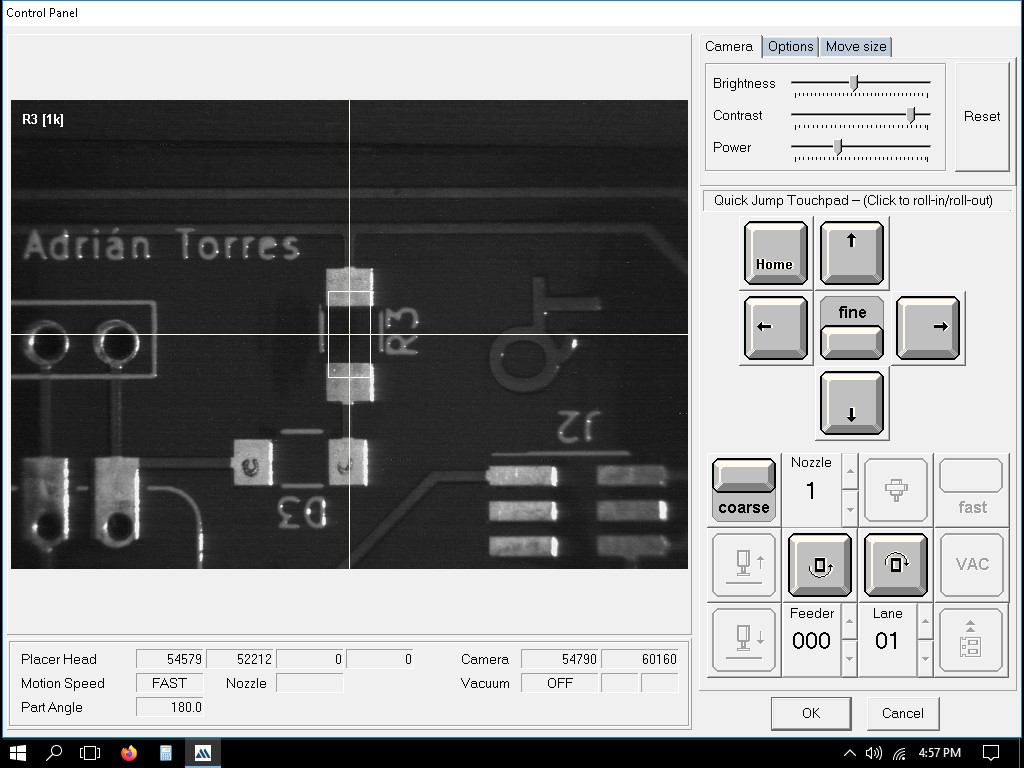
Program the machine
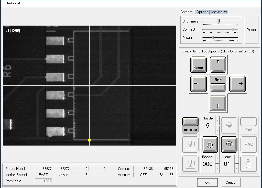
This is for adding the header.
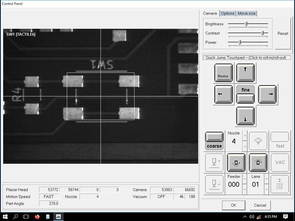
This is for adding the switch.
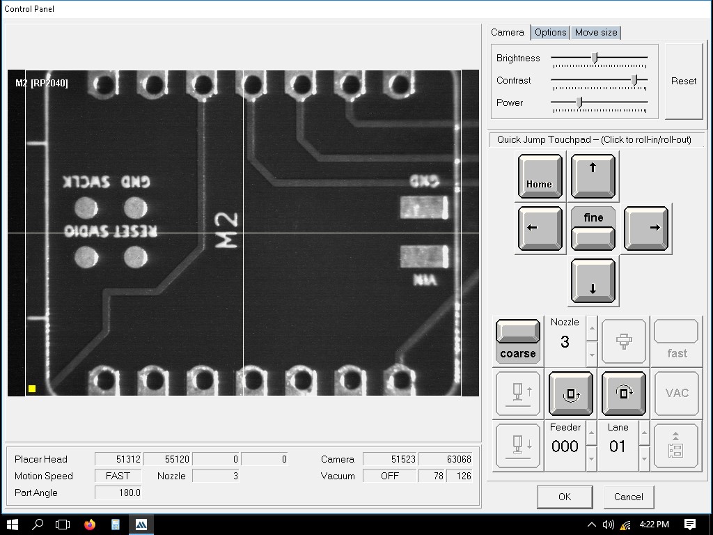
This is for adding the Xiao RP2040.
The Xiao and connector were not picked initially. However, when I changed the nozzle number to 5 and 4 respectively, they were picked. After taking it to the look-up camera it didnt place it but threw it in the collector tray for failed components. Here, the video shows the Xiao RP2040 being picked up.
This is a video showing two failed attempts.
Here, is the video of picking the Conn Header but failing to place it but throwing it into the collector tray.
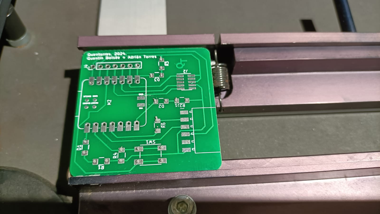
Placing the remaining components as shown below. Though, it tossed few components in the collector tray since it would have failed the image comparison test.
Successfully placed remaining components
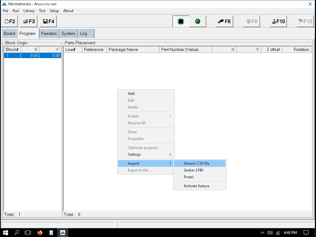
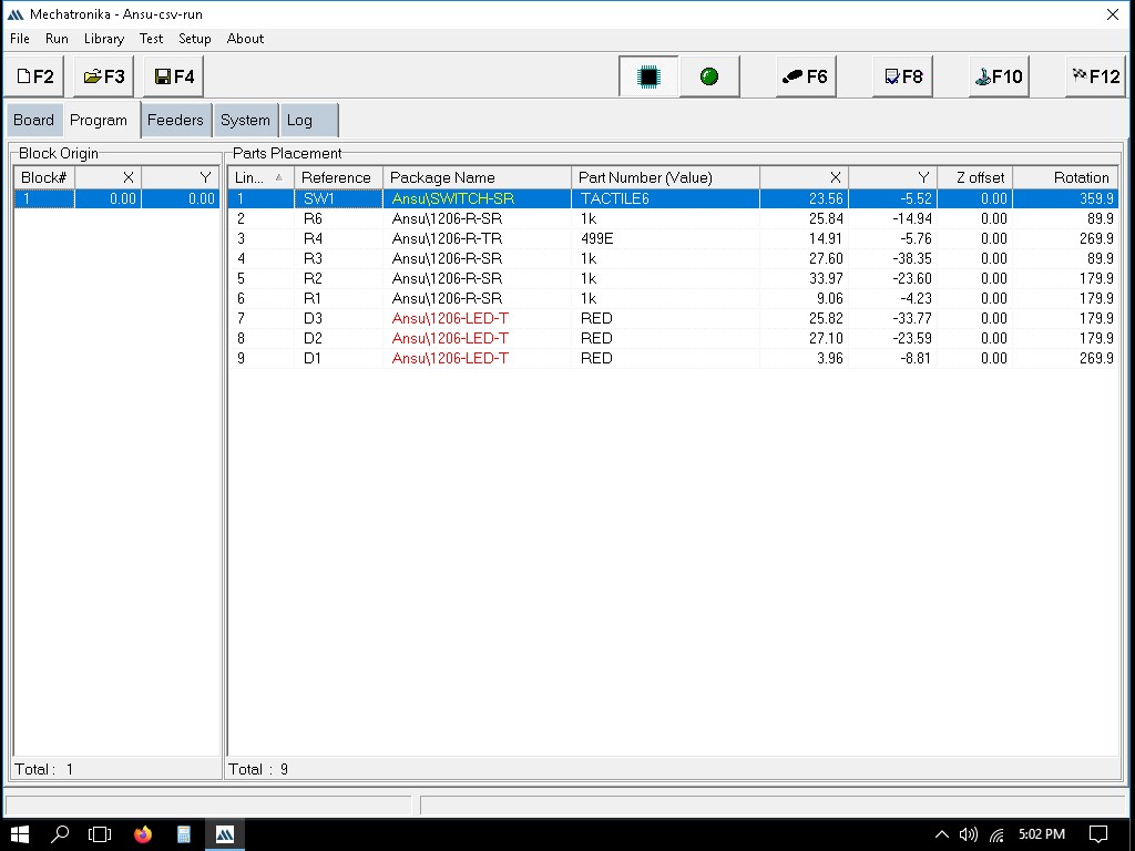
Exporting the file as .csv
We can import the Quentorres file from here - Version 1(v1).png)
.png)
.png)
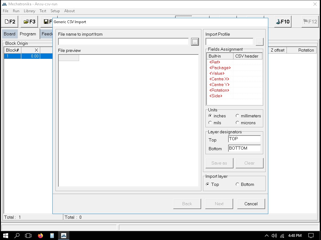
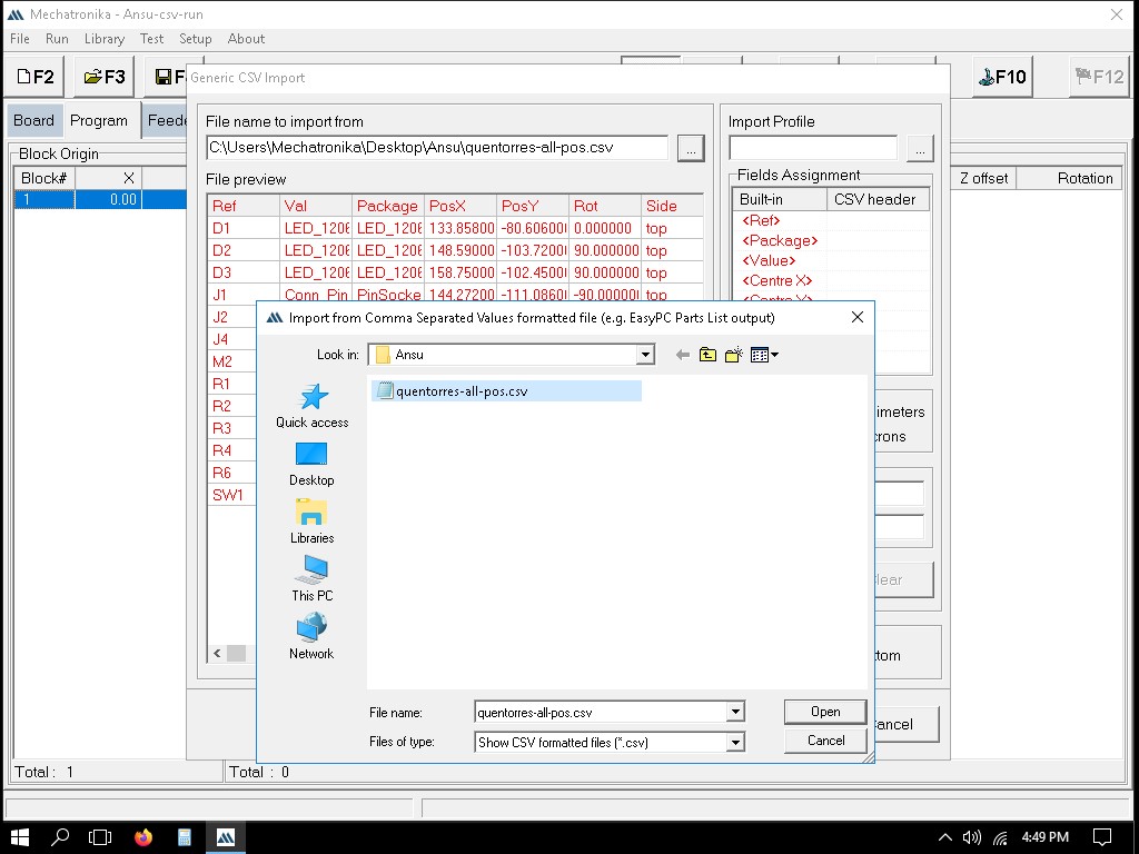
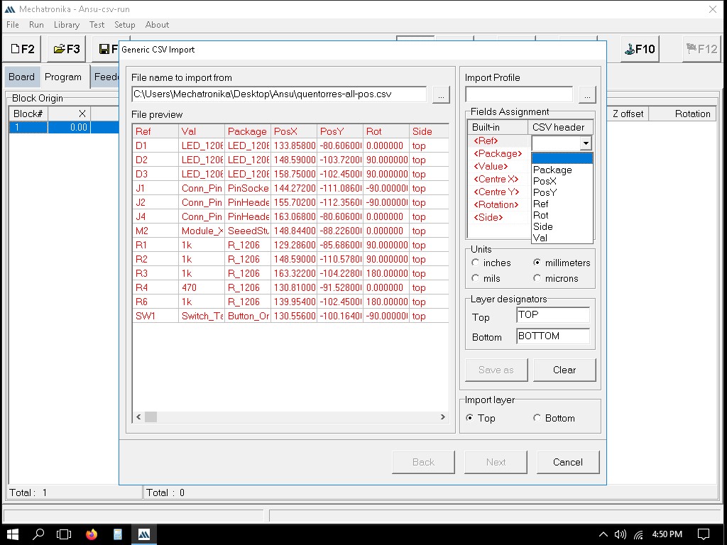
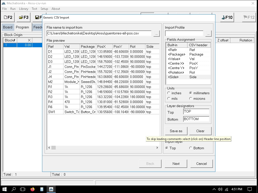
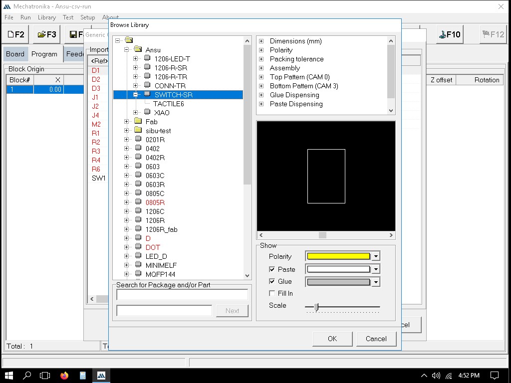
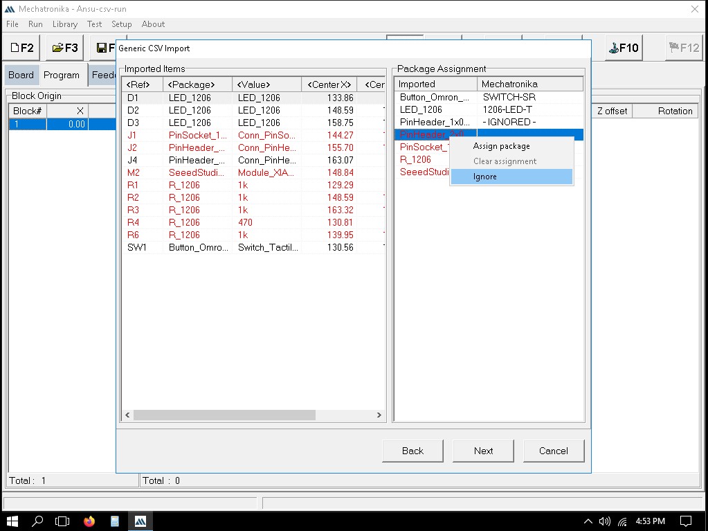
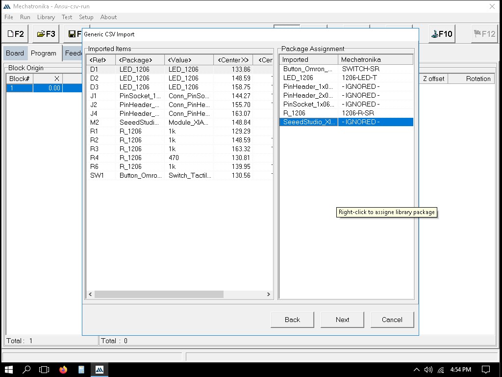
Importing the file to Mechatronika
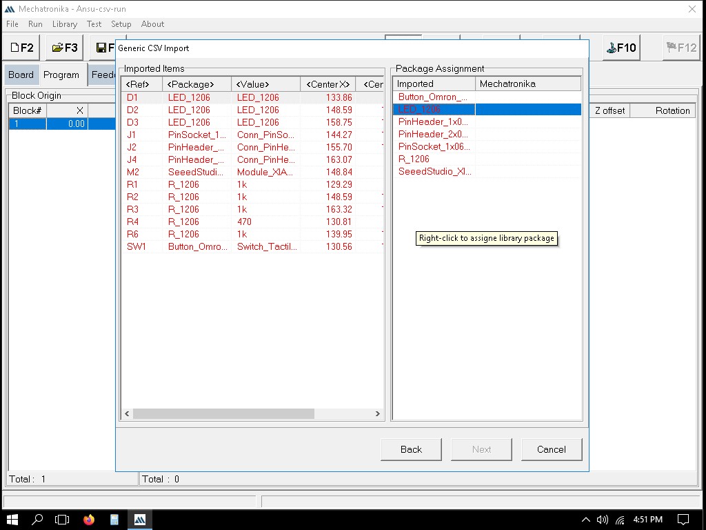
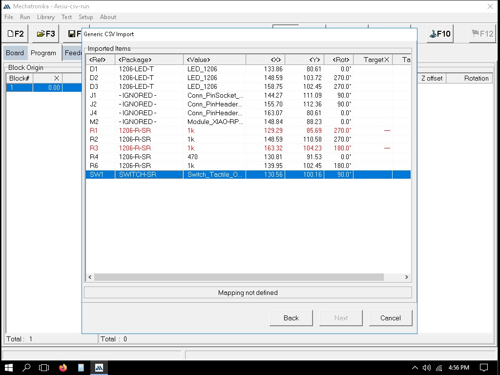
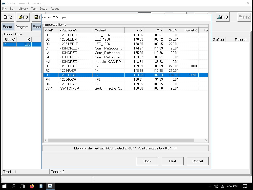
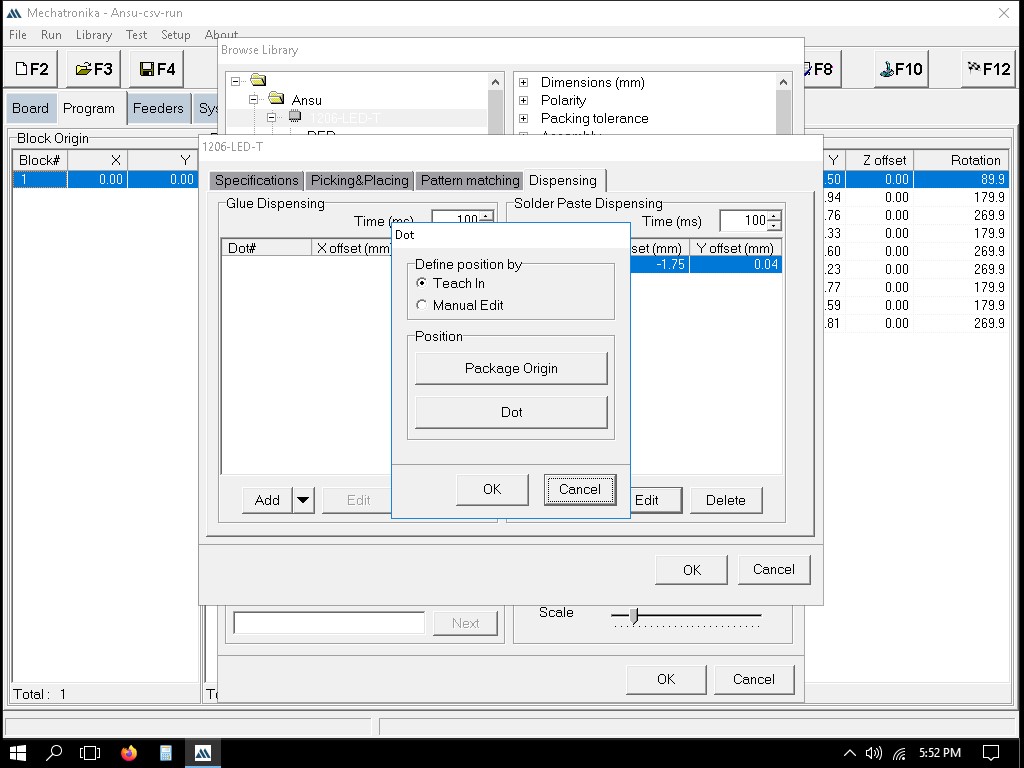
We can define the exact locations where solder paste dots should be placed. This is usually done by clicking on the pads in the PCB layout where paste is needed.
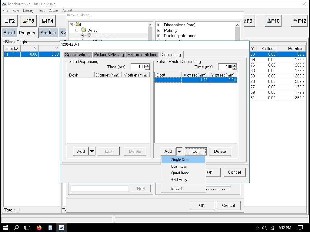
We can manually guide the machine to the points where paste should be applied.
Attaching the soldering paste cartridge
.jpg)
.jpg)
.jpg)
Dispensing
Everything is now set up, and you can dispense the paste: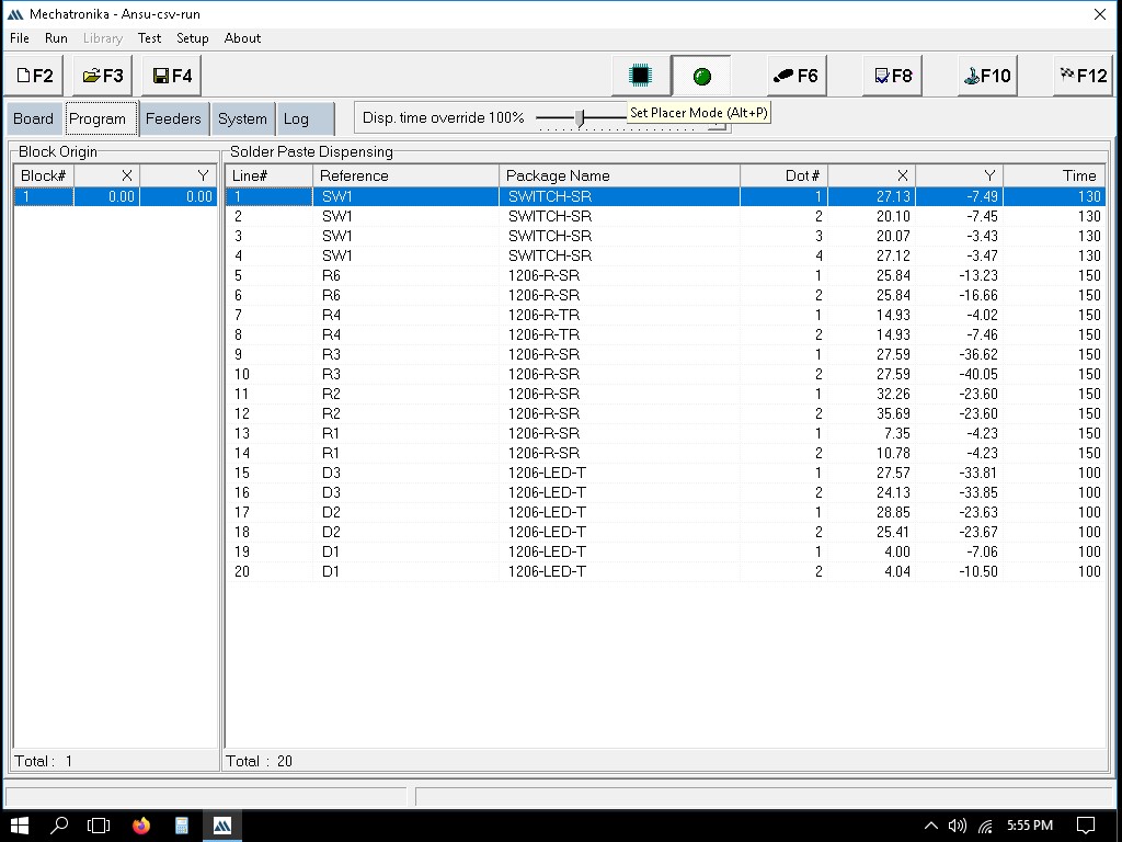
To start placing the components:
Manual Fixing
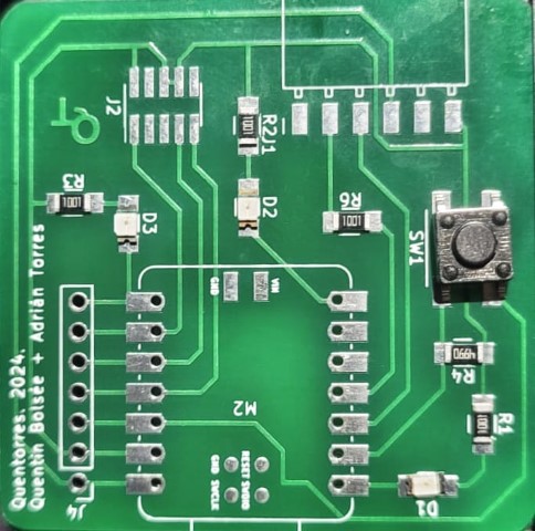
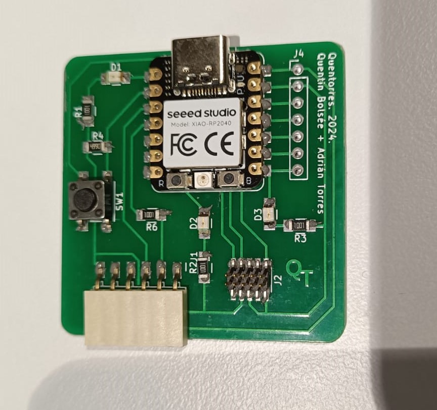
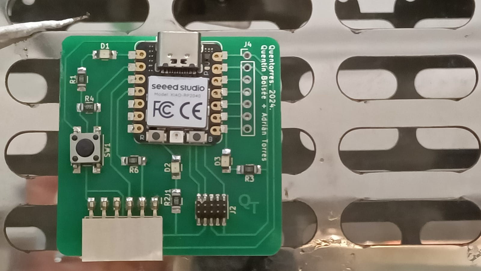
Now, since the Xiao RP2040, the Conn Header SMD 10POS 1.27mm and the Conn Header SMD 6POS 2.54mm couldn't be identified and placed by the machine, it was soldered manually using the paste onto the board.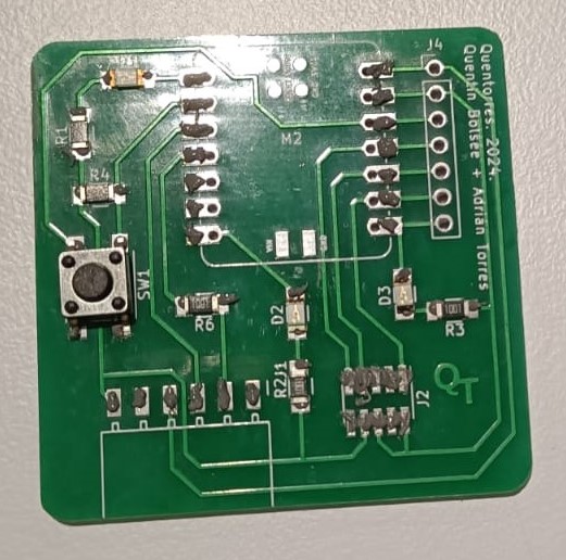
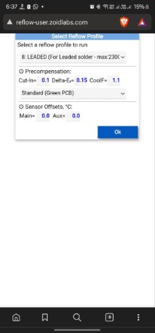
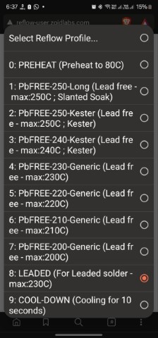
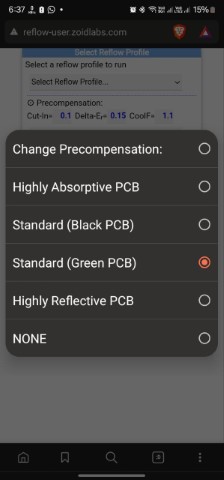
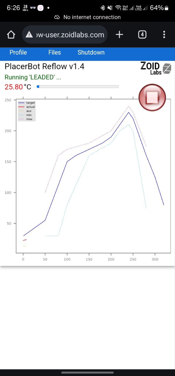
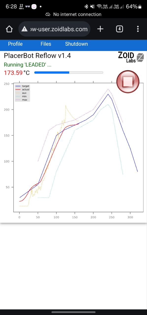
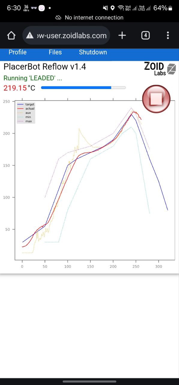
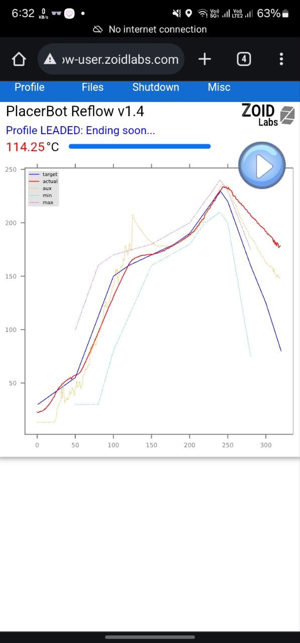
In the oven
.jpg)
.jpg)
Under the microscope
Visual Inspection:.jpg)
.jpg)
.jpg)
.jpg)
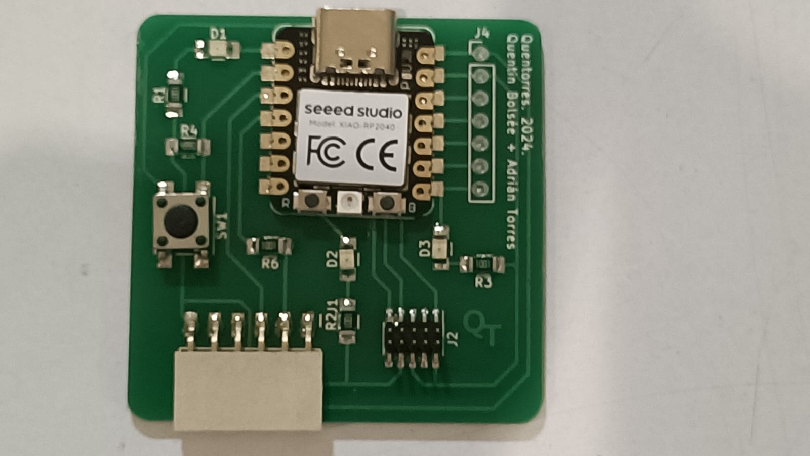
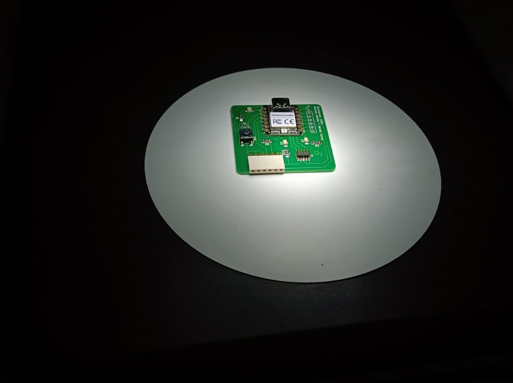
Hero shots