Electronics Design
Assignments
- Group Assignment
- use the test equipment in your lab to observe the operation of a microcontroller circuit board
- Individual Assignment
- use an EDA tool to design a development board to interact and communicate with an embedded microcontroller, produce it, and test it
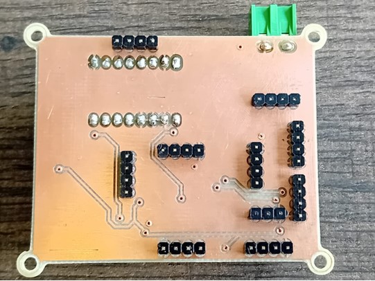
Hero Shots
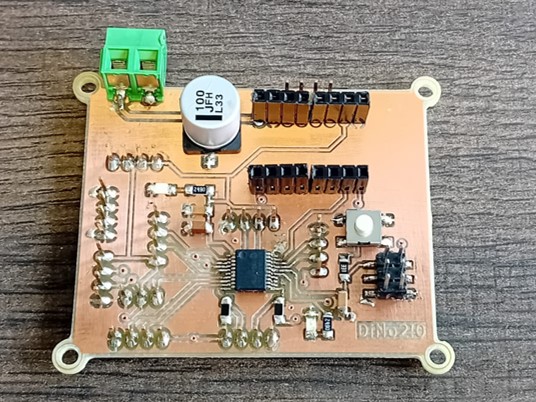
Components and Modules
To start the design, I decided for the modules I need for my final project.
| Module | Information | Link |
|---|---|---|
| Barometric Module | TC-10093132, up to 40 kPa pressure | HERE |
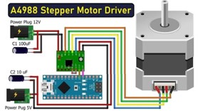
| Stepper Motor | NEMA 17, used in week 06 | HERE |
| Motor Driver | a4988, used in week 06 | HERE |
| Distance Sensor | Ultrasonic sensor HC-SR04, up to 3mm precision | HERE |
| Load Cell | RB-Phi-120, Tension Micro Load Cell (up to 50 kg) | HERE |
| Load Cell Amplifier | HX 711 | HERE |
Barometric Module
- Requirements:
- Can be connected with the hoes of the artificial muscles
- On a breakout board and easily connectable
- Pressure measurement of at least up to 40 kPa
I initially sought a barometric sensor capable of measuring up to 60 kPa, matching the pressure that can be accommodated within the artificial muscle. However, no breakout boards with sensors offering a higher measurement capacity were available. Therefore, I opted to proceed with this choice for the time being. Nevertheless, I aim to explore the possibility of reverse engineering the existing breakout board in the future, with the goal of creating a board compatible with a sensor featuring a higher measurement range.
A barometric high-pressure sensor is designed to measure atmospheric pressure in areas of high pressure. It operates similarly to other barometric pressure sensors but is specifically calibrated to accurately measure pressure levels typically associated with high-pressure systems. When exposed to high atmospheric pressure, the sensor's pressure-sensing element reacts by changing its electrical properties, which are then converted into a measurable electrical signal. This signal undergoes processing to provide a precise reading of the high pressure.
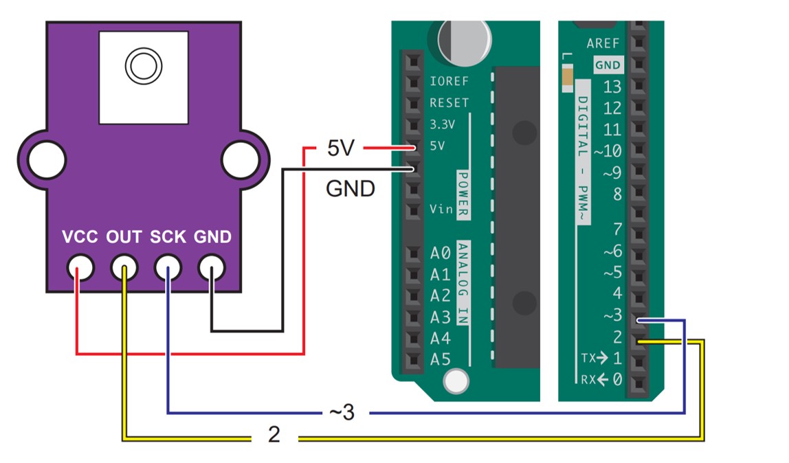
As it can be seen in the picture the module needs a 4 pin connection: GND (Ground), VCC (3.3-5V), OUT (Data), SCK (Clock)
Stepper Motor and Motor Driver
- Requirements:
- strong enough to hold the torque
- On a breakout board and easily connectable
.It's challenging to determine whether the motor can handle the torque generated by the artificial muscle. Personally, I believe that on its own, the motor may not be capable, but with the appropriate gear ratio, it should become sufficient.
NEMA stepper motors are special electric motors that move in precise steps when they receive electrical pulses. They're used in things like 3D printers and CNC machines because they allow for very accurate control of movement.
To make a NEMA stepper motor move, you need a motor driver. This is a device that takes signals from a computer or controller and uses them to power the motor correctly. There are different types of motor drivers, but they all help control the motor's speed and direction.
Motor drivers can do things like make the motor move in smaller steps for smoother motion, limit the amount of current going to the motor to keep it from getting too hot, and protect the motor from damage. They connect to the motor and the control system using wires to make everything work together smoothly.
The connection between the motor driver and the PCB will consists of 10 pins in total. 4 pins for driving and the power source: VCC(5V), Ground (GND), D-Pin (STP), and D-Pin (DIR). 6 Pins for disabling the microstepping, sleep, and reset: 7 Ground (GND) and PWR (5 V).
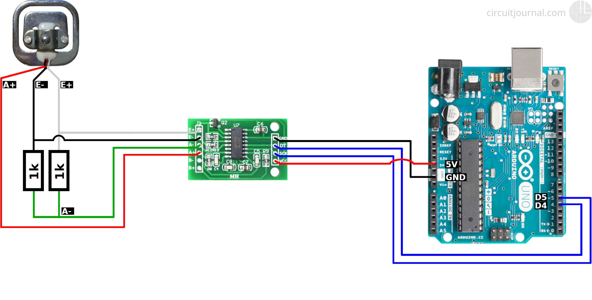
Load Cell and Amplifier
- Requirements:
- Load up to 30 kg
- Tensile measurements
The load cell used for the measurements and to connect to the PCB is the one that meets all the requirements.
A load cell works by using tiny sensors called strain gauges that change their electrical resistance when force is applied to the load cell. These changes in resistance create a small electrical signal. The load cell's circuit, called a Wheatstone bridge, detects this signal and produces a voltage output. An amplifier then boosts this voltage signal for better accuracy. Finally, the amplified signal can be processed further for measurement or display.
The load cell and the amplifier can be connect via 4 pins: Ground (GND), Data (DT), Clock (SCK), and Vcc (5 V)
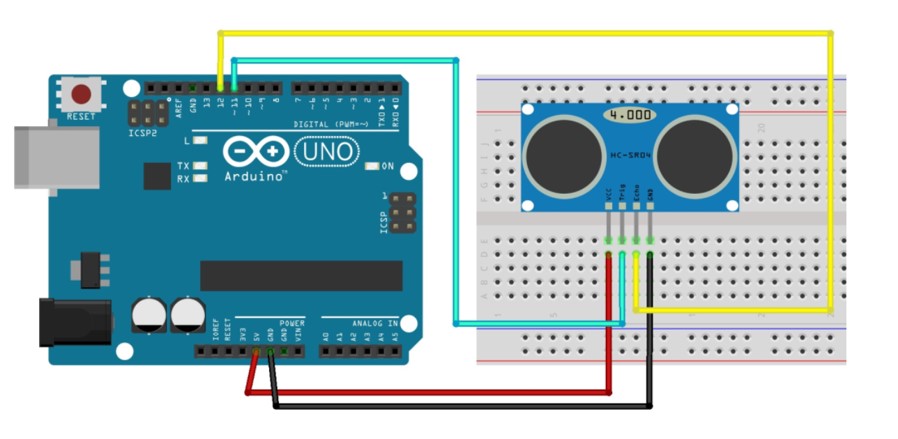
Distance Sensor
- Requirements:
- Measures the distance from 4 cm to 20 cm
- Precision of 1mm
I've opted to utilize the HC-SR04 ultrasonic sensor, despite its precision being set at 3 mm, which ideally falls short of my preference for a higher precision distance sensor. My search for an alternative module with superior precision yielded no results.
For the time being, I've made the decision to proceed with the HC-SR04 sensor I currently possess. However, I remain open to exploring better options in the future should the need arise.
An ultrasonic distance sensor works by sending out high-frequency sound waves from a transmitter. These waves bounce off objects and return to the sensor. By measuring the time it takes for the waves to return, the sensor calculates the distance to the object. This allows it to determine how far away objects are without needing physical contact.
The sensor needs 4 pins: Ground (GND), Echo (D pin), Trig (Analog pin, PWM), and VCC (5 V).
Microcontroller
The big question at hand now revolves around selecting the ideal microcontroller for my project. In my quest, I turned to the microcontroller outlined in the Fabacademy Inventory.
Initially, I leaned towards opting for the one boasting the highest number of pins, memory capacity, and frequency - the ATSAMD21E18A-MU. Seemed like a foolproof choice. However, as I delved into the design process and began mapping out the pin configurations, I found myself inundated with options. Navigating through the multiplexing maze proved to be a daunting task, with the datasheet presenting a rather overwhelming and perplexing array of information.
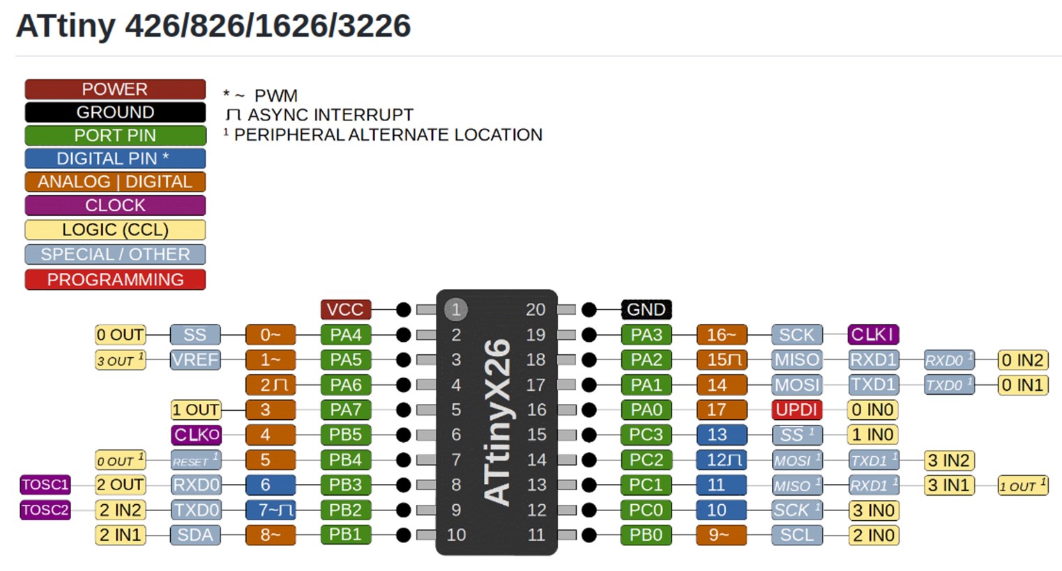
Consequently, I pivoted towards considering the ATTiny3226. It offers an ample number of pins, accompanied by a wealth of readily accessible programming resources and tutorials. Moreover, its straightforward pinout layout renders it much easier to comprehend.
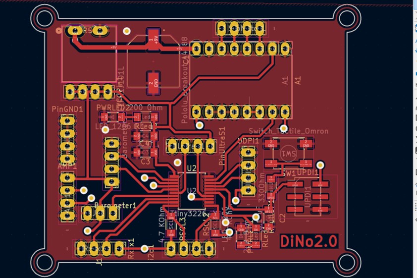
Design
For designing the PCB I used KiCad. As I used the program also in week 04 to design a PCB for the electronic production. For more information for designing a Cpb have a look in the documentation of that week.
Before I started with the design I updated to the latest version of KiCad 8.1.
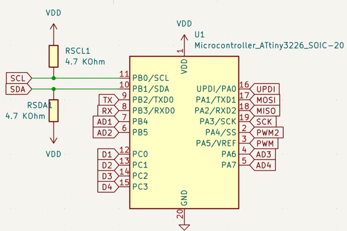
I first inserted the microcontroller and labelled the pins. The data sheet did not specify any information if the pullup resistors for the sda and scl connection is already inside the microcontroller, but the recommendation for the resistors is also not included. Therefore, I planned them to be there, just in case. If there is a problem, because of the high resistance, I can still exchange them.
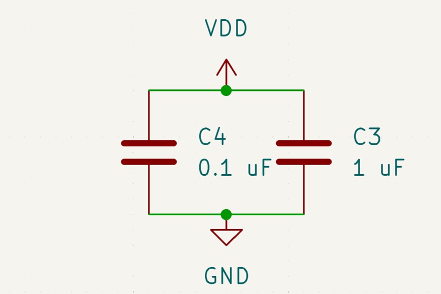
To help with the voltage regulation and prevent voltage overshoot, I inserted two capacitors. In the data sheet three capacitors are recommended, but my instructor said two are enough.
I added all pins that are needed for my components. I noticed, that the Ultrasonic trig pin could need a additional PWM pin, which was not existing on the board :(. Therefore, I used an analog pin with the hope that this still works out.
I then included the communication pins. I changed the updi pin in a way that I can use the recommended programmer for the microcontroller.
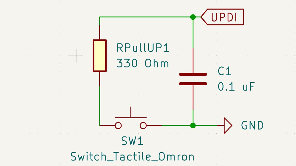
Additionally, a capacitor and a reset button was included to the updi trace, as it is recommended in the data sheet.
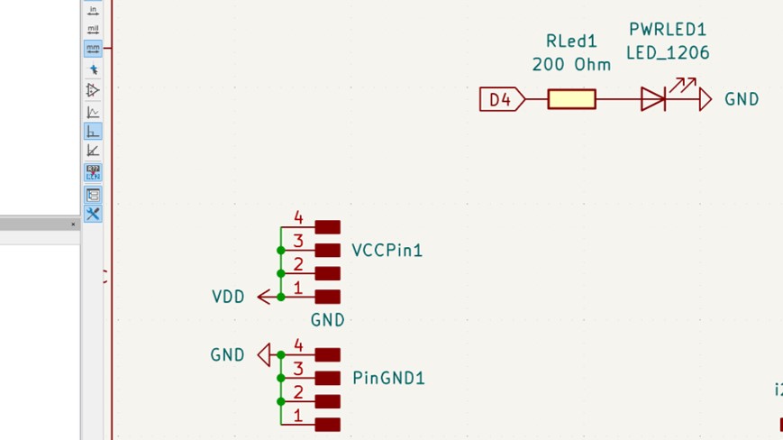
The last piece where additional vcc and GND pins. I included a LED that light up whe the stepper motor would go counter clock wise, and a power LED.
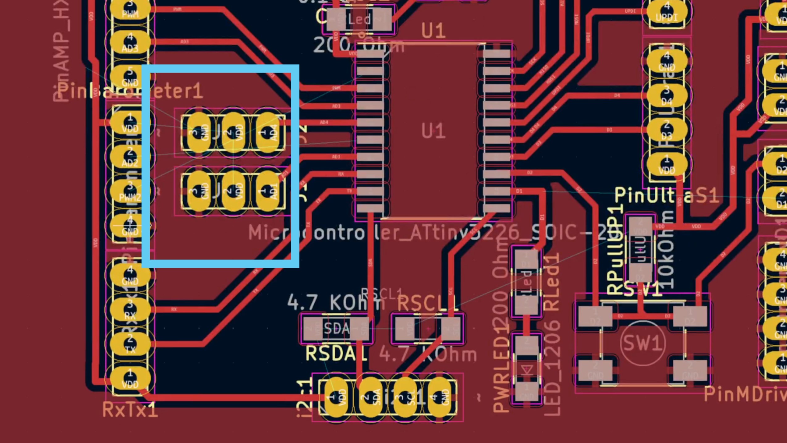
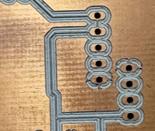
The next step is the PCB Editor. There, all the components where connected. I the first time I trie, I noticed that I could not create the path on one layer without separating some of the pins. So I separated the baraometric, ultrasonic and the 12c pins. Eventough I did that there were still some issues.
The marked area shows the issue I encountered. I tried, to connect these to ground and VDD in several ways, but it just lead to more splitting of pin connection and other issues.
The solution I could think of was a double sided PCB, which can be done in the FabLab in Kamp-Lintfort. Therefore I started to design a back layer in the the PCB editor. With the additional layer I was able to include all the without sepearting them. The layer only included some of the VDD connections and the ground.
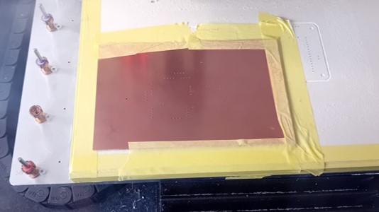
To create the correct output (.grb) for the LPKF (see here) I exported the drill file, the edge cut file, and the two layer milling files. Then I started the machine and its software.
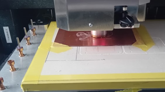
Milling the PCB
To have a clue, how to use the software and the machine look into week 04. I will explain the few changes quickly in this chapter.
For creating a two sided PCB some settings have to be changed and added in the software:
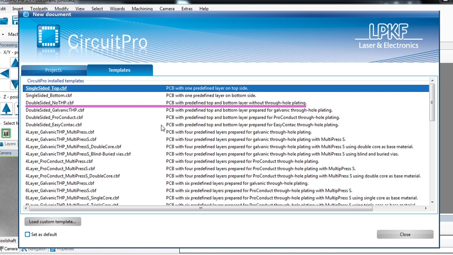
Instead of the "one-sided Top" template choose the "two-sided No THP" template.
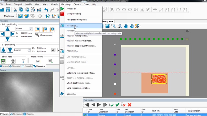
After finishing the isolation process, Go to "Machining" and click on "Placement", have a look where your cooper sheet is and where you want to place the pPCB you designed.
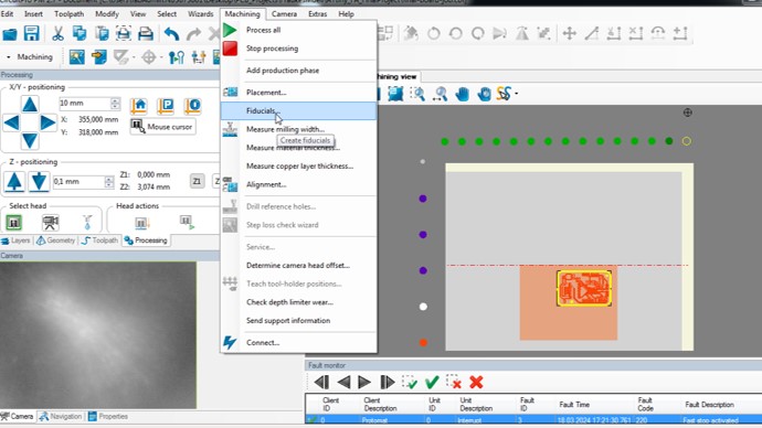
Go to "Machining" and click on "Fiducials".
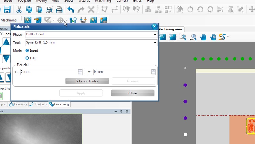
Place two of fiducials OUTSIDE important parts of the PCB. The machine will create two holes to detect the correct placement of the second back layer.
Then you can start the wizard. After finishing the first layer, the machine will prompt you to turn the coppersheet. Manually flip the coppersheet away from your body, positioning it so that it is near the back end of the bed. (shown in the second picture) The machine uses to drilling holes as reference to find the right position of the milling job.
Before flipping, after the first drills.
After flipping.
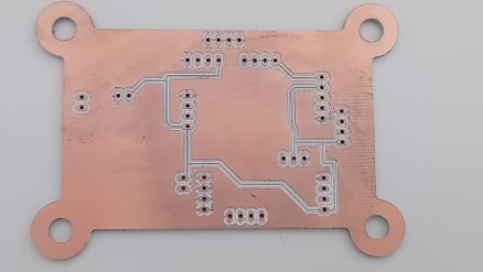
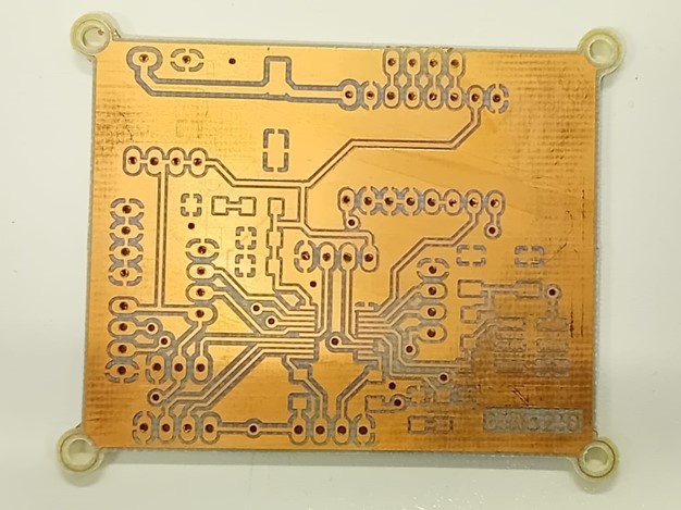
After milling and a little bit of sanding the edges the PCB looked like this:
Due to challenges with auto-focus caused by sunlight (the LPKF mills a test cut and measures the width of the cut to find the zero of the z-axis), the milling of the second bottom layer resulted in excessively deep cuts, leaving very thin traces that may not adequately conduct VDD. Instead of immediately attempting to mill it again, my instructor suggested testing its functionality by connecting the traces in an alternate manner. This interim solution allows us to assess functionality and make any necessary design adjustments before proceeding with another milling attempt.
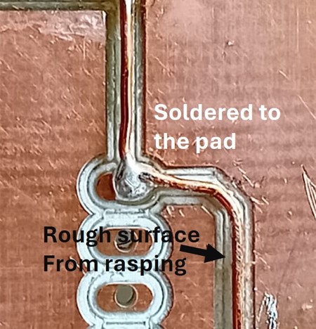
To fix the traces, I used a copper wire and bend it to the paths of the traces missing. I them soldered the wire to the traces. Unfortunately, the alloy of the copper wire or the coating hold back the solder wire from sticking to the wire. Therefore, I had some issues in the beginning, which lead to some ugly solder fails. But these did not interfere with the coninuity or isolation of the traces. To increase the adhesion between the copper wire and the solder wire I used a file to rasp the surface of the cupper wire to make it a little bit rough.
Setback
Despite the failed milling on the back side of the PCB, I was eager to see if my attempt of fixing the traces would work and lead to a conduction of signals. Unfortunately, another setback occured.
For the microcontroller I decided to use the ATtiny3226. Even though, we were working in the local class with the ATtiny 1614 and it would have been easier to use this one, as it was already in stack at the FabLab and most experienced in this lab. The ATtiny 3226 still seemed to be the better option for my purpose, as I needed more pins and as it is mentioned int he FabLab inventory, I decided to use that one. Because this microcontroller was not in stock in the local FabLab our instructor ordered it and it took several days to be delivered.
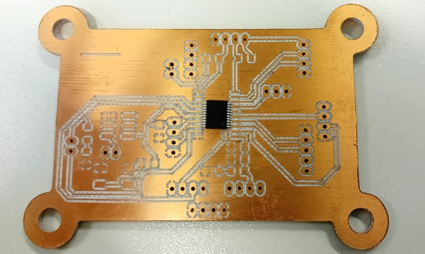
When the microcontroller finally got delivered I noticed, the discrepancy in size of the microncontroller delivered and the footprint milled into the PCB.
The reason for this is, that there are different sizes of the Attiny 3226, which I did not know prior and the footprint int he FabLab library is the one of a ATtiny 3226-SU SOIC-20.
ATtiny 3226-SU SOIC-20 in L.
ATtiny 3226-SU in S.
Re-Design
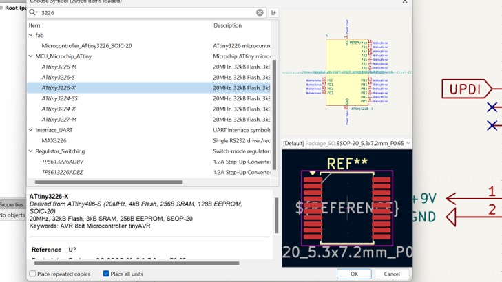
Because of the other size of the ATtiny 3226, I needed to redesign my PCB. Therefore, I needed to the library for the correct microcontroller ATtiny 3226 SOIC-20.
My instructor found a library where all the sizes of the ATtiny 3226 are included (see here).
To my surprise, when including the footprint and symbol to the library of KiCad, I did not need to enter a .sym file. According to my instructor and after measuring the size of the
arrived microcontroller I found out, that the correct symbol symbol and footprint is the one for the ATtiny 3226- SU X. I updates the connections in the schematic file.
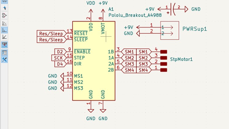
Additionally to the new microcontroller, I included the A4889 (motor driver) pins on the board, so it can be easily connected to the PCB. Therefore, I needed additional pins for the 8-35V power supply for the motor. These needed to be a fixed connection block of 2x1 as well as a capacitor (EEE-FH1J101L) between the connection block and the motor driver.
I then went to the PCB Editor and updated it. To improve the conductivity of traced of the 5V and the 9-35V I decided to create to extra net-classes.
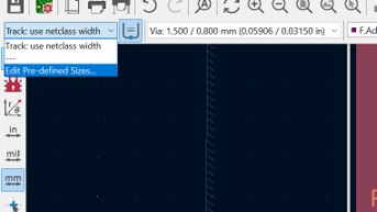
Go to "Track: use net class width" and select "Edit Pre-defined Sizes".
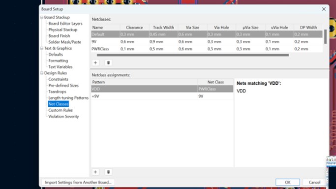
A new window occurs. Click on "Netclasses". Click on the "plus" symbol the netclasses to define the name, clearance, and track width. Then go to "Netclass assignments" and click on the plus to assign a netclass to a track name. After that, click on "ok".
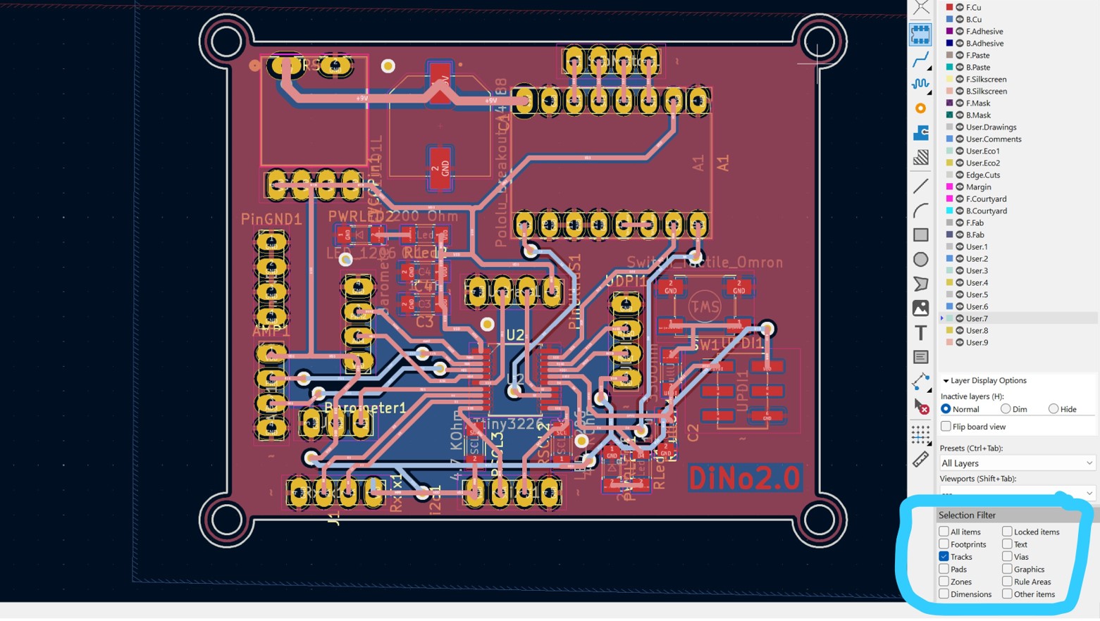
Thereafter select only "tracks" in the bottom left corner and press "strg + A" to select all tracks.
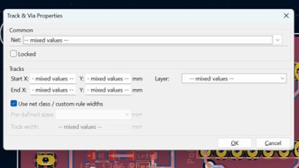
Press "E" to open the properties and enable "Use net class / custom rule widths" then click on ok.
If you press "B" to update the PCB now, the tracks should have the assigned widths and clearances.
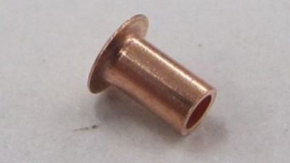
Additionally, I decided to use vias to connect the back and front copper layer rather than using the pin holes, as I would have needed to solder on both sides.
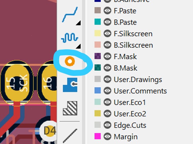
To create vias click on the dot shapes symbol the sidebar on the right side. After correctly positioning your vias, it is necesarry to define the right size for the hole and the diameter for your rivets.
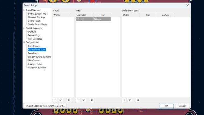
Go to "Track: use net class width" and select "Edit Pre-defined Sizes". Click on "Pre-defined Sizes". Click on the "plus" symbol at the "Vias" to define the diameter and hole. After that, click on "ok".
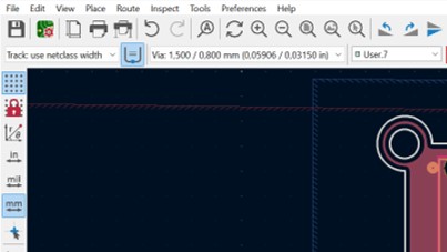
Select the vias size in the upper left corner.
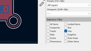
Then got to the bottom right corner and only enable the vias. Then press "Ctrl + A" to select all the vias.
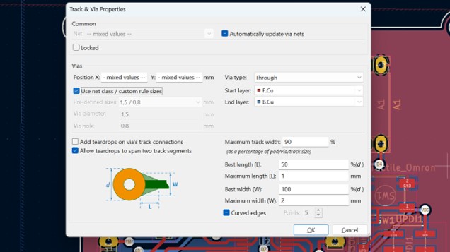
Press "E" to open the "properties" window and enable "Use net class / custom rule widths", then click on ok.
Thereafter, I exported the grb. File for the LPKF and started the milling job on the LPKF.
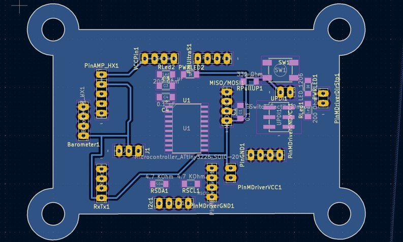
finished design of the front layer
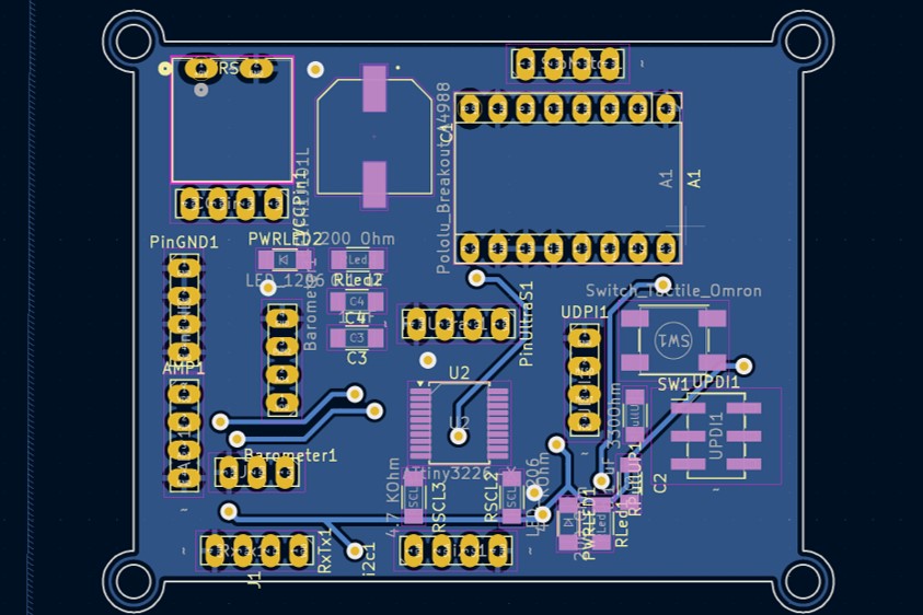
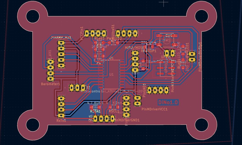
finished design of the back layer
Milling the Re-Design
For the milling process I used the instructions from week 4 and the additional settings needed for a two-sided PCB described in the previous chapter.
Due to ongoing issues with the auto z-leveling process, my instructor decided to closely monitor the leveling procedure. During observation, I identified another potential cause for the failed traces milling in the initial design – a possible bug.
When manually setting the test cut for auto leveling on the LPKF, a warning is generated upon placing the cut on the board. If you opt to redefine the cut placement, the LPKF proceeds without engaging the auto leveling feature.
When this bug occurred, I aborded the process and restarted the cut.
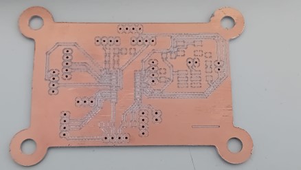
Front Layer
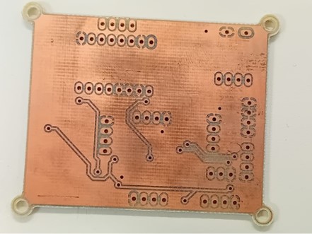
Back Layer
Soldering
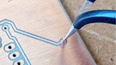
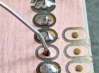
Before beginning the soldering process, I first inserted the rivets. Using a pair of tweezers, I carefully picked up each rivet and inserted it into its corresponding drill hole on the PCB. I gently pressed the rivet into place using the back of the tweezers.
Next, I utilized a press rivet tool to firmly secure the rivet to the PCB. This ensured that the rivet was securely fixed in its position.
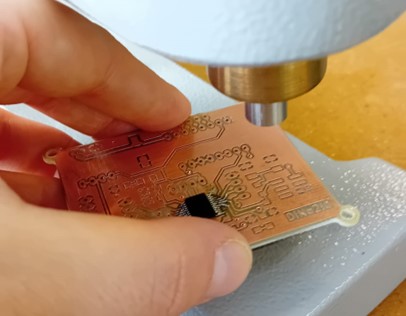
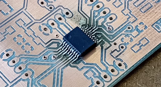
Once the riveting was complete, I proceeded to solder the microcontroller onto the board. As the ATtiny3226 is relatively small, my instructor showed me another method to solder the microcontroller onto the board.
- Apply a small amount of solder to one pad for a corner pin of the microcontroller.
- Position the microcontroller correctly on the board and heat up the pin with the solder beneath it, using the soldering iron until the controller is securely fixed.
- Verify the alignment of the pins to their respective pads under a microscope. If misalignment is observed, reheat the solder and adjust the controller accordingly.
- Begin soldering one side of the controller, ensuring that each pin receives sufficient solder (oversolder).
- Utilize desoldering wire to remove excess solder, leaving only the solder between the pins and the pads on the PCB.
- Test the connectivity of the pins and pads using a multimeter. Additionally, confirm that adjacent pins are not inadvertently connected.
- Repeat the process for the other side of the microcontroller.
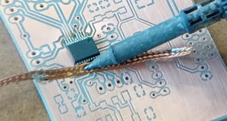
I then soldered the small flat pieces, such as the resistors, the LEDs, the capacitors, and the button.
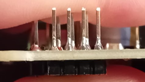
The subsequent step involved soldering the pins onto the PCB. For the male pins, I employed a distinct method. Firstly, I compressed the plastic housing to one end of the pins. Then, from the backside of the PCB, I inserted the pins through the designated pin holes and soldered them onto the front side of the board. This ensured a secure attachment of the pins while maintaining proper alignment with the PCB.
Next, I attempted soldering female pins for the first time. Initially, I followed the method recommended by Frake Waßmuth. I fixed one pin of the female pin header to the board by soldering it in place and carefully readjusted its position as needed to ensure the pins were orthogonal to the PCB. Subsequently, I proceeded to cautiously solder each pin on the front layer. However, despite my efforts, this approach did not yield a satisfactory finish. In light of this, I opted for a different approach to tackle this challenge.
I decided to start soldering from the back of the PCB to ensure a secure connection between the front and back pin pads. To achieve this, I used solder wire with a diameter of 0.5 mm. I inserted the solder wire between the pin and the pin hole, exerting pressure until it couldn't be pushed further inside the hole. Then, I heated up the pin with the soldering iron until the wire melted, effectively soldering the pin to the pad on the back side of the PCB. Even though I didn't directly apply solder on the pad of the front side, I ensured connectivity by employing this method and verified continuity between both pads.
Testing the PCB
For programming the PCB. I first needed to test the concuctivity at first with the multimeter.
I conducted a thorough test to ensure that each pin of the microcontroller was correctly connected to its corresponding pin header and that the ground and VDD were not inadvertently connected. Upon confirming that everything was as intended, I proceeded to connect the PCB to a power supply and ground.
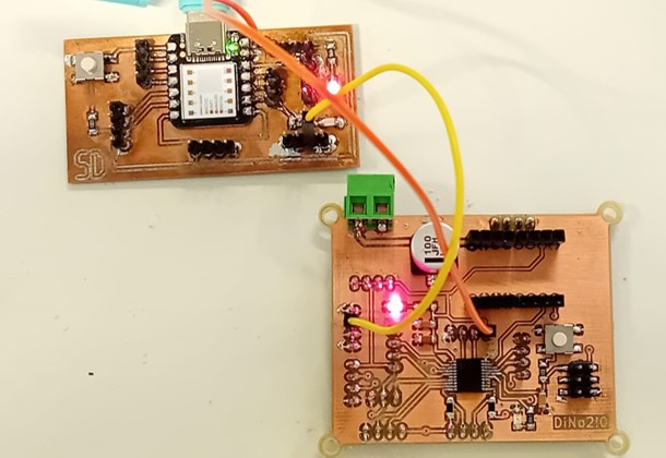
The illumination of the power LED confirmed the successful connection of the VDD pins and Ground pins, respectively. This provided assurance that the connections were sufficient and functioning as intended.
The next step was to test if the microcontroller is programmable witht he UPDI connection. I used the Arduino IDE as a programming environment. As the board manager for the ATtiny 3226 used in this assignment, I installed the Arduino IDE v. 1.8.18 (see here).
After that the correct board manager needed to be installed.
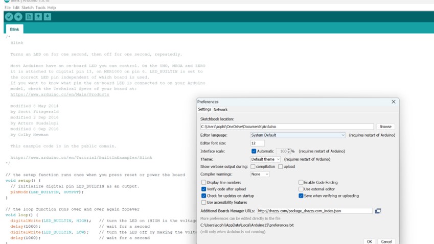
Click on "File" and go to "Preferences". Then paste this link "https://drazzy.com/package_drazzy.com_index.json" to the "Additional Board Manager URL".
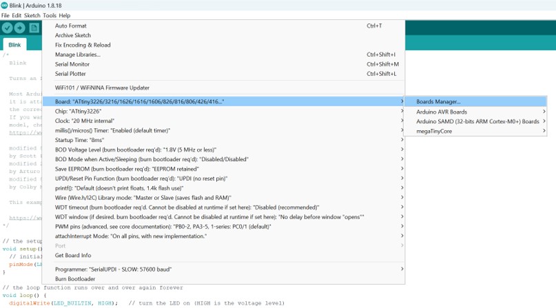
Go to "Tools", then "Board", and click on "Board Manager".
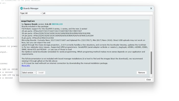
Search the for Attiny in the search bar and install the "magaTinycore" by Spence Konde.
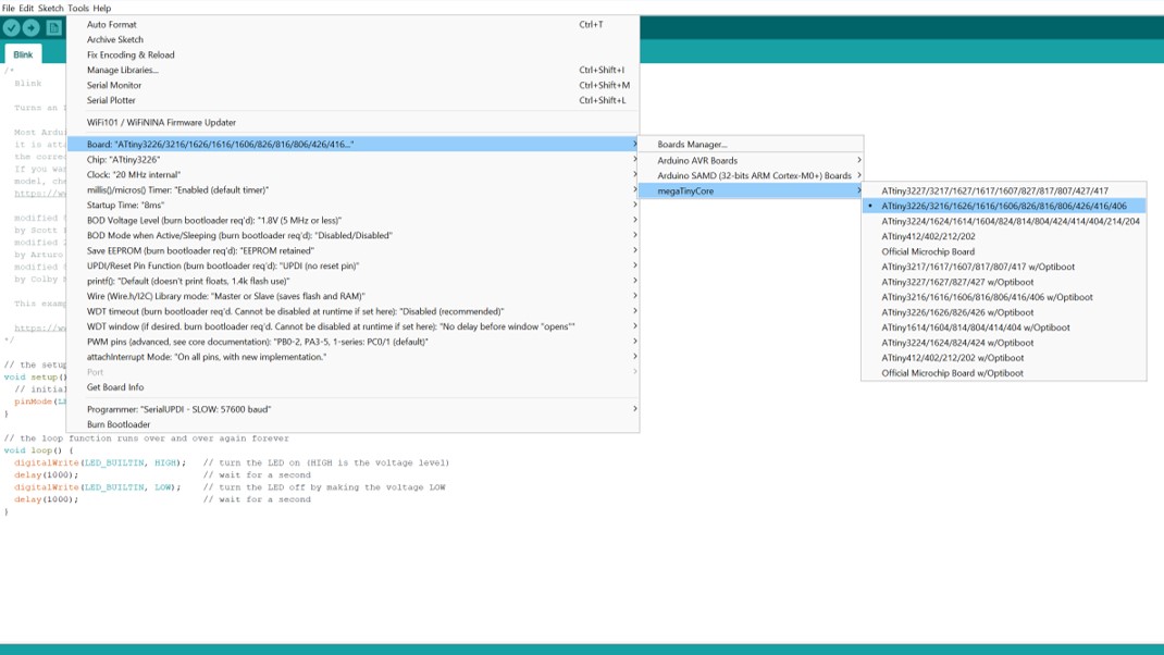
Go to "Tools", then "Board", and select rhe Attiny cor of the Attiny3226
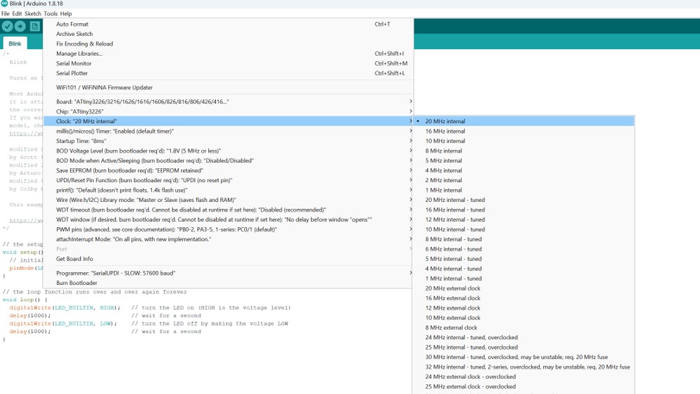
Go to "Tools", then "Clock", and click on "20 MHz internal".
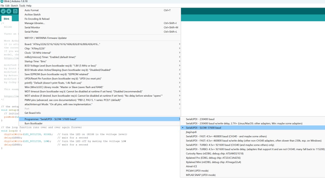
Go to "Tools", then "Programmer", and click on "SerialUPDI -SLOW: 57600 baud".
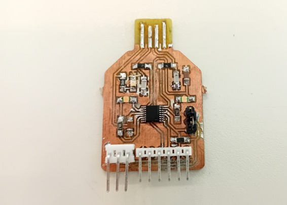
Next, I utilized a programmer board to establish a connection between the computer and the PCB, enabling the programming of the board.
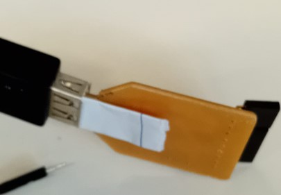
Initially, the connection of the programmer did not function properly, seemingly due to a loose fit in the USB port. To address this issue and ensure a secure connection, I inserted a piece of paper to provide a tighter fit.
Unfortunatetly, the conenction still did not work properly. My instructor suggested to remove the capacitor soldered in a parallel circuit to the UPDI pin, as it is recommended in the data sheet. Interestingly, this solved the issue with the connection of the programmer. Why is it recommended on the data sheet then? (ಠ╭╮ಠ)
After that the connection worked for the first time, allowing to upload a blink sketch to the board. I looked up the right pin for the second LED I included on the board (different depending on the IDE, even though it is "Pin 15", the pin is addressed as "13" in the Arduino IDE).
void setup() {
	// initialize digital pin LED_BUILTIN as an output.
	pinMode(13, OUTPUT);
	}

	// the loop function runs over and over again forever
	void loop() {
	digitalWrite(13, HIGH);   // turn the LED on (HIGH is the voltage level)
	delay(1000);                       // wait for a second
	digitalWrite(13, LOW);    // turn the LED off by making the voltage LOW
	delay(1000);                       // wait for a second
	}